Note : Les descriptions sont présentées dans la langue officielle dans laquelle elles ont été soumises.
CA 02656644 2009-01-02
WO 2008/005993 PCT/US2007/072763
TRANSFORMER AND ASSOCIATED METHOD OF MAKING
USING LIQUID CRYSTAL POLYMER (LCP) MATERIAL
The present invention relates to the field of transformers, and more
particularly, to making a transformer using ceramic, ferrite or liquid crystal
polymer
materials.
Miniature, low cost, small-signal transformers for impedance matching
and conversion of single-ended to differential (BALUNS) are sometimes
prohibitively
large for portable designs using standard wire-wound core technology. Some
advances in low temperature co-fired ceramic ferrite tapes and pastes allow
fabrication alternatives to wire-wound cores. For example, some fabrication
processes for a transformer structure or similar device use metallized
magnetic
substrates or green tape processes, such as disclosed in U.S. Patent Nos.
6,007,758
and 5,802,702. For example, vias can be formed through a ceramic body and
sidewalls coated with a conductive material. An aperture can be formed through
the
ceramic body and intersect the via. The unfired ceramic body can be metallized
such
that a conductive pathway is formed. Also, some devices can be formed from
multiple unfired ferrite layers a single via coating step, permitting green
tape-type
fabrication.
Other processes use traditional low temperature co-fired ceramic
(LTCC) and ferrite tape/ink combinations, such as disclosed in U.S. Patent
Nos.
5,312,674 and 5,532,667. For example, a ferromagnetic material can be provided
in
ink or tape form and sinterable, using a firing profile that is about the same
thermal
shrinkage characteristics as low temperature co-fired ceramic tape.
Other magnetic components can be fabricated as monolithic structures
using multilayer co-fired ceramic tape techniques such as disclosed in U.S.
Patent No.
5,349,743. Multiple layers of a magnetic material and an insulating non-
magnetic
material can form a monolithic structure having magnetic and insulating non-
magnetic regions. Windings can be formed using screen-printed conductors
connected through the multilayer structure by conducting vias.
-1-
CA 02656644 2009-01-02
WO 2008/005993 PCT/US2007/072763
Improvements are still desired to ensure that traditional thick film
printing and commercially available multilayered ceramic (ferrite) tape
processing
can be used with silver and gold thick film conductors without wire winding.
It is
desirable that small designs be implemented for high frequency, small-signal
applications having a low profile. Flexible designs are desirable that allow
the
conductor and core to be integrated. A minimum number of layers is desired
with a
simple pattern to provide a tightly coupled interaction between primary and
secondary
windings.
A transformer and method of making includes first half primary and
secondary windings as metallic circuits that are etched on a metallic cladding
of a first
liquid crystal polymer (LCP) sheet such that secondary windings are positioned
in
spaced relation to the primary windings. A second LCP sheet is applied over
the first
LCP sheet. Second half primary and secondary windings are etched as metallic
circuits on a metallic cladding of the second LCP sheet. Respective first and
second
half primary windings are interconnected to each other and the first and
second half
secondary windings are connected to each other by conductive vias.
The conductive vias can be formed as plated through-holes or punched
holes that are filled with a conductive fill material.
In yet another aspect, the first and second LCP sheets can be fused
together within an autoclave. The first and second LCP sheets can be biaxially
oriented. Ferrite fillers can be provided within at least one of the first and
second
LCP sheets. A ferrite layer can be added between first and second LCP sheets.
In another aspect, the LCP sheets can be between about 25
micrometers to about 3 millimeters thick. The metallic cladding can be formed
as a
copper cladding in one non-limiting example.
Other objects, features and advantages of the present invention will
become apparent from the detailed description of the invention which follows,
when
considered in light of the accompanying drawings in which:
-2-
CA 02656644 2009-01-02
WO 2008/005993 PCT/US2007/072763
FIG. 1 is a plan view of a prior art circuit board showing various
electronic components and three "small" transformers as mini-circuits that are
formed
using standard designs and showing the large profile of such prior art
transformers.
FIG. 2 is an isometric, partial phantom drawing view of a prior art
composite magnetic component structure.
FIG. 3 is another isometric drawing of a prior art composite magnetic
component structure similar to that shown in FIG. 2, but showing a different
orientation of internal components.
FIG. 4 is a plan view of a transformer in accordance with one non-
limiting example of the present invention.
FIGS. 5-10 are plan view drawings showing a sequence of steps used
for manufacturing the transformer shown in FIG. 4.
FIG. 11 is a plan view of another example of a transformer in
accordance with a non-limiting example of the present invention.
FIGS. 12-15 are plan views showing a sequence of steps used for
manufacturing the transformer shown in the example of FIG. 11.
FIG. 16 is a flowchart illustrating an example of the steps used for
manufacturing a transformer using liquid crystal polymer (LCP) sheets.
FIG. 17 is a sectional view of a transformer formed by using LCP
sheets in accordance with the exemplary steps described in the flowchart of
FIG. 16.
Different embodiments will now be described more fully hereinafter
with reference to the accompanying drawings, in which preferred embodiments
are
shown. Many different forms can be set forth and described embodiments should
not
be construed as limited to the embodiments set forth herein. Rather, these
embodiments are provided so that this disclosure will be thorough and
complete, and
will fully convey the scope to those skilled in the art. Like numbers refer to
like
elements throughout.
In accordance with non-limiting examples described throughout this
description, the transformer and method of making as described allows the use
of
traditional thick film printing and commercially available multilayer ceramic
(ferrite)
-3-
CA 02656644 2012-07-04
tape processing that can be co-fired with metallic thick film conductors, for
example,
silver or gold as non-limiting examples. No wire winding is required and small
designs are possible for high frequency, small-signal applications. The
transformer
has a low profile for volume efficient designs that are more flexible because
the
conductor and core are integrated. The transformer design as described can use
simple patterns and a minimum number of layers that provide tightly coupled
interaction between primary and secondary windings. It is also possible to use
liquid
crystal polymer (LCP) sheets to manufacture the transformer in accordance with
non-
limiting examples of the present invention.
The transformer can be adapted for use with radio frequency (RF) and
intermediate frequency (IF) circuits and miniaturized for problematic and
common
components. The transformer can use materials that are commercially available
and
be manufactured using a commercially available process. This transformer
structure,
in accordance with a non- limiting example of the present invention, has a
broad
applicability in the commodity transformer market and in portable wireless
designs.
It can be especially relevant to many S-band receiver designs.
For purposes of description, there follows a brief description of various
prior art designs, followed by non- limiting examples of a transformer and
method of
making same in accordance with a non- limiting example of the present
invention.
FIG. 1 shows a plan view of circuit board 10 having numerous electronic
components
mounted thereon, including integrated circuits (IC's) 12 and numerous other
electronic
components 14. Three "small" transformers as mini-circuits are mounted on the
circuit
board 10. These prior art transformers can be formed using standard wire-wound
core
technology. These types of prior art transformers have a high profile and
large footprint.
In some instances, the prior art transformers extend vertically a greater
distance than
many of the other components 12, 14 that are illustrated and mounted on the
circuit
board 10.
Another prior art monolithic structure uses multilayer co-fired ceramic
tape techniques and examples are shown in FIGS. 2 and 3. The fabrication of
these
magnetic components, such as transformers, uses multiple layers of magnetic
material
-4-
CA 02656644 2009-01-02
WO 2008/005993 PCT/US2007/072763
and insulates the non-magnetic material to form a monolithic structure with
well-
defined magnetic and insulating non-magnetic regions. Windings can be formed
using screen-printed conductors connected through the multilayer structure by
conducting vias.
It should be understood that co-fired multilayer construction has been
found to be increasingly competitive with the traditional thick film
technology in the
fabrication of microelectronic circuit packages. Co-fired multilayer packages
can be
constructed with unfired green (dielectric) ceramic tape for the various
layers.
Compatible conductive compositions can use printed conductor layers
interspersed
between the dielectric layers, and interlayer connecting vias. The conductive
layers
are normally printed on the green tape, and the entire assembly is laminated
and fired
in one operation. It can reduce the physical size of circuitry and improve its
reliability.
The prior art examples shown in FIGS. 2 and 3 are explained in U.S.
Patent No. 5,349,743. Pluralities of the two ceramic green tape materials are
layered
with a desired geometry to form a laminated structure with well-defined
magnetic and
non-magnetic regions. Conducting paths are deposited on selected insulating
non-
magnetic tape layers. These conducting paths are connected by vias formed in
the
layers to create desired multi-turn windings for the magnetic component.
The conducting paths can be constructed of a conductive material that
is amenable to printing or other deposition techniques, and is compatible with
the
firing and sintering process characteristics of ferrite materials. Suitable
conductive
materials include palladium (Pd) or palladium-silver compositions (Pd-Ag)
dispersed
in an organic binder. Other suitable compositions include conductive metallic
oxides
(in a binder), which have the same firing and sintering characteristics as the
ferrite
materials used in constructing the magnetic devices.
The structure formed by the layering technique is laminated under
pressure and co-fired and sintered at a temperature of 1100 to 1400 degrees
Centigrade to form a monolithic magnetic component structure having the
desired
electrical and magnetic properties.
-5-
CA 02656644 2009-01-02
WO 2008/005993 PCT/US2007/072763
To increase electrical resistivity and further reduce the low
permeability of the second tape material, the Ni ferrite powder material is
doped with
Mn to a content equaling 1-10 mol% of the overall material composition.
The component shown in FIG. 2 is constructed as a multiple winding
transformer having a toroidal magnetic core structure. This toroidal core has
four
well-defined sections 31-34, each of which is constructed from a plurality of
high
permeability ceramic green tape layers. Sections 32 and 34 are circumscribed
by
conductive windings 35 and 36, respectively. Taken separately these windings
form
the primary and secondary windings of a transformer. If these windings are
connected
in series, however, the structure functions as a multiple turn inductor.
Windings 35
and 36 can be formed by screen-printing pairs of conductor turns onto a
plurality of
insulating non-magnetic ceramic green tape layers. Each insulating non-
magnetic
layer can have suitable apertures for containing the sections of magnetic
green tape
layered inserts.
The turns printed on each layer are connected to turns of the other
layers with conductive vias 37, i.e., a through hole filled with a conductive
material.
Additional insulating non-magnetic layers are used to contain sections 31 and
33 of
the magnetic tape sections and to form the top and bottom structure of the
component.
Conductive vias 38 are used to connect the ends of the windings 35 and 36 to
connector pads 39 on the top surface of the component. The insulating non-
magnetic
regions of the structure are denoted by 40. Current excitation of the windings
35 and
36 produces a magnetic flux in the closed magnetic path defined by the
sections 31-34
of the toroidal core. The fluxpath in this embodiment is in a vertical plane,
e.g., the
x-z plane shown in FIG.3.
A phantom view of another prior art magnetic component is shown in
FIG. 3. This component, as in the case with the prior example, is also
constructed as a
multiple winding transformer having a toroidal magnetic core structure. A
major
difference from the embodiment of FIG. 2 is that the flux path is horizontal,
i.e., in the
X-Y plane. The toroidal core is defined by a main structure of magnetic
material 41
positioned between top and bottom members 55 and 56, which are insulating non-
-6-
CA 02656644 2012-07-04
magnetic material layers. Member 41 is further punctuated by inserts of
insulating
non-magnetic material inserts 42, 43, and 44, which provide support for
conducting
vias 61, which form part of the windings. The windings 51 and 52 are the
primary
and secondary, respectively, of the transformer. Windings 51 and 52 may be
connected in series to form an inductor. These windings are formed by screen
printing conductors on a layer of member 55 near the top of the structure and
screen
printing conductors on a layer of member 56 near the bottom of the structure
and
interconnecting these printed conductors with the conducting vias 61 to form
the
windings. Connector pads 57 are printed on the top surface of the top layer of
member
58 and are connected by conducting vias 62 to the windings 51 and 52.
Two different transformer structures, in accordance with non-limiting
examples of the present invention, are shown in FIGS. 4 and 11, showing
primary and
secondary windings on a common core. FIG. 4 illustrates a transformer at 100
and
shows a rectangular configured core 102 having an open area 104. The steps
used for
manufacturing the transformer 100 shown in FIG. 4 are shown in FIGS. 5-10.
Respective primary and secondary windings 106, 108 are illustrated.
FIG. 5 is a plan view showing a substantially planar base 110 formed
in this example as a substantially planar ceramic substrate for a fabrication
sequence
as a thick film substrate. A substantially planar configured, first half
primary winding
112 is formed on the ceramic substrate 110. This winding can be typically
formed by
screen-printing a metallic conductor on the base 110, for example, a silver or
gold
screen-printed conductor. The base ceramic material could be an alumina type
ceramic in one non-limiting example. As illustrated, an end 112a of the first
half
primary winding 112 extends beyond the other coil ends, and is operative as
one of
the connection points, i.e., terminals for the completed transformer 100.
Standard
photolithography techniques can be used for printing the metallic conductors.
As shown in FIG. 6, a ferrite paste 114 is applied to the first half
primary winding 112 and over the base, leaving the ends exposed. The ferrite
paste
114 could be an inorganic paste, for example, a ceramic slurry that includes
ferrite-
ceramic particles and a binder as a non-limiting example. It can later be
fired for
-7-
CA 02656644 2009-01-02
WO 2008/005993 PCT/US2007/072763
enhanced density and performance. This could be a low temperature system or a
high
temperature system depending on end-use designs. It is also possible to use
tungsten
or molybdenum. It should be understood that it is not necessary to fire at
this step,
although it is possible to conduct one or multiple firings throughout the
process.
As shown in FIG. 7, the second half primary winding 120 is printed on
the ferrite layer 114 such that the ends of this second half primary winding
overlap the
ferrite layer 114 and contact the exposed ends of the first half primary
winding. One
end 120a is longer and forms a terminal connection. Thus, the winding ends
contact
each other and form a completed transformer primary winding over the ferrite
core
formed by the ferrite paste 114. It is possible to overprint the ferrite such
that no
winding conductors formed from the first half primary winding are exposed.
Vias can
be formed in the pattern and either filled with a conductive paste or plated
to form
conductive vias. This could be possible if the ferrite paste is thick and it
is difficult to
overprint the second half primary winding such that winding ends would connect
winding ends of the first half primary winding. Vias can be formed using a
common
thick film process, as described.
The line spacing can be about 2 to about 4 mils. The thick film process
could be about one-half mil, e.g., about 12 microns, up to a thick film system
norm of
2 to about 4 mils in non-limiting examples. It should be understood that it is
also
possible to use a green tape system and vias.
As shown in FIG. 8, a dielectric layer 130 can be deposited over the
second half primary winding 120 as illustrated. This dielectric layer 130
could be a
glass material and similar structure and forms a cavity corresponding to the
cavity 104
shown in FIG. 4. It is also possible to use a material that burns-out and
leaves a hole,
as long as there is some structure left on which to print. The hole could be
formed
through evaporation in some manufacturing sequences.
As shown in FIG. 8, a first half secondary winding 140 is printed on
the dielectric 130, and includes an end 140a that is operative as a terminal
for the
completed transformer. A second ferrite layer 150 is added as shown in FIG. 9,
and
the second half secondary winding 160 is printed on the ferrite layer 150 such
that its
-8-
CA 02656644 2009-01-02
WO 2008/005993 PCT/US2007/072763
ends connect to the ends of the first half secondary winding 140 as shown in
FIG. 10.
One end 160a is operative as a terminal for the completed transformer. Again,
if the
ferrite layer 150 is thick, the layer could be overprinted on the first half
secondary
winding 160. Conductive vias could be used to attach the first half secondary
winding 140 and second half secondary winding 160. A coating or other layer
could
be applied subsequent to the step shown in FIG. 10 to aid in protecting the
completed
transformer structure.
A second example of a transformer, in accordance with non-limiting
examples of the present invention, is shown in FIG. 11 and has fabrication
sequence
steps shown in FIGS. 12-15. This transformer design could be used for a mini S-
band
receiver operable at about 2.0 to about 4.0 GHz and designed to replace some
commercial over-the-counter parts. The transformer is illustrated at 200 and
includes
a core 202 with a central portion 204 on which the primary and secondary
transformer
windings 206, 208 are wound.
As shown in FIG. 12, a base layer 210 can be formed as a green tape
layer, for example, an LTCC structure, e.g., an unfired ferrite tape in one
non-limiting
example. A first half primary winding 212 is printed together with the first
half
secondary winding 214 and spaced between the "turns" or printed first half
primary
winding conductors. The conductors are spaced from each other such that the
conductive metallic lines forming the first half secondary winding 214 are
spaced
from any conductive metallic lines forming the first half primary winding 212.
Ends
212a, 214a are exposed, forming terminals for the primary and secondary
windings.
A ferrite layer 220 (FIG. 13) forms a "wrap core" and is applied over
the first half primary winding 212 and first half secondary winding 214. This
ferrite
layer 220 has conductor vias 222 formed therein, which could be formed as
plated
through-holes or punched holes filled with a conductive fill.
As illustrated, a second half primary winding 230 and second half
secondary winding 232 are printed on this ferrite "wrap core" 220 such that
the
winding ends connect to the conductive vias 222 and connect ends of the first
half
primary winding 212 and first half secondary winding 214. Longer ends of each
-9-
CA 02656644 2009-01-02
WO 2008/005993 PCT/US2007/072763
winding 230, 232 form terminal ends 230a, 232a, as illustrated. A layer could
be
placed over the second half primary winding 230 and second half secondary
winding
232 to leave only the ends exposed as illustrated in FIG. 5. This layer could
be a
ferrite layer 250.
It should be understood that any formed cavity is advantageous
because the flux typically stays in the path of least reluctance. If some
cavities are
placed along edges lengthwise next to vias on the outside, it could improve
the
efficiency in some examples.
FIG. 16 shows a flowchart and illustrates a sequence of steps used for
making a transformer structure similar to that shown in FIG. 11, using a
liquid crystal
polymer (LCP). The steps used for forming the transformer could be similar to
those
signs shown in FIGS. 12-15, but with a series of etching steps used instead.
Typically, the liquid crystal polymer could be supplied in sheet form, in one
non-
limiting example, as a biaxially oriented film. It could include an orthogonal
crystal
structure as a biaxially oriented film. Ferrite fillers could be used to
increase
permeability and magnetic properties. The LCP sheets are preferably supplied
as a
laminate that includes a metallic cladding, for example, a copper cladding,
which is
etched to form a partial transformer structure similar to that shown in FIG.
12 with
first half primary and secondary windings, followed by adding another LCP
sheet and
etching to form the second half primary and secondary windings.
As shown in the flowchart of FIG. 16, a first LCP layer can be etched
back (block 300) to form the first half primary and secondary windings. A
ferrite
layer is applied (block 302) in one non-limiting example, and a second LCP
layer
applied and etched (block 304) to form the second half primary and secondary
windings. The vias can be formed (block 306) and a cover layer overlaid (block
308).
The LCP sheets can be fused together such as in autoclave.
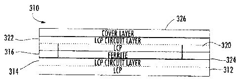
FIG. 17 is a sectional view of the different layers that can be used for
forming the transformer using LCP's. The transformer structure 310 includes a
first
LCP layer 312 that includes an etched back LCP circuit layer 314 forming the
first
half primary and secondary windings. A ferrite layer 316 is added and followed
by a
-10-
CA 02656644 2009-01-02
WO 2008/005993 PCT/US2007/072763
second LCP layer 320 that includes an etched back LCP circuit layer 322 for
the
second half primary and secondary windings. Vias 324 connect between the LCP
circuit layers 314, 322 interconnecting primary windings to each other and
secondary
windings to each other. A cover layer 326 can be added over the second LCP
layer
320. This layer could also have an LCP circuit layer adjacent the ferrite in
some
instances depending on the processing sequences used.
LCP has a unique property and can fuse to itself under pressure. An
autoclave can be used to apply heat and pressure to allow the LCP sheets to
fuse to
themselves. A traditional prepeg process with plated through holes could also
be
used. Thus, it is possible to start with a sheet of LCP material that is
loaded with
ferrite for magnetic transformer properties and copper cladding, which is
etched back.
The first half primary and first half secondary windings can be formed and
another
LCP sheet applied, which is etched back to form the second half primary and
second
half secondary windings. When fully assembled, the vias can be drilled and
plated or
filled with conductive paste.
The liquid crystal polymer is typically formed as a thermoplastic
polymer material and has rigid and flexible monomers that link to each other.
The
segments align to each other in the direction of shear flow. Even when the LCP
is
cooled below a melting temperature, this direction and structure of
orientation
continues. This is different from most thermoplastic polymers where molecules
are
randomly oriented in a solid state.
As a result, LCP has advantageous electrical, thermal, mechanical and
chemical properties. It can be used for high-density printed circuit board
(PCB)
fabrication and semiconductor packaging. It can have a dielectric constant of
about 3
in the range of about 0.5 to about 40 GHz and a low loss factor of about 0.004
and
low moisture absorption and low moisture permeability.
LCP can be supplied as a thin film material ranging from about 25
micrometers to about 3 millimeters. One or both sides can include a copper
cladding
that is about 18 micrometers thick in some non-limiting examples, and could
range
even more. This copper cladding (layer) could be laminated in a vacuum press
at
-11-
CA 02656644 2009-01-02
WO 2008/005993 PCT/US2007/072763
around the melting point of LCP. Micromachining techniques could be used to
allow
MEMS applications. This could include photolithography, metallization, etching
and
electroplating. It is possible that some LCP material can be bonded to MEMS-
related
materials using a thermal bonding process and slight pressure at about the
melting
point or just below the melting point. Complex multilayer, three-dimensional
structures could be formed.
-12-