Note : Les descriptions sont présentées dans la langue officielle dans laquelle elles ont été soumises.
CA 02656659 2009-02-27
1
TRANSMITTER OF A SYSTEM FOR DETECTING A BURIED CONDUCTOR
Field of the invention
The present invention relats to a transmitter of a system for detecting a
buried conductor.
Background of the invention
Before commencing excavation or other work where electrical cables, fibre
optic cables or
other utilities ducts or pipes are buried, it is important to determine the
location of such
buried cables or pipes to ensure that they are not damaged during the work.
Once a buried
utility is located the depth of the utility can be calculated to determine a
safe excavation
depth.
Current carrying conductors emit electromagnetic radiation which can be
detected by an
electrical antenna. If fibre optic cables or non-metallic utilities ducts or
pipes are fitted with
a small electrical tracer line, an alternating electrical current can be
induced in the tracer line
which in turn radiates electromagnetic radiation. It is known to use detectors
to detect the
electromagnetic field emitted by conductors carrying alternating current.
One type of such detector works in one of two modes, namely 'active' or
'passive' modes.
Each mode has its own frequency band or bands of detection.
In passive mode, the detector detects ambient magnetic fields, for example
those produced
by a conductor carrying an AC mains power supply at 50/60 Hz and very low
frequency
(VLF) signais originating from VLF long wave transmitters.
In active mode a signal generator/transmitter is used to produce an
alternating test signal in
the conductor in accordance with one of three mechanisms. If the transmitter
can be directly
CA 02656659 2009-02-27
2
connected to the conductor then an alternating test signal of known frequency
waveform and
modulation is applied directly to the conductor.
If the conductor is accessible but direct connection is not feasible, for
example where the
conductor is carrying live mains power, a clamp can be used to apply the
transmitter test
signal to the conductor. The clamp is typically comprised of a split toroidal
magnetic core
which curies a primary winding magnetising the core with the alternating
transmitter signal.
An alternating signal flowing in the winding produces an electromagnetic
signal in the
conductor similar in operation to a transformer.
Where access to the conductor is not possible, the signal transmitter produces
an alternating
electromagnetic field by use of a strong induction loop. If the transmitter is
placed near to
the buried conductor then the electromagnetic field induces a current in a
nearby buried
conductor.
In ail three mechanisms of stimulating a test signal in the buried conductor
in the active
mode, the buried conductor radiates the signal produced by the signal
transmitter and the
radiated signal can be detected by a detector.
A number of factors must be considered when using the active mode. As the
transmitter is
conventionally powered by on-board batteries it is important to efficiently
generate the test
signal whilst conserving the power expended by the transmitter as much as
possible so as to
prolong the battery life of the transmitter. Therefore the power of a signal
output from the
transmitter should be minimised to reduce battery consumption. In addition, a
high power
signal can couple to unwanted lines and spread over the lines, making it
difficult to detect
the target buried conductor.
The transmitter can be configured to transmit an alternating test signal at a
number of
frequencies and waveform types. The choice of frequency depends on a number of
factors,
1
CA 02656659 2009-02-27
,
3
for example the ease of inducing the test signal into the buried conductor and
interference
from ambient signals.
Regarding the choice of frequency of the alternating test signal, a high
frequency signal is
typically used for a high resistance line or a small insulated telecoms line,
although that
signal decreases more rapidly with distance along the conductor than for a
lower frequency.
A medium frequency signal is typically used for mains power supply cables and
continuous
metal pipes and a low frequency signal is used for long distance tracing where
a defined
termination is used (earth).
A problem with conventional signal transmitters is that the transmitter
performs poorly in
response to a change in the load, which can lead to damage to the transmitter.
Although
conventional signal transmitters comprise a basic feedback loop to stabilise
the signal output
from the transmitter, the control law used does not allow the transmitter to
react quickly to
changes in the load. For example, sudden disconnection of the load may not be
expediently
detected by the transmitter, resulting in driving the amplifiers too hard and
potentially
damaging the transmitter. In addition, the feedback loop can detect and
process ambient
signals and inefficiently drive amplifiers in the transmitter based on the
ambient signais.
In this application we describe an improved transmitter of a system for
detecting a buried
conductor which overcomes some of the disadvantages of conventional systems.
Summary of the invention
According to a first aspect of the invention there is provided a transmitter
comprising:
means for generating a drive waveform signal; power supply means; amplifier
means
connected to the power supply and the waveform generator for producing an
output drive
signal based on the drive waveform signal; output means for acting on the
output drive
signal to generate an output signal having a current and a voltage; and
feedback means for
i
CA 02656659 2009-02-27
4
controlling the amplifier means on the basis of the output signal wherein the
feedback
means provides in-phase and quadrature components of the current and voltage
of the
output signal.
The feedback voltage and current of the output signal may be filtered through
a narrow band
filter. The narrowband filter may have a bandwidth of less than 100 Hz,
preferably less than
75 Hz or preferably less than 40 Hz.
The narrowband filter may be a sine filter. The sine filter may be implemented
with a finite
impulse response filter.
The feedback voltage and current may be sampled above the Nyquist frequency
with respect
to the transmitter output signal.
The amplifier means may comprise an H-bridge D-class amplifier and a bridge
tied linear
amplifier. The H-bridge D-class amplifier may operate in a range of the output
signal of DC
to 40 KHz.
The H-bridge D-class amplifier may be modulated using a delta-sigma modulation
scheme
in the range of the output signal of DC to 8 KHz and the H-bridge D-class
amplifier may be
modulated using a pulse width modulation scheme in the range of the output
signal of 8
KHz to 40 KHz.
The bridge tied linear amplifier may be driven by the drive waveform signal in
a range of
the output signal above 40 KHz.
The bridge tied linear amplifier may be driven by a variable power supply.
CA 02656659 2009-02-27
The drive waveform signal may be generated by a proportional-integral-
derivative
controller.
According to a second aspect of the invention there is provided a system for
detecting a
buried conductor comprising: a transmitter as described above and a receiver
for detecting a
signal induced in said buried conductor by the output signal of the
transmitter.
According to a third aspect of the invention there is provided a method of
generating a
transmitter output signal comprising: generating a drive waveform signal;
amplifying the
drive waveform signal to produce an output drive signal; generating an output
signal based
on the output drive signal, the output signal having a current and a voltage;
and feeding
back in-phase and quadrature components of the current and voltage of the
output signal for
controlling the amplification.
The feedback voltage and current of the output signal may be filtered through
a narrow band
filter. The narrowband filter may have a bandwidth of less than 100 Hz,
preferably less than
75 Hz and preferably less than 40 Hz.
The narrowband filter may be a sinc filter. The sinc filter may be implemented
with a finite
impulse response filter.
The feedback voltage and current may be sampled above the Nyquist frequency
with respect
to the transmitter output signal.
The amplification may be performed by an H-bridge D-class amplifier and a
bridge tied
linear amplifier. The H-bridge D-class amplifier may operate in a range of the
output signal
of DC to 40 KHz.
The H-bridge D-class amplifier may be modulated using a delta-sigma modulation
scheme
CA 02656659 2009-02-27
6
in the range of the output signal of DC to 8 KHz and the Fl-bridge D-class
amplifier may be
modulated using a pulse width modulation scheme in the range of the output
signal of 8
KHz to 40 KHz.
The bridge tied linear amplifier may be driven by the drive waveform signal in
a range of
the output signal above 40 KHz.
The bridge tied linear amplifier may be driven by a variable power supply.
The drive waveform signal may be generated by a proportional-integral-
derivative
controller.
According to a fourth aspect of the invention there is provided a carrier
medium carrying
computer readable code for controlling a microprocessor to carry out the
method described
above.
According to a fifth aspect of the invention there is provided a method of
detecting a buried
conductor comprising: generating a transmitter output signal as described
above to induce a
test signal in said buried conductor, the test signal generating an
electromagnetic field; and
detecting the generated electromagnetic field.
According to a further aspect of the invention there is provided a transmitter
comprising: a
waveform generator for generating a drive waveform signal; a power supply; an
amplifier
stage connected to the power supply and the waveform generator for producing
an output
drive signal based on the drive waveform signal; an output circuit for acting
on the output
drive signal to generate an output signal having a current and a voltage; and
a feedback
connection for controlling the amplifier stage on the basis of the output
signal wherein the
feedback connection provides in-phase and quadrature components of the current
and
voltage of the output signal.
CA 02656659 2009-02-27
7
Brief description of the drawirws
Figure 1 is a schematic representation of a system for detecting a buried
conductor
according to an embodiment of the invention;
Figure 2 is a block diagram of the transmitter of the system of Figure 1;
Figure 3 is a block diagram of signal processor and output modules of the
transmitter of
Figure 2; and
Figure 4 is a block diagram of the control law controlling the transmitter of
Figure 2.
Description of preferred embodiments
Figure 1 is a schematic representation of a system 1 for detecting a buried
conductor
according to an embodiment of the invention, comprising a portable transmitter
3 and a
portable receiver 5. The transmitter 3 is placed in proximity to a buried
conductor 7 to
produce an alternating current test signal in the buried conductor 7.
An aerial in the transmitter 3 is fed with an AC voltage to produce an
electromagnetic field
9 which links around the buried conductor 7, thereby inducing the alternating
current test
signal in the buried conductor 7. The alternating current test signal is
radiated as an
electromagnetic field 11 by the buried conductor 7 and this electromagnetic
field can be
detected by the receiver 5. In other embodiments the transmitter may provide a
test signal in
the conductor by direct connection to the conductor or by clamping around the
conductor, as
described above.
Figure 2 is a block diagram of the transmitter 3 of the system 1 of Figure 1.
The output
signal of the transmitter 3 is radiated by an output module 13 and coupled
into the buried
CA 02656659 2009-02-27
8
conductor 7 to produce the alternating test signal in the buried conductor 7.
The output
module 13 may also flood an area with an output signal which energises all
conductor lines
in the area.
The operation of the transmitter 3 is determined by an operator either via a
user interface
module 15 or by the commands received at a communications module 17 of the
transmitter
3. The predetermined characteristics of the output signal of the transmitter 3
comprise the
signal's power, frequency and modulation scheme. The power of the signal
output from the
transmitter 3 is primarily controlled by varying the signal's current. Once
the desired
characteristics of the output signal are determined, a signal processor module
19 drives the
output module 13 and monitors the signal output from the output module 13 to
ensure that
the signal output from the output module 13 conforms to the predetermined
characteristics.
The user interface module 15 conveys information to the operator of the
transmitter 3 and
may comprise one or more of a display for displaying information to the
operator of the
device, input devices such as a keypad or a touch sensitive screen and an
audible output
device such as a speaker or beeper. The communications module 17 may send and
receive
commands to/from a communications module of the receiver 5 and/or enable the
transmitter
3 to be connected to a personal computer (PC) or a personal digital assistant
(PDA) (not
shown). The transmitter 3 further comprises a memory module 23 and a power
supply unit
(PSU) 25, acting as a power supply means, comprising power management
circuitry and a
power source such as batteries. The overall control of the various components
of the
transmitter 3 is managed by a controller 21. The components of the portable
detector 3 are
housed in a housing (not shown).
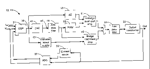
Figure 3 is a block diagram of the output module 13 and the signal processor
module 19 of
the transmitter 3 of Figure 2. The predetermined characteristics of the signal
to be output
from the transmitter 3, which are input by an operator of the transmitter 3,
are passed to a
digital signal processor (DSP) 31 of the signal processor module 19 as a
current demand
CA 02656659 2012-07-19
9
signal, ld.d= The digital signal processor 31 also receives signais
representing the output
current bout and output voltage V. of the transmitter 3. These representative
signals are
generated by monitoring the signal output from an output transformer 33 of the
transmitter 3
to give an analogue output voltage signal; additionally converting the output
voltage using a
current sense stage 35 to give an analogue output current signal; and
digitising the analogue
output voltage signal and the analogue output current signal to give digitised
versions of
these signals which are passed to the DSP 31.
The analogue output voltage signal and analogue output current signal are
digitised in an
analogue-to-digital converter (ADC) 37 at a sampling rate of 500 KHz, this
being above the
Nyquist sampling frequency with respect to the transmitter output signal, the
transmitter 3
operating, in general, at a maximum signal frequency of 200 KHz.
The DSP 31 processes the current demand and digitised output signais and,
acting as a
means for generating a drive waveform signal, generates a drive waveform
signal 39 which
is passed to a digital-to-analogue converter (DAC) 41. The drive waveform may
be a sine
wave, a current direction waveform comprising two signal components of
different
frequency for detecting coupling of the test signal onto a nearby conductor as
described in
WO 90/09601 in the name of Radiodetection Limited, a fault finding waveform
such as the
waveform described in GB 2211621 and EP 0457809 in the name of Radiodetection
Limited, or other waveform to be detected by the receiver 5. The drive
waveform signal 39
is also passed to a variable power supply module 43 which controls the power
supply to a
bridge tied linear amplifier 45, as explained below.
The analogue drive waveform signal 47 output from the DAC 41 is filtered with
an antialias
filter 49, in this case a 5th order Chebychev filter, to remove high frequency
artefacts
resulting from the digital to analogue conversion. This cleaning up of the
output waveform
ensures that energy is not wasted in the power amplifiers.
CA 02656659 2012-07-19
The output module 13 of the transmitter 3 comprises amplifier means and
operates in one of
three output schemes, depending on the frequency of the output signal.
Below around 40 KHz a D-class amplifier is used. The D-class amplifier is
comprised of an
H-bridge of MOSFETs 51 modulated as push-pull switches. In the sub-range of DC
to
around 8 KHz the signal input to the H-bridge amplifier 51 is modulated using
a Delta-
Sigrna (A-s) modulation scheme 53 which is particularly efficient for
generating low
frequencies into low impedance loads. Delta-Sigma modulation is performed by
the DSP
31, the output of which drives the H-bridge directly. Further details of the
Delta-Sigma
10 modulation scheme are provided in GB 2363010 in the name of
Radiodetection Limited.
Above 8 KHz the switching losses in the MOSFETs become dominant so in the
subrange of
8 KHz to 40 KHz the H-bridge amplifier is modulated using a pulse width
modulation
(PWM) scheme 55. The drive waveform signal output from the anti-alias filter
49 is
converted to a sequence of pulses whose average value is directly proportional
to the
amplitude of the signal at that time. The PWM frequency in this case is chosen
as 262 KHz
and is phase locked to the DSP sampling which is a key parameter in overcoming
unwanted
frequency artefacts in the output.
Above 40 KHz the H-Bridge MOSFETs 51 suffer increasingly dominant switching
losses
due to the gate capacitance. Therefore in the frequency range 40 KHz to 200
KHz and above
a bridge tied linear amplifier 45 is used so that a full rail-to-rail voltage
swing is available.
The linear amplifier is fed with the signal directly output from the anti-
alias filter 49. In
addition, the bridge tied linear amplifier 57 is subject to a variable power
rail by means of
the variable power supply module 43 so that intrinsic losses of voltage
regulation can be
minimised for loads and demand where voltage swing across the fully available
rail-to-rail
voltage is not required.
CA 02656659 2009-02-27
11
The outputs of the H-bridge push-pull amplifier 51 and the bridge tied linear
amplifier 45
are fed into a low pass filter 59 to remove unwanted switching artefacts and
the filtered
signal is fed into an output transformer 33. The output transformer 33 is used
to generate an
alternating current test signal in the buried conductor 7 by direct
connection, toroidal
clamping or induction using standard apparatus and techniques as is well known
in the art.
The transmitter provides a maximum load line power of lOW for output signals
up to 40
KHz and a maximum load line power of 1W for output signals above 40 KHz (for
compliance with Electromagnetic Compatibility (EMC) regulations). The 10W load
line is
designed around the standard assumption of a 300 n load which is a typical
impedance for
wet clay conditions. In addition a power efficient amplifier gives the battery
powered
transmitter a good operating life.
The transmitter 3 acts as a programmable current source in a frequency range
from DC to
200 KHz. The transmitter 3 is capable of providing a very stable output, with
no modulation
artefacts visible above ¨80dB. In addition the transmitter 5 is capable of
driving loads of
all conceivable impedance. In particular the transmitter is capable of driving
loads with a
low impedance of only a few ohms, i.e., almost a dead-short, such as an
earthed gas pipe;
very high impedance loads such as insulated cables and dry-soil having an
impedance of 1M
ohm and a 100 nf capacitance; and inductive loads through a clamp.
Figure 4 shows a block diagram of the control law used for controlling the
transmitter 3
which is implemented in the DSP 31 of Figure 3. The DSP 31 receives digitised
inputs 'out
and Vout from the ADC 37 at a rate of 500 KHz and the Idemand signal.
The first stage of the control law is an in-phase and quadrature (IQ)
oscillator 63. The IQ
oscillator 63 derives sine and cosine waveforms from the Iout and Vow signais
that are phase
locked in a quadrature relationship to one another, i.e., that are 900 out of
phase, and that
have stabilised amplitudes. The sine and cosine waveforms are used in the
oscillator 63 to
CA 02656659 2015-04-28
12
establish both in-phase and quadrature components of the loot and \Tout
signais which are
passed to a sine decimator and low pass filter stage 65. Further details of
the IQ oscillator 63
are provided in WO 03/069769 in the name of Radiodetection Limited.
The sine decimator and low pass filter stage 65 receives the I and Q
components of the 'out
and Vout signais, down-samples the signais and filters the components in a
narrow
bandwidth. The low pass filter is implemented using a Finite Impulse Response
(FIR) filter
having a frequency response of a sine filter or a sincm filter, i.e., a
cascade of M sine filters
connected in series. The sine decimator and low pass filter 65 is used to
reduce the rate of a
signal from the sampling rate of 500 KHz to a down-sampled rate. In this case
the
decimation ratio is 50, i.e., the signais are down-sampled by a factor of 50.
The sine
decimator feeds an FIR low pass filter which outputs the magnitude I I I and
phase LI of lout
and the magnitude I V I and phase LV of Voot in a narrow bandwidth. The narrow
bandwidth is less that 100 Hz, preferably less than 75 Hz and preferably less
than 40 Hz.
Further details of the sine decimator and low pass filter 65 are provided in
GB 2400994 in
the name of Radiodetection Limited.
The 'demand signal and the magnitude I I I and phase LI of boot are passed to
a summing
stage 67 which calculates the current error between the !demand signal and the
Iota signal. The
magnitude I V I and phase LV of Vow and the current error are passed to
clamping stages 69
to limit the maximum drive voltage and current of the output module 31 to the
maximum
available rail voltage and current respectively. The outputs of the clamping
stage 69 are
passed to a look-up function 71. The look-up function 71 takes magnitude and
phase
information for the feedback voltage and current to provide a single output to
a
proportional-integral-derivative (PID) controller 73. The look-up function 71
calculates the
anticipated drive levels to achieve the demand level but within the load line
characteristics
of the transmitter, in this case 10W. For a low impedance or dominantly
capacitive load the
CA 02656659 2009-02-27
13
system will end stop on maximum current; conversely for a high impedance the
voltage
limit will prevail. Where the function can accommodate the demand signal the
control law
will follow the demand level to a very high accuracy (1 part in 1000).
The PID controller 73 is a standard algorithm which ensures that the output
voltage corrects
to the load dynamics and demand with accuracy and fast response, typically a
step response
of 100 ms.
The output of the PID controller 73 is passed to a low pass filter 75 and the
filtered output
modulates 77 a sine wave generated in the IQ oscillator 63 to produce the
drive waveform
39 which is fed to the DAC 41 and variable power supply 43 of Figure 3.
A high bandwidth (500 KHz) phase sensitive feedback control law, acting as a
feedback
means, is implemented in the transmitter 3 by digital signal processing so
that by
implementing phase-quadrature feedback control the system can adapt
intrinsically to
reactive loads (capacitive or inductive). By using a high bandwidth control
law the
transmitter 3 can tolerate sudden changes in load which may arise, for
example, when the
load changes from a low impedance load to an infinite impedance load, e.g.,
when the load
is disconnected from the output module 13.
The output of the DSP control law is controlled in accordance with the current
demand. The
voltage and current feedback signals are filtered through highly selective FIR
filters so that
foreign voltages (coupled from the mains or other ambient signal sources) are
rejected by
the control law. The resulting waveforms are therefore very stable (80dB
signal to noise
ratio) and unaffected by ambient signals.
Various modifications will be apparent to those in the art and it is desired
to include all such
modifications as fall within the scope of the accompanying claims.
CA 02656659 2009-02-27
14
Aspects of the present invention can be implemented in any convenient form,
for example
using dedicated hardware, or a mixture of dedicated hardware and software. The
processing
apparatuses can comprise any suitably programmed apparatuses such as a general
purpose
computer, personal digital assistant, mobile telephone (such as a WAP or 3G-
compliant
phone) and so on. Since the present invention can be implemented as software,
each and
every aspect of the present invention thus encompasses computer software
implementable
on a programmable device. The computer software can be provided to the
programmable
device using any conventional carrier medium. The carrier medium can comprise
a transient
carrier medium such as an electrical, optical, microwave, acoustic or radio
frequency signal
carrying the computer code. An example of such a transient medium is a TCP/IP
signal
carrying computer code over an IP network, such as the Internet. The carrier
medium can
also comprise a storage medium for storing processor readable code such as a
floppy disk,
hard disk, CD ROM, magnetic tape device or solid state memory device.
=