Note : Les descriptions sont présentées dans la langue officielle dans laquelle elles ont été soumises.
CA 02656978 2008-12-15
Case 2616
GS
METHOD OF MANUFACTURING CARDS COMPRISING AT
LEAST ONE ELECTRONIC MODULE, ASSEMBLY PRODUCED
DURING THIS METHOD AND INTERMEDIATE PRODUCTS
The present invention concerns a method of manufacturing cards
that each include an electronic module, in particular, an electronic module
comprising an electronic display. The card obtained from the method
according to the invention is, for example, a bankcard, in particular, which
conforms to the ISO standard. However, the present invention can also
apply to electronic cards whose general profile is not rectangular,
particularly circular cards. The present invention also concerns assemblies
and intermediate products obtained within the scope of the method
according to the invention.
Electronic cards or integrated circuit cards have considerably
developed over the last few years. Initially, electronic cards were formed of
a card body including a resistive contact module housed in a recess in the
body of the card. Then, contactless cards were made, i.e. cards including a
transponder formed of an electronic circuit connected to an antenna. As
electronic cards develop, it is sought to integrate other electronic elements
for other functions into the cards. By way of example, cards including a
switch that can be activated by the user and an electronic display have
been disclosed. Such cards generally require relatively large batteries or
powering means of the photovoltaic cell type. In order to integrate these
various elements in a card, they are generally grouped together in the form
of at least one electronic module, including a support or substrate, on the
surface of which various electronic elements are arranged. Figure 1 shows
a schematic example of this type of module. Module 2 includes an
integrated circuit 4, connected to an electronic display 6, a battery 8 and an
CA 02656978 2008-12-15
-2-
activator 10, arranged on a support 12, forming a PCB interconnecting
these various elements. In order to limit the thickness of these modules, the
battery and/or the display can be arranged at the periphery of support 12 or
in recesses therein.
It is not easy to integrate a relatively large electronic module, made
up of various elements of variable shape and size, in a card. Further,
integrating a digital display, which has to be precisely positioned in the
manufactured card, causes an additional problem, which the present
invention proposes to overcome.
EP Patent No. 0 570 784 discloses, in one implementation, a method
of manufacturing cards including an electronic assembly, in particular, a
transponder, which is placed in a main aperture of a positioning frame.
According to the implementation disclosed, the transponder and the
positioning frame are embedded in a binding agent that can be added in
viscous liquid form, particularly a resin. In EP Patent No. 0 570 784, the
positioning frame is only used for delimiting an inner zone for the
transponder, formed of an integrated circuit and a coil, inside the card.
Thus, when pressure is applied to the various elements and the binding
agent to form a card, the transponder is held in an inner zone, whereas it is
possible for the binding agent, in a non-solid state, to spread out on to form
a layer that passes through the manufactured card. Those skilled in the art
can find, in this Patent document, a method for integrating a relatively large
and complex-shaped electronic module in a compact, flat card. However,
the electronic module placed in the main aperture of a positioning frame, as
described in that document, will often be moved slightly when the card is
being formed. Indeed, this document does not disclose how to maintain the
transponder in a precise, determined position inside the aperture of the
positioning frame. Those skilled in the art might certainly think of reducing
the dimensions of the main aperture to make them approximately match the
dimensions of the electronic module, in particular the external profile of the
module. However, manufacturing tolerances must be taken into account, so
CA 02656978 2008-12-15
-3-
that it is difficult to envisage too tight a fit. Moreover, depending upon the
way in which the modules are manufactured, the positioning of the various
elements on the support may also vary slightly. Thus, for example, digital
display 6 is arranged on the surface of the PCB or at the periphery thereof
in a position that may vary slightly. However, to obtain a high quality card,
this digital display must be positioned precisely relative to the external
contour of the manufactured card. This is particular important when a
transparent aperture, which fits the dimensions of the digital display, is
arranged above the digital display to allow the user of the card to read the
display.
There is a further problem in addition to this problem of positioning
the electronic module relative to the external contour of the card. This
problem concerns introducing the electronic module within the card
manufacturing installation. It will be noted here that electronic cards are
generally manufactured in batches, i.e. several cards are manufactured
simultaneously in the form of a plate that includes a plurality of electronic
modules. Then, each card is separated from the obtained plate during a
cutting step, as is described in EP Patent No. 0 570 784. Within the scope
of the embodiments described in the latter disclosure, the transponder
remains free in relation to the positioning frame until the card is formed.
This requires precautions in the handling of the various elements brought to
form the card, to ensure that the transponders remain in the corresponding
apertures in the positioning structure until the press is activated.
The present invention thus also proposes to answer this latter
problem, in order to simplify the provision of electronic modules, while
ensuring that the electronic modules are held in the apertures of a
positioning structure and to facilitate assembly of the various elements and
materials provided for manufacturing the cards.
Therefore, the present invention concerns, firstly, an assembly
produced during the manufacture of cards, which each include an electronic
module. The card manufacturing process includes the provision of a plate,
CA 02656978 2008-12-15
-4-
which has at least one, at least partially through aperture, and at least one
electronic module, which is electrically independent of said plate and
housed, at least partially, in said at least one aperture, in an installation
where a resin is added to at least one side of said electronic module, said
plate forming a positioning structure for said electronic module. This
assembly includes said plate and said at least one electronic module and is
characterized in that, before said assembly is brought to said installation,
said plate and said at least one electronic module are assembled in a
sufficiently rigid manner for said at least one electronic module to remain in
a substantially defined position relative to said plate, firstly until the
resin is
added, and subsequently during said resin is added.
It should be noted that the resin could be added in various forms
and in various states. The term "resin" should be understood in a broad
sense, including various known adhesives, PVC and Polyurethane resins or
other resins available to those skilled in the art.
In a preferred embodiment, each aperture and/or the electronic
module located in said aperture are arranged such that a space remains in
the aperture, and open on at least one side of the plate. The card or
intermediate product manufacturing process then includes a step where a
filling material is introduced into this space remaining in the apertures.
Assembling the plate pierced with apertures and electronic modules
in a preliminary step of the card manufacturing method has numerous
advantages and answers the aforementioned problem. The fact that a
material connection is made between the electronic module and the plate
means that the assembly can be handled, in particular, via the plate, in
order to implement subsequent steps in the card manufacturing method.
The assembly according to the invention resolves the problem of holding
the electronic modules in the apertures of the plate, when the plate and
electronic modules are brought into an installation where a resin is added in
accordance with the card or intermediate product manufacturing method of
the invention.
CA 02656978 2008-12-15
-5-
In the preferred embodiment, wherein a space remains in the
apertures of the pierced plate after the assembly according to the invention
has been assembled, the spaces remaining in the apertures are generally
filled with a filling material or a resin by applying pressure, particular
using a
press or a roller that spreads out the filling material or resin. If no
particular
precautions are taken, this step may move the electronic modules relative
to the frame. The assembly according to the present invention resolves this
problem in an advantageous manner, by maintaining the modules in a
precise position during the entire card manufacturing method; both in the
general plane of the plate and along the axis perpendicular to the general
plane.
The present invention also concerns an intermediate product of the
card manufacturing process, which comprises an assembly according to the
aforementioned preferred embodiment, and a filling material, which fills at
least most of the space remaining in the plate apertures where the
electronic modules are situated. The top and bottom surfaces of this
intermediate product are preferably more or less flat. In a first variant, the
thickness of the intermediate product is approximately the same as said
plate, the filling material being essentially provided in the spaces remaining
in the plate apertures. In a second variant, the filling material is formed by
a
resin, which covers at least one of the top and bottom surfaces of the plate.
In this latter case, the intermediate product has improved rigidity, because
the resin covers at least one side of the plate and preferably both sides.
If the resin covers both sides of the plate and the electronic modules,
the intermediate product can already be used as a card, when the outer
surfaces are approximately flat. However, there are several advantages to
making the intermediate product according to the invention in a card
manufacturing method that includes at least one further step of adding resin
to both sides of the intermediate product. The present invention also
concerns this manufacturing method. According to this method of
manufacturing at least one card, an intermediate product, as defined above,
CA 02656978 2008-12-15
-6-
is made, and then the resin is deposited on at least one of the top and
bottom surfaces of the intermediate product. Finally, pressure is applied to
the deposited resin, which is then in a non-solid state, to form at least one
card that has a flat outer surface, since the resin deposited on the
intermediate product fills in any variations in thickness in the intermediate
product. The resin deposited on the intermediate product preferably forms a
thin layer. The resin can be added in a single step or in several successive
steps to further improve flatness.
This method is particularly advantageous for obtaining cards which
have a perfectly flat surface and which incorporate a relatively large
electronic module that has variations in thickness and is formed of various
elements. In fact, when the electronic module is formed of various
elements, made of different materials and with different levels of thickness
and empty intermediate zones, the filling material or resin added to the
remaining space in the plate aperture is distributed in an irregular manner,
with variations in thickness. When the filling material or resin hardens,
shrinkage, and thus a variation in thickness, may occur in the resin, which
then generates a surface with slight hollows or bumps. The surface state of
the intermediate product generally does not meet the bankcard standards,
but the variations in thickness can be removed, by subsequently depositing
a resin film on both sides of the intermediate product, when the finished
cards are formed. The cards then have perfectly flat outer surfaces.
Generally, the invention concerns a method of manufacturing at least
one intermediate product or at least one card including the following steps:
- making an assembly according to the preferred embodiment of the
invention described above, said assembly including a plate that has at least
one aperture and at least one electronic module arranged, at least partially,
in said aperture, said plate and said at least one electronic module being
assembled, before a filling material is added to the remaining space in said
at least one aperture, in a sufficiently rigid manner to hold said at least
one
CA 02656978 2008-12-15
-7-
electronic module in said at least one aperture, in a substantially fixed
position relative to said plate, prior to and during the following step of:
- adding a filling material and introducing said filling material in a
viscous liquid state into said remaining space in said at least one aperture;
- solidifying said filling material.
According to a preferred variant, the method is characterized in that a
resin is deposited over at least one of the bottom and top surfaces of said
plate, at least on the side where the filling material was introduced into
said
at least one aperture in said plate. According to a preferred variant, the
filling material is identical to the resin and is added simultaneously.
According to a particular feature of the method described above, the
resin is spread out using at least one roller or one blade, which moves
relative to the plate-electronic module assembly. An intermediate product or
card with more or less flat outer surfaces is thus obtained.
Other advantages and particular features of the assembly of the
invention, of the method according to the present invention, and
intermediate products obtained within the scope of the method, will appear
more clearly upon reading the following description of embodiments of said
assembly and said intermediate product, in addition to implementations of
the intermediate product or card manufacturing method, which are given by
way of non-limiting example. The description refers to the illustrative
drawings, in which:
- Figure 1, already described, shows schematically an electronic
module that can be integrated in a card according to the method of the
present invention;
- Figure 2 shows a plate involved in a first embodiment of an
assembly in accordance with the present invention;
- Figure 3A shows an electronic module being brought into an
aperture of the plate of Figure 2,
CA 02656978 2008-12-15
-8-
- Figure 3B shows a partial cross-section of a first embodiment of an
assembly according to the invention,
- Figure 4 is a partial top view of the first embodiment of an assembly
according to the invention;
- Figures 5 and 6 show, respectively, and partially, first and second
variants of the first embodiment of said assembly,
- Figure 7A is a partial top view of a plate involved in a third variant of
the first embodiment of said assembly;
- Figure 7B is a partial top view of said third variant of the first
embodiment of said assembly;
- Figure 8 shows partially a fourth variant of said first embodiment of
said assembly;
- Figure 9 is a partial top view of a second embodiment of the
assembly according to the invention,
- Figure 10 is a partial top view of a variant of said second
embodiment of said assembly;
- Figure 11 is a partial top view of a third embodiment of an assembly
according to the invention;
- Figure 12 is a partial top view of a fourth embodiment of an
assembly according to the invention;
- Figure 13 is a partial cross-section along the line XIII-XIII of Figure
12;
- Figure 14 shows schematically a partial top view of a variant of the
fourth embodiment of said assembly;
- Figure 15 is a partial cross-section along the line XV-XV of Figure
14;
CA 02656978 2008-12-15
-9-
- Figure 16 is a partial cross-section of an intermediate product
according to the present invention, which is produced in a method of
manufacturing cards according to the present invention;
- Figure 17 is a partial cross-section of an alternative embodiment of
an intermediate product according to the invention;
- Figure 18 is a partial cross-section of another alternative
embodiment of an intermediate product according to the invention;
- Figure 19 is a partial cross-section of a card obtained according to a
manufacturing method of the invention from the intermediate product shown
in Figure 17;
- Figure 20 shows schematically another implementation of the card
manufacturing method of the invention. This method can also being be
applied to make an intermediate product according to the present invention;
- Figure 21 is a partial cross-section of a plurality of cards that result
from the method described in Figure 20; and
- Figure 22 shows schematically an alternative embodiment of a
plurality of cards or intermediate products that also result from the method
described in Figure 20.
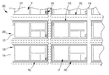
With reference to Figures 2 to 4, we will now describe a first
embodiment of an assembly according to the invention, which is produced
in a card manufacturing method, also in accordance with the invention. The
method of the invention is particularly well suited to manufacturing cards in
batches, i.e. manufacturing several cards simultaneously. The assembly 22
shown partially in Figure 4 includes several electronic modules 2 for
manufacturing several batches of cards. However, it will be noted that the
present invention is not limited to the batch manufacture of cards, but can
also, in a particular variant, apply to card-by-card manufacture, i.e.
individual card manufacture.
CA 02656978 2008-12-15
-10-
Assembly 22 includes a plate 14 that has at least one, at least
partially through aperture 16, and at least one electronic module 2 at least
partially housed in said at least one aperture 16. In the example shown in
Figure 2, plate 14 has a plurality of through apertures 16 and defines as
many frames for electronic modules 2 as there are modules housed in said
apertures 16. The plate defines a positioning structure for the electronic
modules. According to the invention, projecting portions 18 are arranged at
the periphery of each aperture 16. In the variant shown in Figures 2 to 4,
two projecting portions 18 are arranged on two opposite sides of aperture
16, substantially along a diagonal of said aperture. It will be noted,
however,
that there can be any number of projecting parts and they can be arranged
anywhere along the periphery of each aperture 16. Preferably, at least two
projecting portions are provided in each aperture 16. These projecting
portions form stop members for the electronic modules inserted in the
apertures.
Figures 2 and 4 show, in dotted lines 20, the final periphery of each
card obtained from the manufacturing method of the invention, in which
assembly 22 is involved. In a conventional manner, each card obtained is
cut out by means known to those skilled in the art. Figure 3A shows
plate 14 in the cross-sectional plane III-III of Figure 2. The thickness or
height of projecting portions 18 is less than that of plate 14. Projecting
portions 18 are formed before electronic module 2 is brought, in a variety of
manners. These portions can be obtained by hot or cold pressing in a
press. They can also be obtained using an ultrasound head or a head
generating a high frequency electric field. This provides an initial plate 14
of
constant thickness, pierced with apertures 16 that have projecting portions.
Next, the thickness of the projecting portions is reduced, by a tool or head
acting in a localised manner on these projecting portions. This step can be
performed quickly and efficiently using one of the aforementioned means.
In another variant of plate 14, the thickness of projecting portions 18 is
reduced by machining, in particular by using a milling cutter. In another
variant, plate 14 is formed of two layers, laminate welded to each other, the
CA 02656978 2008-12-15
-11-
bottom layer including projecting portions 18, whereas the top layer has
rectangular apertures that match apertures 16 in the projecting portions.
Projecting portions 18 can thus be made by any means known to those
skilled in the art.
Once plate 14 has been made, one electronic module 2, which is
electrically independent of the plate, is inserted into each aperture 16. The
electronic module and all the electrical connections thereof, are made
beforehand. In the example described here, module 2 includes a
substrate 12, which extends into at least some zones at the edge of said
module, beyond the electronic elements 4 to 8 which said module carries.
The dimensions and shape of substrate 12 are such that it has two
zones 24 which are superposed on the two projecting portions 18, when
electronic module 2 is inserted into aperture 16. Thus, substrate 12 abuts
against projecting portions 18, as shown in Figure 3B.
According to the invention, electronic modules 2 are assembled to
plate 14 in a sufficiently rigid manner, firstly, so that electronic modules 2
remain in apertures 16 during the card manufacturing method according to
the invention, and secondly, so that they approximately maintain the initial
position defined when projecting portions 18 are assembled. The electronic
module can be positioned when it is inserted into aperture 16 relative to a
defined reference on plate 14. This positioning of module 2 relative to
plate 14 may concern the module as a whole and thus in particular
substrate 12, or it may concern one particular element of the module, in
particular electronic display 6. This is particularly advantageous, given that
display 6 is, by definition, meant to be visible on one surface of the
finished
card. Precise positioning of the display relative to the contour 20 of the
card
is important for aesthetic reasons, and also functional reasons, when the
display appears through an aperture in a covering layer of the card. When
positioning is required relative to the display, means are provided for
marking electronic display 6 and then inserting module 2 in such a way that
CA 02656978 2008-12-15
-12-
display 6 is in a determined position relative to plate 14, which thus forms a
positioning structure.
Electronic module 2 can be secured to projecting portions 18 in
various ways. By way of example, provided that the materials forming the
two zones 24 of substrate 12 and projecting portions 18 can adhere directly
to each other, said zones 24 are simply heat welded to projecting
portions 18, using thermodes. Module 2 can also be secured to plate 14
using an ultrasound head or other means known to those skilled in the art.
In another variant, an adhesive film is deposited, either on projecting
portions 18, or on zones 24, so as to bond them to each other. In other
variants, substrate 12 is secured to projecting portions by adding drops of
adhesive or a strip of adhesive between the edge of the substrate and the
projecting portions. Any chemical or physical means that assemble
module 2 to the projecting portions in a sufficiently rigid manner can be
used within the scope of the present invention.
A secure assembly is thus obtained, formed of plate 14 and
electronic modules 2, which are housed in apertures 16 of the plate. Two
particular, advantageous features of assembly 22 will be noted:
- firstly, the thickness of module 2 is substantially identical to the
thickness of plate 14, electronic module 2 being entirely housed in the
corresponding aperture 16;
- secondly, a slot 26 remains between module 2 and the edge of
aperture 16, with the exception of the zones where projecting portions 18
are located.
The fact that module 2 is housed entirely inside aperture 16, i.e. in
the thickness of plate 14, means that the manufacture of relatively thin
cards can be better controlled. This means cards that have the smallest
possible increase in thickness relative to the thickness of module 2. The
presence of a slot 26 reduces manufacturing tolerances for pierced plate 14
and modules 2 and also allows substrate 12 to be positioned slightly
differently from one aperture to another, depending upon the position of the
CA 02656978 2008-12-15
-13-
electronic display assembled to the substrate. Moreover, as will become
clear below, slots 26 can then be filled by a resin, which thus provides an
adherent bridge between substrate 12 and the wall of through aperture 16.
This ensures, finally, that electronic module 2 and plate 4 are perfectly
secured to each other, such that, when the finished card is bent or
subjected to other stress, electronic module 2 follows the deformation of
plate 14 properly. This prevents the edges of substrate 12 of module 2
marking the external surfaces of the finished card and thus damaging the
aesthetic appearance of the card. It will be noted that the material used, in
particular for making substrate 12, is selected so that it can withstand a
certain amount of elastic deformation and can allow electronic module 2 to
be bent, when the card is subjected to stress, particularly within the scope
of tests carried out to ensure compliance with the relevant standards.
A first alternative embodiment is shown in Figure 5, which shows a
single aperture 16 of a plate 14, which here has approximately the
dimensions of a single card. This simplified diagram, which is also used in
Figures 6 and 8, is in no way restrictive, and describes an assembly 30,
which is similar to assembly 22 of Figure 4, i.e. for batch manufacturing a
plurality of cards.
The variant of Figure 5 differs in that the projecting portions 18A are
formed in the four corners of aperture 16. The portions thus define
truncated corners in the bottom area of aperture 16. Projecting
portions 18A, which project relative to the generally rectangular shape of
aperture 16, can be made by the same, aforementioned techniques. The
dimensions of module 2 are such that the four corners of substrate 12 are
superposed on the four parts 18A. The electronic module is assembled to
plate 14 in a similar manner to the previously described variant.
Figure 6 shows a second alternative embodiment of the assembly
according to the invention. This alternative is characterized in that it
provides a step 34, which forms an intermediate level against which two
lateral zones 36 of substrate 12 abut, along two opposite edges of
CA 02656978 2008-12-15
-14-
rectangular aperture 16. Steps 34 can be formed in a similar manner to the
projecting portions described in the other variants. The electronic module is
assembled to plate 14 by welding or bonding, or by any other physical or
chemical means available to those skilled in the art.
Figures 7A and 7B show an assembly according to a third variant of
the first embodiment. Frame 14 includes a plurality of apertures 16. The
peripheral area of each aperture has at least one notch 38 or preferably at
least two notches 38. Each notch defines a small circular step. Electronic
module 2 has projecting portions 40 at the edge thereof, which are partially
superposed on notches 38 when module 2 is inserted in aperture 16. These
projecting portions 40 rest on the small circular steps 38. Module 2 is
assembled to plate 14 via zones 40, which are either welded, or bonded in
notches 38. In a particular variant, the notches are sized such that
projecting zones 40 have to be forcibly pushed into these notches, which
secures electronic module 2 to plate 14. However, this latter variant has the
drawback of requiring substrate 12 and notches 38 to be machined very
precisely in the peripheral area of each aperture 16. It will be noted that
the
first and third variants can be combined, with projecting portions 18 then
being superposed on projecting zones 40.
The various variants of the first embodiment of an assembly
according to the invention, which have been described up until now, are
characterized in that distinct zones on the edge of the electronic module, in
particular on the substrate, are superposed on corresponding peripheral
areas of the plate aperture, which houses said electronic module. The
thickness of these peripheral areas is preferably smaller than that of the
pierced plate. According to the invention, said edge zone and said
peripheral area, which is superposed thereon, are assembled to each other
so that the electronic module is secured in the plate aperture. The edge
zone of the electronic module can directly abut against the corresponding
peripheral area or be connected thereto via a resin film. Material
connections are thus created between the electronic module and the
CA 02656978 2008-12-15
-15-
pierced plate by means of specific zones on the edge of the electronic
module, located opposite corresponding peripheral zones of the aperture, in
which the electronic module is arranged.
Figure 8 shows a fourth, particular variant of the first embodiment of
an assembly of the invention. Assembly 44 is formed by a frame 14 that
includes at least one aperture 16, which is separated into two secondary
apertures by a crossbeam 46 whose thickness is less than that of plate 14.
One could say that aperture 16 has two secondary apertures or equally that
there are two apertures separated by a relatively narrow crossbeam.
Electronic module 2 is arranged so that there are no electronic elements in
a central area of substrate 12, which is superposed on crossbeam 46 once
module 2 has been inserted in aperture 16. Module 2 is assembled to
plate 14 via horizontal member 46, to which module 2 is, for example,
welded or bonded. Other assembling means could be provided by those
skilled in the art.
In all of the variants of the first embodiment of an assembly
according to the invention that have been described, the thickness of the
areas of plate 14 that are peripheral to apertures 16 is preferably smaller
than the thickness of the plate in general. It will be noted that other
variants
with a plate of constant thickness could be envisaged. In such case,
substrate 12 is located above plate 14, with the electronic elements in
aperture 16.
Figure 9 shows a second embodiment of an assembly 50 according
to the invention. The references that were described above will not be
described again in detail here. This embodiment is characterized in that
electronic module 2 is assembled to plate 14 via portions of adhesive
strip 52, in particular two portions. In this embodiment, electronic module 2
is entirely contained within the corresponding aperture 16 and has no parts
superposed on plate 14. The adhesive strip portions 52 define material
connections between each electronic module and the pierced plate. These
portions 52 can be arranged on either side of electronic module 2. In the
CA 02656978 2008-12-15
-16-
example of Figure 9, these portions 52 form a bridge between substrate 12
of module 2 and the peripheral area of aperture 16. These portions are
arranged on the opposite side to the electronic elements carried by
substrate 12. This example is in no way restrictive.
This second embodiment is characterized generally by the
arrangement of strips formed of distinct material elements forming bridges
between the edge of the electronic modules and the corresponding
peripheral areas of the apertures housing the electronic modules. An
"adhesive strip portion" means generally a strip portion with a surface that
adheres both the plate 14 and to substrate 12. The adherence must be
sufficient to hold the electronic module in the corresponding aperture 16
during transport and handling of assembly 50, and also during the steps of
the card manufacturing method, in which this assembly 50 is produced as a
constituent element in the batch of simultaneously manufactured cards.
Figure 10 shows an advantageous variant of the second embodiment
of an assembly 56. The material connection or bridge between the
electronic module and the peripheral area of aperture 16 in plate 14 is
achieved here via self-adhesive discs 58. The peripheral area of each
aperture has notches 60 defining two small intermediate steps. The parts of
self-adhesive discs 58 superposed on plate 14 are arranged inside these
notches 60 in order to avoid creating any excessive thickness relative to
frame 14. The depth of notches 60 can be relatively small, at least equal to
the thickness of disc 58, or, conversely, their depth can be relatively large
but less than the thickness of frame 14. The references that have already
been described are not all described again here.
Figure 11 shows a third embodiment of an assembly according to the
invention. This assembly 62 also includes a pierced plate 14 and electronic
modules 2 arranged in apertures 16. These modules 2 are assembled to
plate 14 here by heat-reactivatable adhesive wires 64. These heat-
reactivatable adhesive wires 64 pass through plate 14 and, in particular,
apertures 16. Each heat-reactivatable adhesive wire 64 is arranged to
CA 02656978 2008-12-15
-17-
adhere to plate 14 and to the modules 2 through which it passes. In the
example shown in Figure 11, each electronic module 2 is held in the
corresponding aperture 16 by two wires 64 arranged in proximity to two
opposite edges of the module. The heat-reactivatable adhesive wire 64 can
be a wire made of synthetic or natural material, or covered with adhesive. In
another variant, the wire itself is formed by a solid resin, which can be made
to adhere by applying heat or ultra-violet light. Of course, in another
variant,
an adhesive strip that passes through apertures 16 can form wire 64. In
another variant, the heat-reactivatable adhesive wires could pass grooves
made in plate 14 between two adjacent apertures 16, to prevent the wires
causing excessive thickness relative to plate 14.
Heat-reactivatable adhesive wires 64 can be added before or after
the electronic modules, depending upon the arrangement anticipated.
Likewise, the heat-reactivatable adhesive wires can be provided on the side
of substrate 12 opposite the electronic elements carried by the substrate, as
shown in Figure 11, or located elsewhere, relative to substrate 12, on the
same side as the electronic elements. The heat-reactivatable adhesive wire
can adhere either to substrate 12 or to some of the electronic elements
above which it is arranged. Those skilled in the art will understand that the
possible variants are numerous. The assembly method here comprises an
element that adheres to the electronic module and to plate 14 and passes
through spaces 16 from a peripheral area to another peripheral area of
each aperture 16. Figure 11 shows the heat-reactivatable adhesive wires
parallel to one edge of rectangular apertures 16, but the wires could very
well be arranged obliquely, particularly along a diagonal direction of said
apertures 16.
Figures 12 to 15 show two variants of a fourth embodiment of an
assembly according to the invention. The references that have already
been described previously will not be described again here in detail. This
fourth embodiment differs in that electronic modules 2 are assembled to
plate 14 by introducing a resin in slot 26 between module 2 and the
CA 02656978 2008-12-15
-18-
corresponding aperture 16. In the variant shown in Figures 12 and 13, the
adhesive is introduced, for example by using a syringe, into slot 26 so that a
small strip of adhesive 70 forms an adherent bridge between the lateral
wall 17 of aperture 16 and the edge of substrate 12 of the electronic
module. This strip of adhesive can be added once the electronic module
has been placed in the corresponding aperture in the plate or before the
module is brought. In this latter case, a strip of adhesive is applied against
lateral wall 17 of aperture 16. The strip of adhesive can be added in a
viscous liquid state or in a paste like state, or even in a solid state and
then
made soft or viscous by applying heat. Strip 70 can be formed by any resin
that adheres sufficiently well to frame 14 and the electronic module, in
particular to the substrate 12 thereof, to hold the electronic module in the
corresponding aperture and thus enable assembly 68 to be handled,
without the electronic modules coming out of their respective apertures. The
material connection made beforehand between the electronic module and
plate 14 is important for holding the electronic module in a given position
during the initial handling operations and also during the various steps of
the method according to the invention, which will be described below.
The variant of Figures 12 and 13 is characterized in that the strip of
resin 70 defines a small bridge in slot 26, i.e. between the edge of
substrate 12 and the lateral surface 17 of plate 14. This obviously does not
mean that resin strip 70 cannot also extend partly over one or other of the
top or bottom surfaces of substrate 12 and also over the top surface of
plate 14. However, it will be noted that, preferably, the resin for securing
the
module is entirely inside aperture 16 and does not therefore cause any
excessive thickness relative to the plate.
The variant shown in Figures 14 and 15 differs in that the
assembly 72 includes drops of resin for securing electronic elements 2 to
plate 14. These drops 74 are preferably added to the side of substrate 12
where the electronic elements are arranged. The drops of resin 72 form a
joint essentially between the lateral wall 17 of aperture 16 and the top
CA 02656978 2008-12-15
-19-
surface of substrate 12. This does not, however, mean that drop 74 flows
into slot 26. The two variants of this fourth embodiment of an assembly
according to the invention are thus relatively close to each other. In this
fourth embodiment, a resin is applied locally to create a bridge or joint
between the electronic module and the peripheral area of the corresponding
aperture. This bridge or join is preferably located inside aperture 16 so that
it does not cause any excessive thickness relative to the thickness of
frame 14, which is approximately equal to the maximum thickness of
electronic module 2.
It will be noted that the resin can be applied over several distinct
edge zones of module 2. In Figures 12 and 14, the resin is only deposited in
two diametrically opposite zones. Evidently, more zones could be provided,
in particular, four zones approximately at the four corners of aperture 16. It
will also be noted that the distinct zones can be relatively short as shown in
Figures 12 and 14, or extend over a longer distance, for example, along the
two small sides of rectangular aperture 16.
In all of the embodiments of the assembly according to the invention
described above, the electronic module can have various configurations.
This electronic module can have electronic elements on both sides of
substrate 12 so that the substrate 12 is located in the median area of the
corresponding aperture. Some elements can also be arranged in apertures
in substrate 12 or at the periphery thereof, to prevent their respective
thickness being added. In this latter case, it is also possible for an
electronic
element to pass through the substrate and come out of both sides of the
substrate. Preferably, the thickness of plate 14 is approximately identical to
the thickness of the electronic module; but this is not a compulsory
requirement. Some elements, in particular an electronic display, have a
greater thickness than that of plate 14. Finally, it will be noted that
various
embodiments and/or various variants could be combined with each other.
CA 02656978 2008-12-15
-20-
Two main variants of an intermediate product produced during the
card manufacturing method according to the invention will be described
below with reference to Figures 16 and 17.
The intermediate product 80 shown in Figure 16 is formed by an
assembly according to the invention, said assembly including a pierced
plate 14 and electronic modules housed in corresponding apertures 16.
Substrate 12 of module 2 rests abutting against projecting parts arranged at
the periphery of apertures 16, as described with reference to the first
embodiment of an assembly according to the invention. Initially, electronic
modules 2 and pierced plate 14 are assembled to each other by an
adherent film provided between the projecting parts of plate 14 and
substrates 12 of the electronic modules. In another variant, modules 2 are
secured to plate 14 by adding drops of resin or strips of resin, in particular
in the slot remaining between substrate 12 and wall 84. It will be noted in
Figures 16 and 17 that the example chosen for the assembly according to
the invention is given by way of non-limiting illustration. In fact, any
assembly according to the invention can form an intermediate product by
adding a filling material 82 in the space remaining in apertures 16. In the
variant of Figure 16, the filling material 82 approximately fills each
aperture 16, without, however, covering the top and bottom surfaces of
plate 14, or the surfaces of electronic display 6 that have the same
thickness as plate 14. Filling material 82 fills at least most of the space
remaining in apertures 16. This filling material is added in viscous liquid
form and inserted in the apertures by various means available to those
skilled in the art, in particular by casting pouring or any other technique
known to those skilled in the art. It will be noted, in particular, that it is
possible to envisage introducing filling material 82 by an injection
technique,
by pressing the mould cover on plate 14, the cover mastering the top
surface of electronic display 6 during injection. One variant can be
envisaged wherein electronic display 6 is also covered by the filling
material, which is then transparent. Once again, the examples given are in
no way restrictive. In the variant of Figure 16, the filling material is added
CA 02656978 2008-12-15
-21 -
entirely through the top surface of frame 14, i.e. on the opposite side of
substrate 12 to electronic module 2.
Filling material 82 can be formed by various suitable materials, which
preferably have some elasticity once they have solidified. Preferably filling
material 82 has a good adherence with the lateral walls of openings 16. In
particular, a synthetic or natural resin forms material 82. By way of example,
material 82 can be a polyurethane resin or a PVC resin. Material 82 could
also be formed by an adhesive that hardens at ambient temperature or
reacts, for example, to ultraviolet light (UV). In another variant that could
be
envisaged, material 82 could be formed by a gel or silicon-based material.
The intermediate product 86 shown in Figure 17 differs from that of
Figure 16 in that filling material 82 is formed by a resin that covers at
least
the top surface 88 of plate 14, i.e. the surface on the side of which resin 82
was introduced. In the example of Figure 17, resin 82 also covers bottom
surface 89 of plate 14 and module 2, in particular, substrate 12. In another
variant, plate 14 and the electronic modules are placed on a work surface
or a worksheet as in the case of Figure 16, and the resin is only introduced
slowly, from above, into the space remaining in apertures 16. In such case,
only top surface 88 of plate 14 and the top surface of display 6 will be
covered. If electronic display 6 is covered by resin 82, this resin 82 will
obviously be sufficiently transparent to allow the display to be read. As in
the example of Figure 16, electronic circuit 4 is covered by resin 82.
Once the resin has been added and distributed in apertures 16, a
step is provided for solidifying the resin to form the intermediate product.
In
the example of Figure 17, the assembly according to the invention is
embedded in resin 82. However, in the example of Figure 16, resin 82 does
not define a through layer, but it is localised essentially in apertures 16 of
plate 14. In Figures 16 and 17, the top surface of the solidified resin is
slightly rippled, i.e. it has slight variations in thickness. This does not
mean
that the resin was only added by a casting technique, but it can indicate
that, when the resin or filling material solidified, the material may have
CA 02656978 2008-12-15
-22-
shrunk in a non-homogenous manner, given the presence of relatively bulky
electronic elements, formed of various materials. Thus, the non-flat surface
of intermediate product 86 can also result from a method wherein the resin
is spread using a roller or blade, and even in the case where the resin is
injected or spread in a press with flat surfaces. The intermediate product 86
can already be used to form a card or electronic token once it has been cut
out, but its surface state can be improved within the scope of a method
according to the invention, which will be described below.
Figure 18 shows an alternative embodiment of the intermediate
product. This variant is characterized in that two worksheets are also
provided on either side of the assembly according to the invention, i.e.
covering the top and bottom surfaces of the resin layer. These worksheets
104 and 106 thus have poor adherence to resin 82 and facilitate the
manufacture of the intermediate product. In fact, the resin is not then placed
in contact with the surfaces of the manufacturing installation for the
intermediate products according to the invention. The worksheets are
removed once the resin has solidified. In another variant, a thin plastic film
is provided on each side of the resin, which adheres securely to the resin.
This film remains in the cards manufactured in accordance with the method
described below.
With reference to Figure 19, we will describe below a method of
manufacturing at least one card according to the invention. The steps in this
method include:
- making an intermediate product according to the invention, for
example intermediate product 80 of Figure 16, or intermediate product 86 of
Figure 17;
- depositing a resin over at least one of the top and bottom
surfaces of the intermediate product;
- applying pressure on the resin deposited on the intermediate
product to spread the resin out and make said bottom and/or said top
surface of the intermediate product level, said resin then being in a non-
CA 02656978 2008-12-15
-23-
solid state and preferably viscous liquid, to compensate for any variations in
thickness in the intermediate product.
Figure 19 shows a plurality of cards that are batch manufactured in
accordance with the method described below. After intermediate product 86
was made, two resin layers 92 have been added on either side of
intermediate product 86, in addition to two external solid layers 94 and 96.
Using a press, pressure is applied against external layers 94 and 96 so as
to form a plurality of cards 90. The references that have already been cited
will not be described again here in detail. If the intermediate product
includes two external plastic films, the resin is then deposited above and
the films are covered with resin on both sides.
It will be noted that there are various possible variants as regards the
addition of resin 92 on either side of intermediate product 86. A first main
variant consists in adding the resin in a viscous liquid state, either before
or
simultaneously with the addition of external layers 94, 96. The card
according to the invention can be formed for example in a press with flat
surfaces in which the various elements are placed, or using press rollers
known to those skilled in the art. Resin 92 can be identical to the filling
material or resin 82, used to form the intermediate product. However, a
different resin that is suited to application in thin layers could very well
be
selected for layers 92. Moreover, a resin 92 that is particularly stable and
has no significant shrink during solidification, will preferably be selected.
As is clear from Figure 19, intermediate product 86 has a slightly
rippled top surface. Resin 92 is distributed when pressure is applied so as
to fill in the ripples in the intermediate product, to form a card, or a
plurality
of cards 90, whose external layers 94 and 96 have a perfectly flat surface.
Manufacturing by adding the resin or filling material in two steps results in
cards that have a given thickness and thus overcomes the flatness
problems encountered in the manufacture of cards that have relatively large
electronic modules or elements inside, in particular electronic elements
whose thickness is variable, which cause variable resin thickness inside the
CA 02656978 2008-12-15
-24-
card. The resin can be added to the intermediate product and pressure can
be applied above in several successive steps. Thus, during the first
application of resin, two worksheets are preferably used, and then removed
once resin layers 92 have solidified. A second resin layer can then be
added above to further improve the flatness of the card. As already
mentioned, a multi-layered structure with thin plastic films between two
depositions of thin resin layers, could also be provided.
According to a second main variant, the resin layers 92 are added in
the form of solid resin sheets, which are then at least partially melted prior
to or simultaneously with the application of pressure to form the finished
cards. The resin sheets are thus sufficiently soft and easily deformed for the
resin to be able to spread and fill the surface unevenness of the
intermediate product 86, in order to form a high quality flat card. Heat can
be applied by various means and, in particular, via the actual press. Finally,
resin 92 can also be solidified in various ways, depending upon the features
of the resin. The resin can solidify at ambient temperature, or by other
means known to those skilled in the art, particularly by a chemical reaction
or polymerisation with thermosetting materials.
It will be noted that the finished card 90 can include several external
layers and transparent protective layers, for example, to protect any printing
performed on layer 94 or 96. Generally, any intermediate product and any
card obtained within the scope of the present invention, can then be
laminated with a variable number of plastic layers, without using any
additional resin. An intermediate layer that has been laminated with external
layers in this way can form finished cards after the cutting operation.
With reference to Figures 20 to 22, we will describe another
implementation of the card or intermediate product manufacturing method
according to the invention. In this implementation, one may take any
assembly according to the invention, formed of a pierced plate 14 and
electronic modules, in particular a display 6 and an electronic circuit 4
mounted on a substrate 12. As in Figures 16 and 17, the electronic display
CA 02656978 2008-12-15
-25-
is arranged in an aperture of substrate 12 or at the periphery thereof. It is
secured to the substrate by connecting pins or other connecting or securing
means. This assembly according to the invention is provided with a resin
98, in a viscous liquid state, between two solid layers 94 and 96,
respectively 104 and 106 in an installation provided with press rollers 100
and 102, between which the various elements are continuously introduced.
Rollers 100 and 102 preferably rotate freely and the assembly formed of the
electronic modules and the pierced plate, and the external layers, are
pulled. This implementation is not restrictive, but has the advantage of
allowing the assembly according to the invention and the external layers in
contact with press rollers 100 and 102 to move forward in an identical way.
Resin 98 is preferably added to bottom layer 94, or respectively top layer
104 and over the assembly according to the invention. This is in no way
restrictive and any other way of adding the resin that allows the electronic
assembly to be properly embedded or coated could be used by those
skilled in the art. The installation supports have been shown entirely
schematically and do not form any particular feature of the method of the
invention.
It will be noted that press rollers 100 and 102, and the arrangement
thereof in the card manufacturing installation, have been shown
schematically. It is possible to provide several pairs of press rollers
arranged one after the other or other similar means of pressure, for
example a continuous press fitted with a conveyor belt. These pairs of
rollers can have different diameters and the distance between the rollers of
one pair can also be different. In particular, the distance between the press
rollers could decrease in the direction of movement of the elements that
pass through the press rollers. Thus, the thickness gradually decreases
between external layers 94 and 96, or 104 and 106 respectively. This
enables the resin 98 to be better distributed to obtain improved flatness for
the manufactured cards.
CA 02656978 2008-12-15
-26-
Means other than press rollers could be provided, for example blades
for spreading out the resin and distributing it in the remaining spaces in the
apertures in the pierced plate and on either side of the assembly of the
invention.
Figure 21 shows a batch of cards obtained by the method described
above. Cards 108 thus include an electronic module connected to a pierced
plate 14 and coated with resin 98. These cards include two external solid
layers 94 and 96, which have approximately flat surfaces. These layers 94
and 96 adhere properly to resin 98, so that they form part of the finished
cards. In a known manner, each card is cut out of the batch of
simultaneously manufactured cards using a cutting tool or by means known
to those skilled in the art, particularly using a jet fluid.
Figure 22 shows an intermediate product or a batch of cards 110
obtained by the manufacturing method described with reference to
Figure 20. Here, solid layers 104 and 106 form worksheets that do not
adhere well to resin 98 so that these sheets 104 and 106 are removed once
resin 98 has solidified. An intermediate product, or batch of cards is thus
obtained, whose body is formed by resin 98, the external surfaces of the
resin then defining the external surfaces of the product obtained. According
to various variants, other external layers can be subsequently added, by
laminating either side of the intermediate product 110. Likewise, the
cards 108 shown in Figure 21 can also receive other external layers, in
particular a printing layer and a final transparent protective layer. The
cards
can be individually cut before or after these additional layers are added.
In another implementation of the method described here, the
intermediate product or cards can be formed in a press that has flat
surfaces. All of the elements are added between these surfaces before any
pressure is exerted to form the intermediate products or approximately flat
cards. It will be noted that it is possible, firstly, to use press rollers and
then
to place the product obtained in a press with a flat surface until the resin
solidifies. It will be noted finally, that resin 98 is preferably added in a
CA 02656978 2008-12-15
-27-
viscous liquid state. However, in a variant, it is possible to add the resin
or
any other filling material in a solid state and then to melt it so that it can
then fill the remaining spaces in the apertures in pierced plate 14 and thus
form compact and substantially full cards, i.e. cards that have a relatively
low level of residual air.