Note : Les descriptions sont présentées dans la langue officielle dans laquelle elles ont été soumises.
CA 02657154 2009-01-07
WO 2008/008952 PCT/US2007/073458
HIGH-SPEED SIGNAL TESTING SYSTEM HAVING OSCILLOSCOPE FUNCTIONALITY
RELATED APPLICATION DATA
[0001] This application claims the benefit of priority of U.S. Provisional
Patent Application
Serial No. 60/830,797, filed on July 14, 2006, and titled "Signal Integrity
Measurement System
And Method Using A Predominantly Digital Time-Base Generator," which is
incorporated
herein by reference in its entirety.
FIELD OF INVENTION
[0002] The present invention relates generally to the measurement of high-
speed digital data.
More particularly, the present invention is directed to a high-speed signal
testing system having
oscilloscope functionality.
BACKGROUND
[0003] Digital communication speeds within semiconductor components, between
semiconductor components, and between boards and cabinets continue to
increase. As speeds
increase, testing digital signals does not only involve logic (pattern)
testing, but also requires
analog parametric testing. With increased speeds, the analog shape of the
voltage waveform
representing the binary digital data is important. Poor analog parameters such
as too long a rise
time or too small a voltage swing may result in long term issues that are not
uncovered using
quick pattern tests. Conversely, analog parameter testing is also useful when
debugging failures
in logic or pattern tests. Such failures can be caused by systematic phenomena
that manifest
themselves in waveform shape or timing jitter.
[0004] In the present state of the art, separate pieces of equipment are often
required to perform
logic testing and analog parametric testing, respectively. For example, a
logic analyzer or a bit-
error-rate tester (BERT) is used for pattern testing and an oscilloscope or
jitter analyzer is used
for eye diagram testing or jitter testing. As the need to test high-speed
digital signals proliferates
more into large pin-count devices or circuits, there arises a need to combine
some of the
capabilities of various pieces of equipment. There is also a need to integrate
such capabilities in
devices or in small form factors that can fit on application devices or on
application boards. For
example, a test-related module or component can be placed on a system to
perform the digital
testing functions. Many high-speed serial receivers now contain a pattern
checker for the purpose
1
CA 02657154 2009-01-07
WO 2008/008952 PCT/US2007/073458
of digital testing. Adding oscilloscope capability to this basic pattern
checking capability is
highly desired, but not trivial.
[0005] By way of example using commercial test equipment, enabling a BERT or
logic analyzer
to perform eye diagram analysis simplifies testing and provides enhanced
coverage with one
piece of equipment instead of two. Such equipment already exists. However,
given the
contradicting requirements between pattern testing and analog parametric
testing, creating such
dual-function equipment entails intricate modifications to the basic
architecture of the equipment
that limits scalability. In particular, to enable a BERT to generate an eye
diagram, the former is
modified in two main ways. First, analog delay line circuitry is introduced
that can delay a data
signal or a clock signal, or both, by very small amounts (fraction of data
pattern unit interval).
The delay line circuitry is area-consuming, bandwidth-limited, and difficult
to calibrate. It
becomes unmanageable when several test channels are required, as is the case
in modern
applications or applications in which the pattern tester is integrated within
a system.
[0006] The other modification that is required involves the front-end capture
electronics.
Specifically, logic testing merely requires a voltage comparator at the front
end of the equipment
whereas a measurement such as an eye diagram requires a more complex circuit.
To modify a
BERT to perform eye diagram measurement, engineers create a window comparator
(two or
more voltage comparators with similar but slightly offset threshold levels) to
detect a transition
through a very narrow voltage plane and associated time point. Alternatively,
instead of
deploying two or more comparators to perform a window comparison, another
implementation
involves two slightly delayed strobes applied to a single voltage comparator,
the delay being a
small fraction of the data pattern unit interval. This approach is again
complicated and difficult to
implement at very high speeds.
SUMMARY OF THE DISCLOSURE
[0007] One aspect of the present invention is a system for testing a high-
speed repeating data
signal, comprising: a time-base generator responsive to a reference clock
signal so as to generate
a high-speed repeating signal; a one-bit voltage digitizer for digitizing the
high-speed repeating
data signal into a digitized signal as a function of the high-speed repeating
signal; a digital
comparator for comparing the digitized signal to a selected digital value and
outputting
comparator results as a function of the high-speed repeating signal; a bit-
shift and frequency-
2
CA 02657154 2009-01-07
WO 2008/008952 PCT/US2007/073458
divider block responsive to the high-speed repeating signal so as to produce a
slowed clock
signal; a sub-sampler for sub-sampling the comparator results as a function of
the slowed clock
signal so as to output sub-sampled results; a modulo N address counter for
providing write
addresses as a function of the high-speed repeating signal; and an
accumulation memory for
storing ones of the sub-sampled results as a function of the slowed clock
signal and
corresponding respective ones of the write addresses.
[0008] Another aspect of the present invention is a system for testing a high-
speed repeating data
signal, comprising: oscilloscope circuitry that includes: a time-base
generator responsive to a
reference clock signal so as to generate a high-speed repeating signal; a one-
bit voltage digitizer
for digitizing the high-speed repeating data signal into a digitized signal as
a function of the
high-speed repeating signal; a reference pattern memory for storing a
reference bit pattern having
a length B; a selector for selecting between the reference bit pattern and a
constant bit value so as
to output a selected digital value; a digital comparator for comparing the
digitized signal to the
selected digital value and outputting comparator results as a function of the
high-speed repeating
signal; a bit-shift and frequency-divider block responsive to the high-speed
repeating signal so as
to produce a slowed clock signal, the bit shift and frequency divider block
divides the high-speed
repeating signal by B; a sub-sampler for sub-sampling the comparator results
as a function of the
slowed clock signal so as to output sub-sampled results; a modulo N address
counter for
providing write addresses as a function of the high-speed repeating signal;
and an accumulation
memory for storing ones of the sub-sampled results as a function of the slowed
clock signal and
corresponding respective ones of the write addresses.
[0009] Still another aspect of the present invention is a method of
implementing an oscilloscope
to analyze a high-speed data signal, comprising: digitizing the high-speed
data signal into a one-
bit digitized signal in response to a repeating time-base signal having a time-
base span N;
comparing the one-bit digitized signal to a constant bit value in response to
the repeating time-
base signal so as to generate comparator results; dividing the repeating time-
base signal so as to
create a slowed clock signal corresponding to high-speed data period; sub-
sampling the
comparator results in response to the slowed clock signal so as to output sub-
sampled results;
generating modulo N write addresses as a function of the repeating time-base
signal; and storing
3
CA 02657154 2009-01-07
WO 2008/008952 PCT/US2007/073458
ones of said sub-sampled results in a memory in response to the slowed clock
signal and
corresponding respective ones of the write addresses.
BRIEF DESCRIPTION OF THE DRAWINGS
[0010] For the purpose of illustrating the invention, the drawings show
aspects of one or more
embodiments of the invention. However, it should be understood that the
present invention is
not limited to the precise arrangements and instrumentalities shown in the
drawings, wherein:
FIG. 1 is a high-level schematic diagram of a prior-art digital pattern
tester;
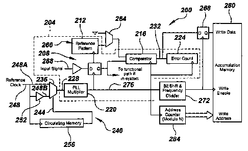
FIG. 2 is a high-level schematic diagram of a digital pattern testing system
of the present
disclosure that includes oscilloscope functionality;
FIG. 3 is a timing diagram illustrating the functioning of frequency divider
block of the digital
pattern testing system of FIG. 2 for the frequency divider value B equal to
11;
FIG. 4 is a diagram illustrating the contents of the accumulative memory of
the digital pattern
testing system of FIG. 2 for a one-bit digitized waveform;
FIG. 5 is a diagram illustrating a single sequence of bits stored in the
accumulative memory of
the digital pattern testing system of FIG. 2, the sequence of bits resulting
from setting the
threshold voltage of the receive comparator at a fixed value and running the
time-base generator
for a particular data pattern bit;
FIG. 6 is a diagram illustrating multiple sequences of bits stored in the
accumulative memory of
the digital pattern testing system of FIG. 2, the multiple sequences of bits
resulting from
sweeping the threshold voltage of the receive comparator at differing fixed
values and running
the time-base generator at the differing values for a particular data pattern
bit;
FIG. 7 is a timing diagram illustrating the operation of the digital pattern
testing system of FIG. 2
for a bit-pattern length of 5;
FIG. 8A is a plot of waveform voltage versus time of an exemplary digital bit
stream as
outputted using the oscilloscope functionality of a digital pattern testing
system of the present
disclosure; FIG. 8B is a zoomed-in plot of waveform voltage versus time for a
rising edge of a
bit transition as outputted using the oscilloscope functionality of a digital
pattern testing system
of the present disclosure; FIG. 8C is a zoomed-in plot of waveform voltage
versus time for a
4
CA 02657154 2009-01-07
WO 2008/008952 PCT/US2007/073458
falling edge of a bit transition as outputted using the oscilloscope
functionality of a digital
pattern testing system of the present disclosure; FIG. 8D is a zoomed-in plot
of waveform
voltage versus time for a constant high bit value as outputted using the
oscilloscope functionality
of a digital pattern testing system of the present disclosure; FIG. 8E is a
zoomed-in plot of
waveform voltage versus time for a constant low bit value as outputted using
the oscilloscope
functionality of a digital pattern testing system of the present disclosure;
and
FIG. 9 is an overlay plot of waveform voltage versus time for two rising
transitions that exhibit
data-dependent jitter as outputted using the oscilloscope functionality of a
digital pattern testing
system of the present disclosure.
DETAILED DESCRIPTION
[0011] FIG. 1 shows a prior-art digital pattern tester 10 for testing logical
integrity of an input
signal 14 input into the tester. As mentioned in the Background section above,
tester 10 could be
part of the design of a high-speed digital communications device (not shown),
or it could be a
standalone piece of equipment, such as a BERT or logic analyzer. The front-end
of tester 10 is a
voltage comparator 18 that "slices" the voltage of incoming signal 14 and
recovers a logical
value from it. The logical value is "1" when the input signal is larger than
the voltage threshold
of comparator 18 and "0" otherwise. Using a digital comparator 22, the logical
value is then
compared, bit for bit, to a reference pattern 26 stored in an onboard memory
30. An error
counter 34 keeps track of the number of mismatches between the logical values
derived from
input signal 14 on the one hand and the corresponding respective bits of
reference pattern 26 on
the other.
[0012] Digital comparator 22 is clocked by an onboard clock signa138 that is
centered at the
middle of the data bit that is being compared. This minimizes the likelihood
of a sampling error.
Depending on the architecture, the centering operation either happens with
delay lines (not
shown) on the clock signal or with a phase tracking circuit (not shown), such
as a clock-and-data
recovery (CDR) circuit. The latter scenario is more common in in-system
applications. Also
possibly included is a digital pattern alignment block (not shown) that shifts
reference pattern 26
until the least amount of errors is observed. In any case, reference clock 42
provided to tester 10
can be at a low frequency, with subsequent multiplication, typically using a
phase-locked loop
CA 02657154 2009-01-07
WO 2008/008952 PCT/US2007/073458
(PLL) multiplier 46, to the target high-speed frequency. In one example,
multiplication can
increase a 100 MHz clock signal to a 5 GHz sampling signal.
[0013] Referring now to FIG. 2, this figure shows an exemplary digital pattern
testing
system 200 that includes an oscilloscope feature that enables the capture of
oscilloscope traces of
transition or non-transition bits. As will be readily seen by visually
comparing FIGS. 1 and 2
with each other, exemplary testing system 200 is based on the design of
pattern tester 10 of
FIG. 1, the major components of which are located within the dashed outline
204. That is, like
tester 10 of FIG. 1, testing system 200 of FIG. 2 includes a front end voltage
comparator 208, a
reference pattern memory 212, a digital comparator 216, a frequency-scaling
PLL multiplier 220,
and an error counter 224. As can further be seen comparing FIGS. 1 and 2 to
each other,
additions made to the conventional tester components within dashed outline 204
of FIG. 2
include additions to the input 228 of PLL multiplier 220 and to the output 232
of digital
comparator 216. As will be seen, both of these modifications are digital in
nature, and can be
implemented without much of the risks described earlier using conventional
methods.
[0014] In the first modification, input 228 of PLL multiplier 220 is preceded
by a
multiplexer 236 and other components as described below to provide a high-
frequency time-base
generator 240, which may be, for example, any one of the time-base generators
described in U.S.
Patent Application Serial No. 11/776,825, filed on July 12, 2007, and titled
"Signal Integrity
Measurement Systems And Methods Using A Predominantly Digital Time-Base
Generator,"
which is incorporated by reference herein for all that it discloses relative
to time-base generators.
In the example shown, multiplexer 236 is responsive to a selection signa1244
that continually
selects between two inputs, which in this case are two versions of an incoming
reference clock
signa1248, an undelayed version 248A and a coarsely delayed version 248B that
is delayed using
a coarse delay 252. Coarse delay is defined as any delay that is substantially
larger than the
minimum delay that can be reliably constructed using conventional technology.
Typically, such
delay is equivalent to minimum bit period in a high speed communications
device. In general and
as described in the '825 application, however, the selectable input signals to
multiplexer 236 may
be any two or more clock signals that are coarsely delayed relative to one
another. In this
example, selection signa1244 comes from an onboard circulating memory 256 that
is clocked by
incoming reference clock 248. The combination of PLL multiplier 220,
multiplexer 236, coarse
6
CA 02657154 2009-01-07
WO 2008/008952 PCT/US2007/073458
delay 252 to create the delayed version 248B of clock signa1248, selection
signa1244, and
onboard memory 256 driving the selection signal constitute a time-base
generator 240 that
replaces any analog delay lines that are required in a conventional system.
The advantage of
using digital logic over analog logic especially in in-system applications are
well known to those
versed in the art.
[0015] In addition to time-base generator 240, to enable oscilloscope
measurement without
implementing a window comparator or a more complicated front-end, the digital
logic down
stream of voltage comparator 208 is modified, for example, as shown in FIG. 2.
First, during
oscilloscope mode, the reference pattern 260 can be replaced by a constant
logical value, such as
0. Selection between the oscilloscope mode and the bit-pattern testing mode
can be facilitated,
for example, by a multiplexer 264 that allows selection between the constant
logical 0 signal and
the output of reference pattern memory 212. Digital comparator 216 can remain
the same as
digital comparator 22 of FIG. 1 for simplicity if desired. Additionally, in
the oscilloscope mode,
error counter 224 may be bypassed and replaced by a sub-sampling flip-flop
268. As will be
described shortly, sub-sampling flip-flop 268 serves the function of locking
onto a single bit in
the high-speed pattern being tested.
[0016] Effectively, when testing system 200 is in oscilloscope mode, the
system is designed to
zoom into a particular edge or other portion of the pattern and analyze it. To
achieve this, sub-
sampling flip-flop 268 is driven by a bit-shift and frequency-divider block
272 responsive to the
output 276 of time-base generator 240. The frequency division of bit-shift and
frequency-divider
block 272 is set to a value equal to the length B of pattern 260. If pattern
260 is a pseudo-random
bit sequence (PRBS) having a pattern length B of 127 bits, the frequency
divider value is 127.
The bit shifting operation of bit-shift and frequency-divider block 272 moves
this slowed-down
clock in single-bit increments, potentially placing it at each of the 127
positions in original
periodic test pattern 260. FIG. 3 shows the operation of bit-shift and
frequency-divider
block 272 (FIG. 2)for a pattern 260A having length B of 11. The 11 shifted
outputs Output 1
through Output B(B=11) of bit-shift and frequency-divider block 272 are
illustrated. Any one of
these outputs is generated at a given time. Intuitively from this figure, sub-
sampling flip flop 268
(FIG. 2) only looks at the digital comparison result every 11 data beats,
instead of every data
beat. It only looks at the comparison result for a single bit in the whole
repeating pattern 260A.
7
CA 02657154 2009-01-07
WO 2008/008952 PCT/US2007/073458
[0017] Referring again to FIG. 2, the output of the sub-sampled comparison
operation may be
accumulated in an accumulation memory 280 having an address counter 284
clocked by time-
base generator 240. The importance of addressing using address counter 284
this way is
described below. For now, its is noted that because division ratio of bit-
shift and frequency-
divider block 272 is equal to pattern length B in FIG. 2, the accumulation
results may arrive into
accumulation memory 280 out of order, but if certain guidelines are followed,
all locations in the
memory will be covered (see below).
[0018] As discussed in detail in the '825 patent application, each time PLL
multiplier 220
toggles its output 276 is slightly delayed. Thus, every time voltage
comparator 208 is clocked, it
strobes the incoming bit stream of input signa1288 at a slightly different
delay. Similarly, every
time sub-sampling flip flop 268 is clocked with the slowed-down clock of bit-
shift and
frequency-divider block 272, it, too, corresponds to a slightly different
delay. If time-base
generator 240 is programmed to generate a constant ramp (see the '825 patent
application for a
description of programming a time-base generator), the output 276 of PLL
multiplier 220 is
constantly advanced or delayed by a fixed amount according to the ramp
behavior. Each entry in
accumulation memory 280 is designed to correspond to a single delay value out
of PLL
multiplier 220. Thus, and referring to FIG. 4, at the termination of one
complete sweep of the
time-base ramp, accumulation memory 280 will contain a time-domain waveform
400
corresponding to whether or not the transition bit being zoomed onto is higher
than the voltage
threshold of voltage comparator 208 (FIG. 2).
[0019] If the threshold voltage of voltage comparator 208 is programmable,
sweeping the
threshold voltage can help generate a complete voltage waveform for a data bit
of interest
without requiring a window comparator or additional strobe circuitry.
Referring to FIGS. 2
and 5, FIG. 5 illustrates the setting of the threshold voltage of voltage
comparator 208 (FIG. 2) to
a fixed value VB and running time-base generator 240 for a bit 500 of interest
of data
pattern 260B. The result is a sequence 504 of ones and zeros that may be
stored in accumulation
memory 280. Incrementing the threshold voltage of voltage comparator 208 and
re-running time-
base generator 240, another sequence of ones and zeros is generated, and it is
added to the
previous set. As the sweep proceeds, a thermometer code like the thermometer
code 600 shown
in FIG. 6 is obtained. Of course, in the exemplary implementation, the values
of the thermometer
8
CA 02657154 2009-01-07
WO 2008/008952 PCT/US2007/073458
code are directly accumulated in accumulation memory 280. It should be noted
that this
operation is different from the operation of generating bit error rate (BER)
contour plots. This
operation is literally a digitization operation of a repetitive voltage
transition. It does not
represent an error count the way a BER does.
[0020] Returning to accumulation memory 280 and time-base generator 240 of
FIG. 2, specific
selection of the length of accumulation memory 280 (and time-base ramp length)
with respect to
repeating pattern 260 under test is required. Most simplistically, if data
pattern 260 being
measured has an even length, the length of accumulation memory 280
(representing the time axis
in the digitization process) is selected to have an odd number of locations.
Conversely, if the
pattern length is odd, the length of accumulation memory 280 (and
corresponding time-base
generator ramp) is even. Referring to FIGS. 2 and 7, FIG. 7 shows an exemplary
test
pattern 260C (FIG. 2), exemplary time delay values 700 outputted by the time-
base generator
240, exemplary memory address values 704, and the order 708 in which the
memory values are
filled. In the figure, pattern 260C has a length B of 5 bits and a bit 712 of
interest. Time-base
generator 240 ramps through its various delays in a duration equivalent to 8
bit-values. As can be
seen, all memory values 704 are eventually filled as long as the sufficient
number of iterations of
the PLL ramp and of the bit stream is sequenced. If the length of accumulation
memory 280 is
not selected properly, aliasing effects occur, and erroneous measurements are
made. In general,
the number of iterations of the time-base ramp or the bit pattern 260C
corresponds to the least
common multiple between the pattern length B and the time-base span N. In the
example of
FIG. 7, the least common multiple between 5 and 8 is 40. So, 8 iterations of
pattern 260C (or 5 of
the time-base ramp) are required. Still referring to FIG. 7, notice how, at
the start 716A of the
timing waveform 716 shown, as PLL multiplier 220 keeps toggling and ramping
its output delay,
it comes across the bit of interest 712 (transition of interest) twice. This
means that voltage
comparator 208 samples that particular bit 712 (transition) with a small delay
at first, then with a
large delay subsequently. In the next iteration 716B of the ramp timing
waveform 716, PLL
multiplier 220 comes across the same transition repetitively again, but each
time it does so, it
does it with a unique one of delay value 700.
[0021] Concerning lengths of accumulation memory 280, the time-base span is
typically in the
order of hundreds of samples (e.g. 512) because it becomes overkill to create
much larger timing
9
CA 02657154 2009-01-07
WO 2008/008952 PCT/US2007/073458
resolution. Length B of bit pattern 260, on the other hand, can be much
smaller (e.g. 5 in the
example above) or much larger (e.g., thousands of bits).
[0022] FIG. 8A shows an example of an output plot 800 of example digital bit
stream 804 as
generated using the oscilloscope functionality of an oscilloscope-enabled
testing system made in
accordance with the present disclosure, such as digital pattern testing system
200 of FIG. 2.
Because of bandwidth limitations and lossy transmission, bit stream 804 shows
slow rise time
and significant voltage noise. These effects are examples of what is being
tested using an
oscilloscope-enabled testing system of the present disclosure. FIG. 8B shows
an example of plot
808 generated by an oscilloscope-enhanced testing system of the present
disclosure, such as
digital pattern testing system 200 of FIG. 2, when the testing system is
zoomed in onto a rising
transition 812. FIG. 8C shows an example of plot 816 generated by an
oscilloscope-enhanced
testing system of the present disclosure, such as digital pattern testing
system 200 of FIG. 2,
when the testing system is zoomed in onto a falling transition 820. FIGS. 8D
and 8E show,
respectively, exemplary plots 824, 828 generated by an oscilloscope-enhanced
testing system of
the present disclosure, such as digital pattern testing system 200 of FIG. 2,
when the testing
system is zoomed in onto constant high and constant low bit values 832, 836,
respectively.
[0023] As can be seen, an oscilloscope-enabled testing system of the present
disclosure has great
utility in identifying problem areas in a digital bit stream. For example,
data-dependent jitter can
easily be extracted since, now, the average arrival time of each transition in
a bit stream is made
available. FIG. 9 shows an example plot 900 containing an overlay of two
rising transitions 904,
908 that exhibit data-dependent jitter. As can be readily seen, transitions
904, 908 occur at
different times. Similarly, histograms on particular edges can be extracted to
learn about jitter
parameters that are non-data-dependent. Finally, all transition edges can be
accumulated together
to generate eye masks or eye diagrams. Those skilled in the art will
understand how to
implement these and other additional oscilloscope related features using the
concepts disclosed
herein.
[0024] Exemplary embodiments have been disclosed above and illustrated in the
accompanying
drawings. It will be understood by those skilled in the art that various
changes, omissions and
additions may be made to that which is specifically disclosed herein without
departing from the
spirit and scope of the present invention.