Note : Les descriptions sont présentées dans la langue officielle dans laquelle elles ont été soumises.
CA 02657509 2009-03-09
-1-
SPECIFICATION
DIFFRACTION GRATING-FABRICATING PHASE. MASK, AND ITS
FABRICATION METHOD
TECHNICAL ART
The present invention relates generally to a diffraction
grating-forming phase mask and its fabrication method, and
more particularly to a phase shift mask for using ultraviolet
laser light to form a diffraction grating in an optical fiber
used for optical communications, etc.
BACKGROUND ART
Optical fibers have brought about breakthroughs in the
globalization of communications to make high-quality and
large-capacity inter-oceanic telecommunications feasible. So
far, it has been known that a Bragg diffraction grating is
provided in an optical fiber by creating a periodic
refractive index profile in an optical fiber core along the
optical fiber, and the magnitude of reflectivity and the
width of the wavelength characteristics of the diffraction
grating are determined by the period and length and the
magnitude of refractive index modulation of the diffraction
grating, whereby the diffraction grating can be used as a
wavelength division multiplexer for optical communications, a
narrow-band yet high-reflection mirror used for lasers or
sensors, a wavelength selection filter for removing extra
laser wavelengths in fiber amplifiers, etc.
However, the wavelength at which the attenuation of a
quartz. optical fiber is minimized and which is suitable for
long-distance communications is 1.55 pm. It is thus required
CA 02657509 2009-03-09
-2-
that the grating spacing be about 500 nm in order to allow
the optical fiber diffraction grating to be used at this
wavelength. At the beginning, it was considered difficult to
make such a minute structure in an optical fiber core; that
is, a Bragg diffraction grating was provided in the optical
fiber core by a sophisticated process comprising a number of
steps, e.g., side polishing, photoresist coating, holographic
exposure, and reactive ion beam etching. For this reason,
much fabrication time was needed, resulting in low yields.
In recent years, however, a method of fabricating a
diffraction grating by irradiating an optical fiber with
ultraviolet radiation to cause a refractive index change
directly in an optical fiber core has been developed. This
ultraviolet irradiation method has been steadily put to
practical use with the advance of peripheral technologies,
because of no need of any sophisticated processes.
Since the grating spacing is as fine as about 500 nm as
mentioned above, this method using ultraviolet light is now
carried out by a two-beam interference process, a writing-
per-point process wherein single pulses from an excimer laser
are focused to make diffraction grating surfaces one by one,
an irradiation process using a phase mask having a grating,
etc.
Regarding the two-beam interference process, a problem
arises in conjunction with the quality of the beams in the
lateral direction, i.e., spatial coherence. A problem with
the writing-per-point process is on the other hand that
strict step control of the submicron order is needed to focus
CA 02657509 2009-03-09
-3-
light on a small point for writing light on many surfaces.
Another problem arises in conjunction with processability.
To solve these problems; attention has focused on the
irradiation process using a phase mask. According to this'
process, a phase mask 21 comprising a quartz substrate
provided on one surface with grooves of given depth at a
given pitch is irradiated with KrF excimer laser light (of
248 nm wavelength) 23 to give a refractive index change to a
core 22A of an optical fiber 22, thereby producing a grating
(diffraction grating), as shown in Fig. 7(a). For a better
understanding of an interference pattern 24 on the core 22A,
the pattern 24 is exaggerated in Fig. 7(a). Fig. 7(b) is a
sectional view of the phase mask 21, and Fig. 7(c) is a
partial top view corresponding to Fig. 7(b). The phase mask
21 has a binary phase type of diffraction grating structure
where the substrate is provided on one surface with grooves
26 having a depth D at a repetition pitch P, with a strip 27
substantially equal in width to each groove being provided
between adjacent grooves 26.
The depth of each groove 26 on the phase mask 21 (the
difference in height between strip 27 and groove 26) D is
chosen such that the phase of the excimer laser light (beam)
23 that is exposure light is modulated by a radian. Thus,
zero-order light (beam) 25A is reduced to 5% or less by the
phase mask 21, and chief light (beam) leaving the mask 21 is
divided into + first-order diffracted light 25B containing at
least 35% of diffracted light and - f-first-order diffracted
light 25C, so that the optical fiber 22 is irradiated with
CA 02657509 2009-03-09
-4-
the + first-order diffracted light 25B and - first-order
diffracted light 25C to produce an interference fringe at a
given pitch, thereby providing a refractive index change at
this pitch in the optical fiber 22.
When the diffracting grating is fabricated in the
optical fiber 22 by interference of + first-order light 25B
and - first-order light 25C using such a phase mask 21,
deposition of foreign matters on the surface of the phase
mask 21 causes defects in the diffraction grating exposed to
light in the optical fiber 22. This in turn gives rise to
noises in the characteristic spectra of the diffraction
grating.
When the optical fiber 22 is irradiated with ultraviolet
radiation 25B and 25C according to such an arrangement as
shown in Fig. 7(a), the covering resin of the optical fiber
22 is sublimated due to exposure to ultraviolet radiation 25B
and 25C, filling up the grooves 26 in the phase mask 21.
This offers a similar defect problem with respect to the
diffraction grating exposed to light in the optical fiber.
A prior grating constituting such a diffraction grating-
fabricating phase mask 21 has a reduced diffraction
efficiency and so shows an about 3% transmittance with
respect to zero-order light 25A because the grooves 26 are of
a rectangular wave shape in.section, as shown in Fig. 7(b).
This zero-order light component 25A makes noises, which in
turn appear in the reflection spectra of the transferred
optical waveguide diffraction grating.
DISCLOSURE OF THE INVENTION
CA 02657509 2009-03-09
-5-
in view of such problems with the prior art as mentioned
above, one object of the present invention is to provide a
diffraction grating-forming phase mask which, even when
foreign matters, resins sublimated from an optical fiber,
etc. are deposited on the surface thereof, makes it unlikely
to introduce defects in the diffraction grating to be formed.
Another object of the invention is to provide a
diffraction grating-fabricating phase mask which can reduce
as much as possible a zero-order light component transmitting
through the phase mask without subjected to diffraction, so
that no noise can be introduced in the reflection spectra of
an optical waveguide diffraction grating obtained by
transfer, and a method of fabricating such a phase mask.
To achieve the aforesaid first object of the invention,
the invention provides a diffraction grating-forming phase
mask comprising a transparent substrate provided on one side
with a grating form of repetitive groove-and-strip pattern
for forming a diffraction grating with interference fringes
of diffracted light through said repetitive pattern,
characterized in that an optically transparent protective
layer is applied over said one side with said repetitive
groove-and-strip pattern formed thereon.
Preferably, the protective layer should comprise a sheet
or film formed of any one of Si02r CaF2, MgF2, ZrO, HfO, and
fluorine resin.
Preferably, the protective layer should be a sheet or
film having a thickness of 0.1 mm to 2 mm.
CA 02657509 2009-03-09
-6-
According to this embodiment of the invention, there is
also provided a diffraction grating-forming phase mask
comprising a transparent substrate provided on one side with
a grating form of repetitive groove-and-strip pattern for
forming a diffraction grating with interference fringes of
diffracted light through said repetitive pattern,
characterized in that an optically transparent material layer
having a refractive index different from that of said
transparent substrate is applied over said one side with said
repetitive groove-and-strip pattern formed thereon by film-
forming means such as evaporation, CVD, sputtering or spin
coating to fill up at least said groove, and a portion of
said material layer exposed on said groove is polished flat.
Preferably, the transparent substrate comprises quarts,
and the optically transparent material layer having a
refractive index different from the transparent substrate is
formed of any one of CaF2, MgF2, ZrO, HfO, and fluorine resin.
To accomplish the second object of the invention, the
invention provides a diffraction grating-forming phase mask
comprising a transparent substrate provided on one side with
a grating form of repetitive groove-and-strip pattern for
forming a diffraction grating with interference fringes of
diffracted light through said repetitive pattern,
characterized in that a section of said repetitive groove-
and-strip pattern is in a substantially sine wave shape.
To achieve the first and second objects of the invention
simultaneously, the invention provides a diffraction grating-
forming phase mask comprising a transparent substrate
CA 02657509 2009-03-09
-7-
provided on one side with a grating form of repetitive
groove-and-strip pattern for forming a diffraction grating
with interference fringes of diffracted light through said
repetitive pattern, characterized in that a section of said
repetitive groove-and-strip pattern is in a substantially
sine wave shape, and a sheet or film form of protective
layer, which has a thickness of 0.1 mm to 2 mm and is
transparent to ultraviolet radiation, is applied over said
side of said substrate with said repetitive groove-and-strip
pattern formed thereon.
Preferably in this case, the protective layer is formed
of any one of Si02, CaF2, MgF2, ZrO, HfO, and fluorine resin.
To achieve the first and second objects of the. invention
simultaneously, the invention also provides a diffraction
grating-forming phase mask comprising a transparent substrate
provided on one side with a grating form of repetitive
groove-and-strip pattern for forming a diffraction grating
with interference fringes of diffracted light through said
repetitive pattern, characterized in that a section of said
repetitive groove-and-strip pattern is in a substantially
sine wave shape, and a material layer, which has a refractive
index different from that of said transparent substrate and
is transparent to ultraviolet radiation, is applied over said
one side with said repetitive groove-and-strip pattern formed
thereon by film-forming means such as evaporation, CVD,
sputtering or spin coating to fill up at least said groove
while a portion of said material layer exposed on said groove
is polished flat.
CA 02657509 2009-03-09
-8-
Further, the invention provides a method for fabricating
a diffraction grating-forming phase mask comprising a
transparent substrate provided on one side with a grating
form of repetitive groove-and-strip pattern for forming a
diffraction grating with interference fringes of diffracted
light through said repetitive pattern, wherein a section of
said repetitive groove-and-strip pattern is in a
substantially sine wave shape, characterized in that a
grating form of groove of a rectangular shape in section is
periodically provided on said one side of said transparent
substrate, and wet etching is then carried out using an
aqueous alkali solution or a hydrofluoric acid or its buffer
solution to convert said sectional shape into a substantially
sine wave shape.
Preferably in this case, the wet etching is carried out
using a resist film or a chromium or other metal film as a
mask.
In the phase mask embodiment provided to achieve the
object of the invention, the optically transparent protective
layer is applied over the surface of the substrate with the
repetitive groove-and-strip pattern formed thereon, or the
optically transparent material layer having a refractive
index different from that of the transparent substrate is
applied over the surface of the substrate by film-forming
means such as evaporation, CVD, sputtering or spin coating to
fill up at least the grooves while the portion of the
material layer exposed on the grooves is polished flat. Even
when foreign matters, resins sublimated from an optical
CA 02657509 2009-03-09
-9-
fiber, etc. are deposited on the surface of the phase mask,
therefore, the grating form of repetitive groove-and-strip
pattern per se is kept intact, so that no defect can be
introduced in the diffraction grating fabricated in the
optical fiber, etc. Such foreign matters, resins sublimated
from the optical fiber, etc. can be easily removed as by
wiping.
In the phase mask embodiment provided to accomplish the
second object of the invention, the section of the repetitive
groove-and-strip pattern is in a substantially sine wave
shape. When this diffraction grating-fabricating phase mask
is transferred into an optical waveguide such as an optical
fiber using ultraviolet laser light, it is thus possible to
fabricate a diffraction grating having so high performance
that no noise can be introduced in reflection spectra.
According to the fabrication method of the invention
wherein a grating form of groove of a rectangular shape in
section is periodically provided on one side of the
transparent substrate, and wet etching is then carried out
using an aqueous alkali solution or a hydrofluoric acid
solution or its buffer solution to convert the sectional
shape into a substantially sine wave shape, it is possible to
make a diffraction grating-fabricating phase mask with the
addition of simple steps.
BRIEF EXPLANATION OF THE DRAWINGS
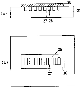
Figure 1(a) is a sectional schematic of one embodiment
of the diffraction grating-forming phase mask according to
the invention, and Figure 1(b) is a plan view thereof.
CA 02657509 2009-03-09
-10-
Figure 2 is a sectional schematic of another embodiment
of the diffraction grating-forming phase mask according to
the invention.
Figures 3(a) to 3(h) are sectional schematics
illustrating the process of fabricating the phase mask
according to the invention.
Figure 4(a) is a sectional schematic of one embodiment
of the diffraction grating-forming phase mask provided to
achieve the second object of the invention, and Figure 4(b)
is a plan view thereof.
Figures 5(a) to 5(h) are sectional schematics of the
process of fabricating Example 1 of the phase mask provided
to accomplish the second object of the invention.
Figures 6(a) to 6(e) are sectional schematics of the
process of fabricating Example 2 of the phase mask provided
to achieve the second object of the invention.
Figures 7(a) to 7(c) are illustrative of optical fiber
processing and a phase mask used therewith.
BEST MODE OF CARRYING OUT THE INVENTION
The diffraction grating-forming phase mask according to
the invention and the method thereof will now be explained
with reference to some preferred embodiments.
First of all, the diffraction grating-forming phase mask
provided to accomplish the first object of the invention is
explained with reference to its basic construction as well as
one embodiment of the fabrication method thereof.
Fig. 1(a) is a sectional schematic of one embodiment of
the diffraction grating-forming phase mask according to the
CA 02657509 2011-03-08
-11-
invention, and Fig. 1(b) is a plan view thereof. A phase
mask shown generally at 21 is a binary phase type diffraction
grating which, as is the Case` with a prior art phase mask,
comprises a substrate transparent tQ ultraviolet radiation,
e.g., a quartz glass substrate and an array of alternate
grooves 26 and strips 27 provided on one side of the
substrate at a given repetitive pitch and a given depth. In
the phase mask according to this embodiment, a sheet or film
form of protective layer 30 is provided over the side of the
substrate with the grooves 26 and strips 27 formed thereon,
thereby preventing entrance of foreign matters in grooves 26
or sublimation of an optical fiber-covering resin due to
ultraviolet radiation, which sublimation may otherwise cause
deposition of the resin to grooves 26. This protective layer
30, which is to be applied over the side of the phase mask 22
with the grooves 26 and strips 27 formed thereon, may be made
up of a sheet or film having a thickness of 0.1 mm to 2 mm
and comprising SiO2, CaF2, MgF2, ZrO, Hf0 or a fluorine resin
transparent to ultravia2,et radiation.
Here consider that the phase mask is irradiated at its
back side with ultraviolet laser light 23 while the side of
the phase mask with the grooves 26 and strips 27 formed
thereon is positioned in contact with an optical fiber 22
(Fig. 7) or spaced slightly away from the optical fiber 22.
Although resins, etc. are sublimated by ultraviolet radiation
from the covering 22B of the optical fiber 22, yet they are not
deposited into the grooves 26 because of being shielded by
the protective layer 30. This then enables a repetitive
CA 02657509 2009-03-09
-12-
pattern of the grating form of grooves 26 and strips 27 to be
so maintained that the diffraction grating formed on the
optical fiber 22 can be kept intact. The thus deposited
resins or other foreign matters can be easily wiped out of"
the surface of the protective layer 30.
Figs. 2(a) and 2(b) are sectional schematics of another
embodiment of the diffraction grating-forming phase mask
according to the invention. A phase mask shown generally at
21 is a binary phase type diffraction grating which, as is
the case with a prior art phase mask, comprises a substrate
transparent to ultraviolet radiation, e.g., a quartz glass
substrate and an array of alternate grooves 26 and strips 27
provided on one side of the substrate at a given repetitive
pitch and a given depth. In the phase mask according to this
embodiment as shown in Fig. 2(a), a material layer 31 made up
of CaF2, MgF2, ZrO, HfO or fluorine resin, which has a
refractive index deferment from that of the transparent
substrate and is transparent to ultraviolet radiation, is
formed on a surface of the phase mask with the grooves 26 and
strips 27 formed thereon by film formation techniques means
such evaporation, CVD, sputtering, and spin coating, thereby
filling at least the grooves 26 with the material 31. As
shown in Fig. 2(b), an exposed surface of the material layer
is then polished flat by polishing techniques such as CMP
(chemical mechanical polishing), so that the grooves 26 can
be filled up with the material 31 having a refractive index
different from that of the transparent substrate, thereby
making the surface of the phase mask flat. it is here to be
CA 02657509 2009-03-09
-13-
noted that polishing may be done in such a manner that a part
of the material layer 31 remains on the strips 27 or some
strips 27 become low.
In the phase mask according to this embodiment, too,
resins, etc. sublimated from the covering of an optical fiber
22 due to exposure to ultraviolet radiation are not deposited
into the grooves 26 because of being shielded by the.material
layer 31, as shown in Fig. 1. This then enables a repetitive
pattern of the grating form of grooves -26 and strips 27 to be
so maintained that the diffraction grating formed on the
optical fiber 22 can be kept intact. The thus deposited
resins or other foreign matters can be easily wiped out of
the flat surface of the phase mask.
It is to be understood that it is acceptable to form
such a protective layer 31 as shown in Fig. 1 on the phase
mask shown in Fig. 2(b).
Figs. 3(a) to Fig. 3(h) are sectional views of one
embodiment of the lithographic process of fabricating the
aforesaid phase mask 21. In these figures, reference numeral
10 represents a phase mask blank, 11 a quartz substrate, 12 a
chromium thin film, 12A a chromium thin-film pattern, 12B an.
opening in the chromium thin film, 13 an electron-beam
resist, 13A a resist pattern, 13B a resist opening, 14
electron beams, 21 a phase mask, 26 a groove, and 27 a strip.
As shown in Fig. 3(a), the blank 10 was first prepared
by forming the chromium thin film 12 of 150 A in thickness on
the quartz substrate 11. The chromium thin film 12 is useful
for preventing a charging-up of the electron-beam resist 13
CA 02657509 2009-03-09
-14-
at the electron-beam (14) irradiation step, and serves as a
mask in the formation of the groove 26 on the quartz
substrate. The thickness of'this chromium thin film is
important in view of resolution in chromium thin-film
etching,,and so should preferably be controlled to 100 to 200
A.
Then, electron-beam resist RE5100P (made by Hitachi
Kasei Co., Ltd.) as the electron-beam resist 13 was coated on
the chromium thin film 12 to a thickness of 400 nm, and
dried, as shown in Fig. 3(b).
After this, the electron-beam resist 13 was exposed to
light at an exposure of 1.2 pC/cm2, as shown in Fig. 3(c),
using an electron-beam writing system MEBESIII (made by
ETEC), so that portions corresponding to the grooves 26 were
exposed to the electron beams 14.
After the exposure, post-exposure baking (PEB) was
carried out at 90 C for 5 minutes, and the electron-beam
resist 13 was developed with TMAH (tetramethylammonium
hydroxide) at a concentration of 2.38%, thereby forming such
desired resist pattern 13A as shown in Fig. 3(d). It is here
noted that the post-exposure baking (PEB) is to selectively
enhance the sensitivity of the portions irradiated with the
electron beams 14.
Then, dry etching was performed with CH2C12 gas while the
resist pattern 13A was used as a mask, thereby forming such
chromium thin-film pattern 12A as shown in Fig. 3(e).
Subsequently, the quartz substrate 11 was etched with
CF4 gas to a depth of just 240 nm, while the chromium thin-
CA 02642430 2009-05-06
-15-
film pattern 12A was used as a mask, as shown Fig. 3(f).
Depth control was conducted by etching time control. Etching
can occur while the etching depth is controlled in the range
of 200 to 400 nm.
Following this, the resist pattern 13A was stripped off
with sulfuric acid at 70 C, as shown in Fig. 3(g). Finally,
the chromium thin-film pattern 12A was etched out with an
ammonium ceric nitrate solution, as shown in Fig. 3(h), and
scrubbing was carried out to obtain a complete line-and-space
phase mask 21 having a depth of 240 nm and a pitch of 1.070
pm, wherein the lines and spaces corresponded to strips 27
and grooves 26, respectively.
Finally, a synthetic quartz sheet of 0.5 mm in thickness
was applied on the thus prepared phase mask 21 to cover the
line-and-space pattern, so that such a complete phase mask as
depicted in Fig. 1 could be obtained.
The diffraction grating-forming phase mask provided to
accomplish the second object of the invention is now
explained with reference to its basic construction and one
embodiment of the fabrication method thereof.
Figs. 4(a) and 4(b) are sectional schematics of this
embodiment of the diffraction grating-forming phase mask
according to the invention. A phase mask shown generally at
1 comprises a quartz substrate 2 and a periodic groove 3
which is formed on its one side and is of a sine wave shape
in section. Theoretically, a grating having such a sectional
shape shows 0% transmittance with respect to zero-order
light, and causes. diffracted light to be primarily composed
CA 02657509 2009-03-09
-16-
of + first-order light and - first-order light. Therefore, a
diffraction grating fabricated into an optical waveguide such
as an optical fiber by means bf transfer using ultraviolet
laser light according to such an arrangement as depicted id
Fig. 7(a) can have so high performance that no noise can be
found in reflection spectra.
Such a groove 3 of a sine wave shape in section is
provided by forming a groove of a rectangular wave shape in
section on the quartz substrate 2, and-then etching the whole
surface of the side with the groove formed thereon for smooth
removal of the edges of the rectangular waves. For the
etching of the substrate having thereon the groove of a
rectangular wave shape in section, it is acceptable to make
use of drying etching. However, it is preferable to use wet
etching because of its high isotropy. Preferably in this
case, the wet etching should be carried out using an aqueous
alkali solution such as an aqueous sodium or potassium
hydroxide solution or a solution composed mainly of
hydrofluoric acid.
How to fabricate the phase mask 1 of the invention in an
optical fiber is explained with reference to examples.
Example 1
Fig. 5(a) to Fig. 5(h) are sectional views of one
embodiment of the process of fabricating the aforesaid phase
mask 1. In these figures, reference numeral 5 represents a
phase mask blank, 2 a quartz substrate, 4 a chromium thin
film, 4A a chromium thin-film pattern, 4B an opening in the
chromium thin film, 6 an electron-beam resist, 6A a resist
CA 02657509 2009-03-09
-17-
pattern, 6B a resist opening, 14 an electron beam, 1 a phase
mask, 3 a groove of a sine wave shape in section, 3' a groove
of a rectangular wave shape in section, 8 a strip of a sine
wave shape in section, and 8' a strip of a rectangular wave
shape in section.
As shown in Fig. 5(a), the blank 5 was first prepared by
forming the chromium thin film 4 of 20 nm in thickness on the
quartz substrate 2 by sputtering. The chromium thin film 4
is useful for preventing a charging-up of the electron-beam
resist 6 at the electron-beam (6) irradiation step, and
serves as a mask in the formation of the groove 3' on the
quartz substrate. The thickness of this chromium thin film
is important in view of resolution in chromium thin-film
etching, and so should preferably be controlled to 10 to 20
nm.
Then, electron-beam resist RE5100P (made by Hitachi
Kasei Co., Ltd.) as the electron-beam resist 6 was coated on
the chromium thin film to a thickness of 400 nm, and dried,
as shown in Fig. 5(b).
After this, the electron-beam resist 6 was exposed to
light at an exposure of 1.2 pC/cm2, as shown in Fig. 5(c),
using an electron-beam writing system MEBESIII (made by
ETEC), so that portions corresponding to the groove 3' were
exposed to the electron beams 7.
After the exposure, post-exposure baking (PEB) was
carried out at 90 C for 5 minutes, and the electron-beam
resist 6 was developed with TMAH (tetramethylammonium
hydroxide) at a concentration of 2.38%, thereby forming such
CA 02657509 2009-03-09
-18-
desired resist pattern 6A as shown in Fig. 5(d). It is here
noted that the post-exposure baking (PEB) is to selectively
enhance the sensitivity of the portion irradiated with the
electron beams 7.
Then, dry etching was performed with CH2C12 gas while the
resist pattern 6A was used as a mask, thereby forming such
chromium thin-film pattern 4A as shown in Fig. 5(e).
Subsequently, the quartz substrate 2 was etched with CF4
gas to a depth of just 240 nm, while the chromium thin-film
pattern 4A was used as a mask, as shown Fig. 5(f). Depth
control was conducted by etching time control. Etching can
occur while the etching depth is controlled in the range of
200 to 400 nm.
Following this, the resist pattern 6A was stripped off
with sulfuric acid at 70 C, whereupon the chromium thin-film
pattern 4A was etched out with an ammonium ceric nitrate
solution, and scrubbing was carried out to obtain a complete
line-and-space phase mask having a depth of 240 nm and a
pitch of 1.070 pm, wherein the lines and spaces corresponded
to strips 8' and grooves 3', respectively, as shown in Fig.
5(g)=
Subsequently, the Fig. 5(g) mask was wet etched at a
temperature 80 C using a 10% aqueous sodium hydroxide
solution, thereby obtaining a complete phase mask having a
diffraction grating pattern of such a sine wave shape in
section as depicted in Fig. 5(h).
Example 2
CA 02657509 2009-03-09
-19-
In this example, steps (a) to (b) are the same as those
shown in Figs. 5(a) to 5(d) for Example 1. That is, the
blank 5 was first prepared by' forming the chromium thin film
4 of 20 nm in thickness on the quartz substrate 2 by
sputtering, as shown in Fig. 5(a).
Then, electron-beam resist RE5100P (made by Hitachi
Kasei Co., Ltd.) as the electron-beam resist 6 was coated on
the chromium thin film to a thickness of 400 nm, and dried,
as shown in Fig. 5(b).
After this, the electron-beam resist 6 was exposed to
light at an exposure of 1.2 pC/cm2, as shown in Fig. 5(c),
using an electron-beam writing system MEBESIII (made by
ETEC), so that portions corresponding to the groove 3' were
exposed to the electron beams 7.
After the exposure, post-exposure baking (PEB) was
carried out at 90 C for 5 minutes, and the electron-beam
resist 6 was developed with TMAH (tetramethylammonium
hydroxide) at a concentration of 2.38%, thereby forming such
desired resist pattern 6A as shown in Fig. 5(d). It is here
noted that the post-exposure baking (PEB) is to selectively
enhance the sensitivity of the portion irradiated with the
electron beams 7.
Then, wet etching was carried out using the resist
pattern 6A as a mask, as shown in Fig. 6(a), thereby forming
such a chromium thin film 4A' as shown. 4B' represents an
opening in the chromium thin film.
CA 02657509 2009-03-09
-20-
Then, the quartz substrate was etched to a depth of just
240 nm using the resist pattern 6A as a mask with CF4 gas, as
shown in Fig. 6(c).
Then, while the remaining chromium thin film pattern 4A'
was used as a mask, wet etching was carried out with 5% HF,
as shown in Fig. 6(d). Following this, the chromium thin
film pattern 4A' was etched out with an ammonium ceric
nitrate solution. Finally, a complete phase mask 1 having a
diffraction grating pattern of such a sine wave shape as
shown in Fig. 6(e) was obtained through a scrubbing step.
Example 3
Using the method as already explained, a transparent
protective layer 30 was applied over the surface of the
transparent substrate (Fig. 1) fabricated according to the
Fig. 5 or 6 fabrication process. The section of the
repetitive groove (26)-and-strip (27) pattern shown in Fig. 1
was in a substantially sine wave shape, as can be seen from
the phase mask fabricated according to the Fig. 5 or 6
fabrication method. The transparent protective layer 30 was
applied with respect to this phase mask, thereby covering the
surface of the transparent substrate shown in Fig. 1.
Example 4
Using the method as already explained, a material layer
31, which has a refractive index different from that of the
transparent substrate of the phase mask fabricated according
to the Fig. 5 or 6 fabrication method and is transparent to
ultraviolet radiation, was applied over the substrate to fill
up the groove 3, followed by polishing. That is, the section
CA 02657509 2009-03-09
-21-
of the repetitive groove (26)-and-strip (27) pattern is in a
substantially sine wave shape, as can be seen from the phase
mask fabricated to the Fig. 5' or 6 fabrication method. The
transparent material 31 that has a refractive index different
from that of the transparent substrate shown in Fig. 2(a) and
transparent to ultraviolet radiation was applied over this
phase mask to fill up at least the groove 3. Following this,
the material layer 31 was polished, thereby obtaining such a
phase mask as shown in Fig. 2(b).
While the diffraction grating-forming phase mask of the
invention and its fabrication method have been described with
reference to some embodiments and examples, it is to be
understood that the invention is not specifically limited
thereto, and so many modifications may be made thereto.
INDUSTRIAL APPLICABILITY
In the phase mask embodiment provided to achieve the
object of the invention, the optically transparent protective
layer is applied over the surface of the substrate with the
repetitive groove-and-strip pattern formed thereon, or the
optically transparent material layer having a refractive
index different from that of the transparent substrate is
applied over the surface of the substrate by film-forming
means such as evaporation, CVD, sputtering or spin coating to
fill up at least the grooves while the portion of the
material layer exposed on the grooves is polished flat. Even
when foreign matters, resins sublimated from an optical
fiber, etc. are deposited on the surface of the phase mask,
therefore, the grating form of repetitive groove-and-strip
CA 02657509 2009-03-09
-22-
pattern per se is kept intact, so that no defect can be
introduced in the diffraction grating fabricated in the
optical fiber, etc. Such foreign matters, resins sublimated
from the optical fiber, etc. can be easily removed as by
wiping.
In the phase mask embodiment provided to accomplish the
second object of the invention, the section of the repetitive
groove-and-strip pattern is in a substantially sine wave
shape. When this diffraction grating-fabricating phase mask
is transferred into an optical waveguide such as an optical
fiber using ultraviolet laser light, it is thus possible to
fabricate a diffraction grating having so high performance
that no noise can be introduced in reflection spectra.
According to the fabrication method of the invention
wherein a grating form of groove of a rectangular shape in
section is periodically provided on one side of the
transparent substrate, and wet etching is then carried out
using an aqueous alkali solution or a hydrofluoric acid
solution or its buffer solution to convert the sectional
shape into a substantially sine wave shape, it is possible to
make a diffraction grating-fabricating phase mask with the
addition of simple steps.
The first and second objects of the invention may be
achieved at the same time.