Note : Les descriptions sont présentées dans la langue officielle dans laquelle elles ont été soumises.
CA 02657783 2009-01-13
1
DESCRIPTION
HIGH-PRESSURE DISCHARGE LAMP LIGHTING DEVICE
AND
LIGHTING FIXTURE USING THE SAME
Technical Field
[0001]
This invention relates to a high-pressure discharge lamp lighting device and
a lighting fixture using the same.
Background Art
[0002]
A high-pressure discharge lamp tends to suffer from unstable discharge
immediately after it is triggered or when it comes close to the end of its
lifetime. It is well known that the discharge lamp may blink, or fade out in
the worst case even if a lighting device supplies power.
[0003]
As shown in Fig. 21 of the accompanying drawing figures, rectification
discharge is known as one of causes of the foregoing problems. With the
rectification discharge, emission of electrons between a pair of electrodes of
an AC-activated discharge lamp becomes asymmetric in anodic and cathodic
cycles. This is caused by unreliable formation of so-called luminescent
spots, i.e. unstable discharge of thermal electrons, since one electrode in
the
cathodic cycle cannot shift to arc discharge from glow discharge. Such a
phenomenon is somewhat inevitable to the discharge lamp. In the case
shown in Fig. 21, it is known that an electrode 1 cannot sufficiently
discharge
electrons in the cathodic cycle.
[0004]
It is conceivable that the unstable state of the luminescent spots of the
CA 02657783 2009-01-13
2
electrodes are triggered because the electrodes or radioactive substances in
electrons are exhausted, or because discharging functions of the discharge
lamp become unstable due to impurities.
[0005]
In any case, the discharge lamp suffers from increased impedance, and
blinks or fades out due to insufficient power of the lighting device if no
countermeasures are taken.
[0006]
Ftiirther, there is a phenomenon in which the discharge lamp is turned on
once, and transiently and abruptly increases its impedance. Especially, this
phenomenon is remarkable with a so-called metal halide lamp in which a
metal halogen compound is sealed in a discharge tube of the discharge lamp
as a light-emitting substance. Specifically, the phenomenon is observed
when the discharge lamp is in a startup mode and when it is in a steadily
lighting mode.
[0007]
The foregoing phenomena will be described with respect to behavior of the
metal halide lamp. In the startup mode, the lamp is triggered by
simultaneous dielectric breakdown of the light emitting substances and a
combination of inert gases and mercury vapors, both of which are sealed in a
discharge tube. In this state, the metal halogen compound has a low vapor
pressure, and hardly contributes to discharge.
[0008]
Thereafter, electric power is applied to the discharge tube for several
minutes.
When the discharge tube becomes hot, the light emitting substance becomes
loose, the vapor pressure of the metal is raised, and a lamp voltage is
increased.
[0009]
What is unexpected in the foregoing process is that the vapor pressure of the
metal is raised instantly and abruptly if the light emitting substance is
CA 02657783 2009-01-13
3
present at an unstable spot, e.g. near a hot electrode, and comes into contact
with the hot electrode. In such a case, if a magnetic ballast whose power
supply performance depends upon the commercial power supply, a voltage of
the lamp exceeds an output of the ballast, so that the lamp fades out. A
similar phenomenon is observable when the commercial power supply is
interrupted in a split second and when the commercial power supply voltage
is instantly decreased.
[0010]
On the other hand, an electronic ballast includes a so-called inverter circuit
which lights the lamp with the rectangular wave AC, and controls lamp
power to be approximately constant. If the lamp voltage varies as stated
above, a lamp current is reduced. As a result, the lamp impedance is
transiently raised, which makes the lamp fade out. Referring to Fig. 22, the
lamp voltage is abruptly raised from a value at an operation point 1 to a
value at an operation point 2.
[0011]
Further, there is another reason for the increase of the lamp voltage. For
instance, even a good lamp may suffer from an increased voltage with a lapse
of time. This is caused by chemical reactions of the substance sealed in the
lamp, or release of impurities. This phenomenon is essentially inevitable,
and leads to the foregoing phenomena.
[0012]
The following describe behavior of the ballast. With the ballast used for an
AC-powered discharge lamp, a lamp current is turned off once each time
polarity reversal is performed in a half cycle. In order to restart the lamp
in
a next half cycle, the lamp voltage from the ballast is supplied first while
the
lamp current which is emission of thermal electrons of the electrodes is
supplied after a while. Therefore, impedance is transiently increased as
shown by a white circle. The white circle denotes a transient value of the
high impedance in the half cycle.
CA 02657783 2009-01-13
4
[0013]
When the lamp is activated by the commercial power having sine waves with
delayed rising edges, the lamp voltage becomes a so-called re-striking voltage
which is abruptly raised after the zero-cross. This makes the lamp fade out
when the power supply voltage becomes insufficient.
[0014]
On the other hand, with a rectangular wave inverter circuit whose waveform
quickly rises, an output voltage can be advantageously controlled to be
constant. However, when the lamp voltage is also controlled to be
approximately constant, the lamp current is decreased in spite of the
increase of the lamp voltage. Referring to Fig. 24, the lamp impedance is
transiently raised, which causes the lamp to fade out. In Fig. 24, the lamp is
operated at an operation point 2' where the lamp voltage is increased when
an ideal power source (a constant voltage source, for example) is used.
However, the impedance is raised to the value at the operation point 2 along
an output line of the constant power supply.
[0015]
Japanese Patent Laid-Open Publication No. Sho 60-250599 discloses a
discharge lamp lighting device, which includes a DC-DC converter having
current limiting characteristics, and a rectangular wave inverter converting
an output of the DC-DC converter into a rectangular wave AC. The
discharge lamp lighting device supplies the output of the rectangular wave
inverter to the discharge lamp via a high voltage pulse superimposing circuit.
The discharge lamp lighting device controls current limiting characteristics
in
response to detected output values of the DC-DC converter, output current
and discharge tube voltage. However, the lighting device does not control
the current flowing to switching elements to a predetermined peak value in
each switching cycle when the discharge lamp tends to fade out.
[0016]
In summary, the phenomena which cause unstable lighting and fading out of
CA 02657783 2009-01-13
the discharge lamp are not favorable to the discharge lamp and the ballast
for the following reasons.
[0017]
(1) The lamp asymmetrically discharges.
5 [0018]
(2) The lamp increases the impedance due to the transient behavior or aging.
[0019]
(3) The ballast does not have a sufficient output (or power supply
performance).
[0020]
An electric model of the discharge lamp will be reviewed hereinafter.
[0021]
Fig. 25 is a graph showing voltage-current characteristics of the discharge
lamp from its startup mode till its steadily lighting mode. For convenience
sake, the voltage-current characteristics per half cycle are depicted.
[0022]
At an operation point (a), the discharge lamp undergoes voltage breakdown
by high voltage pulses coming from outside. In this state, the discharge
lamp remains in a transient state between the glow discharge and the arc
discharge, and has high impedance.
[0023]
When an appropriate ballast output is supplied, the lamp changes to a mode
shown at an operation point (b) where the lamp is quasi-stable. In this state,
the discharge lamp has undergone current breakdown, but maintains a high
lamp voltage, and has impedance which is not lowered completely.
[0024]
Next, when a ballast output which can apply an approximately rated current,
the lamp completely changes its state to a state shown at to an operation
point (c) where the impedance and a voltage are low, and a lamp current is
large.
CA 02657783 2009-01-13
6
[0025]
Thereafter, the lamp voltage gradually increases as shown by an output
curve of the ballast. The lamp becomes stable at a rated operation point (d)
along with an increase of the impedance.
[0026]
When the lamp is new, it becomes stable at the operation point (d) each time
it is lit. With a lapse of time, the lamp gradually increases its voltage as
shown at operation points (d) -* (d") -> (d").
[0027]
In Fig. 26, the lamp voltage is in a normal range at the operation points (d')
to
(d") while it is abnormal at the operation point (d").
[0028]
The lamp impedance is variable as shown by dashed lines.
[0029]
Further, the lamp is assumed to be in operation with a constant current
between the operation points (c) and (d"').
[0030]
In order to overcome the foregoing problems, it is necessary to apply
optimum ballast outputs at the respective operation points (a) ---+ (b) -+ (c)
(d) --). (d) -> (d") , (d").
[0031]
The present invention has been contemplated in order to overcome problems
of the related art, and is intended to provide a high-pressure discharge lamp
lighting device which can protect a discharge lamp against unstable lighting
and fading out from the startup till the end of life.
Disclosure of Invention
[0032]
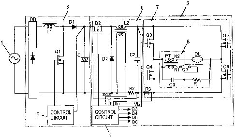
Referring to Fig. 1, a high voltage discharge lamp lighting device includes: a
power converter circuit 3 which includes a plurality of switching elements Q2
CA 02657783 2009-01-13
7
to Q6 and an inductance element L2, converts an input from a DC power
supply 2, and supplies a rectangular wave AC output to a high-pressure
discharge lamp DL; and a control circuit 9 which controls the switching
elements Q2 to Q6 of the power converter circuit 3. The control circuit 9
performs first lighting control in which the switching elements Q2 to Q6 of
the power converter circuit 3 are controlled in order to supply a current to a
peak value for each switching cycle, and performs second lighting control in
which desired power is supplied during steadily lighting state of the
high-pressure discharge lamp DL; and the first lighting control and the
second lighting control are switched over in response to a lighting state of
the
high-pressure discharge lamp DL.
Brief Description of the Drawings
[0033]
[Fig. 1]
Fig. 1 is a circuit diagram of a discharge lamp lighting device in a first
embodiment of the invention.
[Fig. 2]
Fig. 2 is a diagram showing a process from a no load mode till a steadily
lighting mode in the first embodiment of the invention.
[Fig. 3]
Fig. 3 shows waveforms of respective circuits during constant current
control.
[Fig. 4]
Fig. 4 is a chart showing variations of a lamp voltage from dielectric
breakdown till a steadily light mode, and a control switching point in the
first
embodiment of the invention.
[Fig. 5]
Fig. 5 is a characteristic diagram showing lamp power with respect to a lamp
voltage, and a target control value of a lamp current.
CA 02657783 2009-01-13
8
[Fig. 6]
Fig. 6 explains behavior of the lamp voltage and the lamp current for each
polarity reversal in the first embodiment.
[Fig. 7]
Fig. 7 is a circuit diagram of a discharge lamp lighting device in a second
embodiment.
[Fig. 8]
Fig. 8 shows waveforms of respective circuits during the constant current
control.
[Fig. 9]
Fig. 9 is a chart showing variations of a lamp voltage from the dielectric
breakdown till the steadily lighting mode, and a control switching point in
the
second embodiment of the invention.
[Fig. 10]
Fig. 10 is a circuit diagram of a discharge lamp lighting device according to
a
third embodiment.
[Fig. 111
Fig. 11 is a diagram showing processes from the no load mode till the steadily
lighting mode in the third embodiment of the invention.
[Fig. 12]
Fig. 12 shows waveforms of respective circuits during the constant current
control.
[Fig. 13]
Fig. 13 is a chart showing variations of a lamp voltage from the dielectric
breakdown till the steadily lighting mode, and a control switching point in a
third embodiment of the invention.
[Fig. 14]
Fig. 14 shows waveforms of respective circuits during the constant current
control in a fourth embodiment.
[Fig. 15]
CA 02657783 2009-01-13
9
Fig. 15 is a chart showing variations of a lamp voltage from the dielectric
breakdown till the steadily lighting mode, and a control switching point in a
fifth embodiment of the invention.
[Fig. 16]
Fig. 16 is a chart showing variations of a lamp voltage from the dielectric
breakdown till the steadily lighting mode, and a control switching point in a
sixth embodiment of the invention.
[Fig. 17]
Fig. 17 shows waveforms of respective circuits during a constant current
control mode in a sixth embodiment.
[Fig. 18]
Fig. 18 is a chart showing variations of a lamp voltage from the dielectric
breakdown till the steadily light mode, and a control switching point in a
seventh embodiment of the invention.
[Fig.19]
Fig. 19 is a characteristic diagram showing lamp power with respect to a
lamp voltage, and a target control value of a lamp current.
[Fig. 20]
Fig. 20 shows external appearances of lighting fixtures in a ninth
embodiment of the invention.
[Fig. 21 ]
Fig. 21 shows waveforms of rectifying discharge currents of a high-pressure
discharge lamp of the related art.
[Fig. 22]
Fig. 22 shows transient line impedance characteristic 1 of the related art.
[Fig. 23]
Fig. 23 shows transient line impedance characteristic 2 of the related art.
[Fig. 24]
Fig. 24 shows transient line impedance characteristic 3 of the related art.
[Fig. 25]
CA 02657783 2009-01-13
Fig. 25 shows line impedance characteristics at the time of startup, during a
steadily lighting mode, and at the end of life of a discharge lamp in the
related art.
[Fig. 26]
5 Fig. 26 is a chart explaining output characteristics of a ballast of the
related
art.
[Fig. 27]
Fig. 2 is a further chart explaining output characteristics of a ballast of
the
related art.
10 [Fig. 28]
Fig. 28 shows the relationship between a rated lamp operation current and a
minimum initial operation current of the related art.
[Fig. 29]
Fig. 29 is a chart explaining output characteristics of a ballast of the
related
art.
Best Mode for Carrying Out the Invention
[0034]
The invention will be described hereinafter on the basis of the concept of the
operation points of the discharge lamp referred to above. Usually, a
discharge lamp suffers from unstable lighting and fading out due to the three
problems described above. The inventors of the invention have discovered
that the problems can be solved by actively controlling output characteristics
of the ballast.
[0035]
For instance, refemng to the output characteristics shown in Fig. 26, the
stable operation point (b) is lowered to the low current point (b), or there
is
no intersection in response to a slight change of the lamp impedance. As a
result, the lamp will fade out. In Fig. 26, the output characteristics of the
ballast are depicted as voltage - current characteristics linldng an open
CA 02657783 2009-01-13
11
voltage V02 and a short-circuit current Is.
[0036]
Taking unpredictable behavior of the lamp into consideration, it is preferable
that the state of the lamp at the operation point (b) should be stabilized
based on the output characteristics of the ballast. Specifically, it is
preferable that the operation point (b) should be moved to the operation point
(b") shown in Fig. 27, for instance, so that an intersection is present in a
more stable operation region.
[0037]
The inventors have tested that a minimum current required at the operation
point (b) may be equal to or larger than 600mA (refer to Fig. 28). In Fig. 28,
white circles denote a variety of lamps, the abscissa denotes a rated
operating
current, and the ordinate denotes a minimum current (mA) necessary for
triggering the lamps.
[0038]
If the power is controlled to be constant in a mode between the operation
point (b) and the operation point (c), a lamp which has changed its glow
discharge to the arc discharge becomes unstable again. In this state, it is
necessary to let the lamp have low impedance.
[0039]
When the lamp is confirmed to be out of the unstable state between the
operation point (c) and the operation point (d"), constant current or power
control may be performed as shown by a characteristic curve B in Fig. 29.
Specifically, the current is controlled to be constant in the mode between the
operation point (c) and the operation point (d) while the power is controlled
to
be constant between the operation point (d) and the operation point (d").
[0040]
Finally, between the operation point (d") and the operation point (d"j or the
fmal life stage, the lamp increases its impedance. In this state, it is not
preferable to apply unnecessary power to the lamp, which may damage or
CA 02657783 2009-01-13
12
overheat the discharge lamp or the ballast. Therefore, it is effective to cut
off
an output which has a voltage above the constant voltage as shown by a
characteristic curve C in Fig. 29 or not to apply the power above the
predetermined value, so that the lamp will naturally fade out.
[00411
Specific embodiments for canying out the foregoing operations will be
described hereinafter.
[0042]
(FIRST EMBODIMENT)
Fig. 1 is a circuit diagram of a discharge lamp lighting device in a first
embodiment of the invention. In Fig. 1, reference numeral 1 denotes an AC
power supply, reference numeral 2 denotes a DC power supply circuit, and
reference numeral 3 denotes a power converter circuit. The DC power
supply circuit 2 includes: a rectifier DB for full-wave rectification of the
AC
power source 1; a booster chopper circuit which is constituted by an inductor
L 1, a switching element Q 1, a diode D 1 and a capacitor C 1; and a control
circuit 5 for the booster chopper circuit. An AC input from the AC power
source 1 is converted into a DC output, which is supplied to the power
converter circuit 3. Further, the control circuit 5 performs power factor
improvement control for the circuits of the lighting device so that the
lighting
circuit becomes more resistive and so that the input current and the input
voltage do not suffer from a phase lag. For instance, the control circuit 5
for
the switching element Q 1 may be realized by a commercially available
MC33262 manufactured by on-semi Co., Ltd.
[0043]
The power converter circuit 3 includes a step-down chopper circuit 6, an
inverter circuit 7, an igniter circuit 8, and a control circuit 9. The step-
down
chopper circuit 6 includes a switching element Q2, a diode D2, an inductor
L2, and a capacitor C2. The step-down chopper circuit 6 reduces an input
voltage, and outputs a DC voltage. The operation of the step-down chopper
CA 02657783 2009-01-13
13
circuit 6 is well-known, and will not be described here. The step-down
chopper circuit 6 controls the operation of the switching element Q2, and
serves as a ballast which controls power supplied to a discharge lamp DL.
[0044]
The inverter circuit 7 is a full-bridge circuit constituted by switching
elements Q3 to Q6. In the inverter circuit 7, a pair of switching elements Q3
and Q6 and a pair of switching element Q4 and Q5 are alternately turned on
and off in response to control signals from the control circuit 9 at several
ten
to several hundred Hertz frequency, so that rectangular wave AC power is
supplied to the discharge lamp DL.
[0045]
The igniter circuit 8 includes a pulse transformer PT, a capacitor C3, a
switching element Q7 (e.g. a voltage responsive element such as SIDAC, and
a resistor R1. The operation of the igniter circuit 8 will be briefly
described
hereinafter. Receiving the rectangular wave voltage generated by the
inverter circuit 7, the capacitor C3 is gradually charged in accordance with
its time constant and a time constant of the resistor R 1. When a voltage Vc3
of the capacitor C3 becomes equal to a break-over voltage Vbo in a no load
period, the switching element Q7 is activated. Charges accumulated in the
capacitor C3 are discharged via the switching element Q7, and a primary coil
N 1 of the pulse transformer PT. A pulse voltage generated in the primary
coil N 1 of the pulse transformer PT is raised, so that a high pulse voltage
(of
several KV) is generated in a secondary coil N2 of the pulse transformer PT.
In this state, the discharge lamp DL starts discharging in response to the
high pulse voltage, and changes its state to a lighting mode.
[0046]
The control circuit 9 detects a lamp voltage Vla of the discharge lamp DL, a
lamp current Ila, a peak current Ip of the switching element Q2, and a
zero-cross signal (ZCS) of a current flowing to the inductor L2. The control
circuit 9 turns on or off the switching element Q2 on the basis of the
detected
CA 02657783 2009-01-13
14
results, and controls the operation of the switching element Q2 of the
step-down chopper circuit 6 and the switching elements Q3 to Q6 of the
inverter circuit 7, so that a desired current or power is supplied to the
discharge lamp DL.
[0047]
The discharge lamp DL is a high intensity-and-voltage discharge lamp (HID
lamp) such as a metal halide lamp and a high-voltage mercury lamp.
[0048]
Using the control circuit 9, the lighting device goes through roughly three
modes as shown in Fig. 2 while the control circuit 9 controls the unlit mode
of the discharge lamp, and puts the discharge lamp in a steady lighting
mode.
[0049]
No load mode: The discharge lamp remains unlit. The pulse voltage
generated by the igniter circuit 8 is boosted to the primary and secondary
coils N 1 and N2 of the pulse transformer PT, is superimposed on a
rectangular wave voltage, and is applied between electrodes of the discharge
lamp. In this state, the discharge lamp undergoes dielectric breakdown, and
is put in a startup mode.
[0050]
Startup Mode: After the dielectric breakdown, the discharge lamp starts arc
discharge via glow discharge. The lamp voltage of several volts is gradually
raised to a stable voltage in several minutes.
[0051]
Steadily Lighting Mode: A temperature of the discharge tube is raised in
several minutes after the discharge lamp is lit. The discharge lamp becomes
steady, and the lamp voltage becomes approximately constant.
[0052]
Fig. 3 shows operating waveforms of various circuits during the startup mode
or the steadily lighting mode of the discharge lamp. The step-down chopper
CA 02657783 2009-01-13
circuit 6 turns the switching element Q2 on and off in response to a PWM
signal from the control circuit 9. In response to chopping of the switching
element Q2, the step-down chopper circuit 6 generates a chopping wave IL2
as shown in Fig. 3, and provides a load circuit with a rectangular current Ila
5 which has been smoothed by the capacitor C2. The chopping wave IL2 flows
to the inductor L2, and gradually increases while the switching element Q2 is
active, but gradually decreases while the switching element Q2 is inactive.
[0053]
In the inverter circuit 7, the pair of switching elements Q3 and Q6 and the
10 pair of switching elements Q4 and Q5 are alternately turned on in response
to the control signals from the control circuit 9, so that the rectangular
wave
current Ila (shown in Fig. 3) is supplied to the discharge lamp DL, and a
voltage Vla (shown in Fig. 3) is supplied to the opposite ends of the
discharge
lamp. Polarity reversal is carried out in a similar manner from the no load
15 mode till the steady lighting mode. Alternatively, polarity reversal may be
performed in a different manner during the no load mode and during the
steadily lighting mode.
[0054]
The control processes from the dielectric breakdown till the steadily lighting
mode of the discharge lamp will be described in detail with reference to Fig.
4,
in which the abscissa denotes a time axis.
[0055]
Constant Current Control
Lamp power Wla, which is calculated using detected values of the lamp
voltage Vla and lamp current Ila, is detected as a light discriminating point
A.
In this state, the discharge lamp is judged to be lit. From this time point, a
peak of the current is controlled to be constant in order that a current
having
a magnitude Tip, which is a target value of a current curve shown in Fig. 5,
is
made to flow in each switching cycle of the switching element Q2.
[0056]
CA 02657783 2009-01-13
16
To be more precise, when the switching element Q2 is turned on in response
to a command from the control circuit 9, a current begins to flow to the
inductor L2. The switching element Q2 is turned off when a current value Ip
of the switching element Q2 which is detected by the current sensing resistor
R2 becomes equal to the target value Tip (shown in Fig. 5). When the
zero-cross signal ZCS is detected to be zero by the secondary coil of the
inductor L2, the control circuit 9 outputs the signal to activate the
switching
element Q2. Thereafter, the foregoing operation will be repeated.
[0057]
Fig. 6 shows the relationship between the voltage Vla and the current Ila of
the discharge lamp each time the polarity reversal is carried out. Referring
to Fig. 3 and Fig. 6 in combination, it is known that when the substance
sealed in the discharge lamp is unstable in the startup mode, a voltage VX is
high, and the current Ila is slow to flow immediately after the polarity
reversal.
[0058]
Even immediately after the polarity reversal where the current is slow to
flow,
constant current control makes the current flow to the peak value, which can
prevent the discharge lamp from fading out.
[0059]
Constant Power Control
When the lamp voltage is raised to become equal to a predetermined voltage
Vla l(shown in Fig. 4), the constant current control is switched over to
constant power control which is second control. In this power control mode,
chopping of the switching element Q2 is controlled on the basis of a Vla -
Twla curve shown in Fig. 5 each time the lamp voltage Vla is detected while
the discharge lamp is active.
[0060]
In the first embodiment, it is possible to reliably apply the necessary
current
even when the substance sealed in the discharge lamp is unstable at the
CA 02657783 2009-01-13
17
startup of the discharge lamp, and especially even when the lamp impedance
is increased immediately after the polarity reversal, and the current is slow
to
flow to the discharge lamp. Therefore, the discharge lamp can be reliably lit
in response to each polarity reversal. Further, this embodiment can realize
the high-pressure discharge lighting device in which the output voltage of the
booster chopper circuit is reduced in order to make components have low
withstand voltages.
[00611
(SECOND EMBODIMENT)
Fig. 7 is a circuit diagram of a lighting device according to a second
embodiment of the invention. In this embodiment, a half-bridge inverter
circuit is used as the power convertor circuit 3. The half-bridge inverter
circuit includes the following components: a series circuit of electrolytic
capacitors C 1 and C2, and a series circuit of the switching elements Q2 and
Q3 which are connected to the an output of the DC power supply circuit 2 in
parallel; a series circuit of the inductor L2 and capacitor C4 which is
connected between contacts of the capacitors Cl and C2 and contacts of the
switching elements Q2 and Q3 via the current sensing resistor R2; and the
discharge lamp DL is connected in parallel with the capacitor C4 via the
secondary coil N2 of the pulse transformer PT. The half-bridge inverter
functions both as the step-down chopper circuit 6 and the inverter 7. The
series circuit of the inductor L2 and the capacitor C4 constitutes a low-pass
filter circuit for the step-down chopper circuit. A low frequency rectangular
wave voltage is produced at opposite ends of the capacitor C4 when a period
T1 and a period T2 alternate at low frequencies of several ten to several
hundred Hertz frequency. In the period Tl, the switching element Q2 is
turned on and off at high frequencies of several ten to several hundred kHz in
response to the control signal from the control circuit 9. In the period T2,
the switching element Q3 is turned on and off at high frequencies of several
ten to several hundred kHz in response to the control signal from the control
CA 02657783 2009-01-13
18
circuit 9.
[0062]
The control circuit 9 detects the lamp voltage Vla using a lamp voltage
detecting circuit 11, and detects an instant value Ip of the current flowing
through the switching elements Q2 and Q3 by means of the chopper current
detecting circuit 12. Further, the control circuit 9 detects the zero-cross
signal (ZCS) flowing through the inductor L2 by means of the zero-cross
signal detecting circuit 13. The control circuit 9 controls the switching
elements Q2 and Q3 in response to the detected results. The igniter circuit
8 is configured similarly to that employed in the first embodiment. However,
in this embodiment, the igniter circuit 8 is connected to the output of the DC
power supply circuit via the switching element Q8 whose operation is
controlled in response to the control signal from the control circuit 9.
[0063]
In this embodiment, the lighting device undergoes the no load mode, startup
mode and steadily lighting mode as shown in Fig. 2 from the unstable mode
till the steadily lighting mode of the discharge lamp.
[0064]
Fig. 9 shows the foregoing three modes of the discharge lamp from the
dielectric breakdown till the steadily lighting. The abscissa denotes a time
axis.
[0065]
Constant Current Control
After the dielectric breakdown of the discharge lamp, the control circuit 9
detects a decrease of the lamp voltage Vla. The discharge lamp is judged to
be lit when the point A, where the lamp voltage Vla is equal to or lower than
the predetermined threshold value, is detected. The point A is used to judge
whether or not the discharge lamp is lit. In this state, a peak of the current
is controlled to be constant so that the current having the target amount Tip
is reliably applied to the switching element Q2 (or Q3) in each switching
cycle.
CA 02657783 2009-01-13
19
Refer to Fig. 5. This operation is shown in Fig. 8.
[0066]
In the period Tl, the switching element Q2 is turned on in response to a
command from the control circuit 9, and the current begins to flow through
the inductor L2. When the chopper current Ip from the current sensing
resistor R2 becomes equal to the target current value Tip detected by the
chopper current sensing circuit 12, the switching element Q2 is turned off.
Thereafter, when the zero-cross signal ZCS is detected to be zero by the
secondary coil of the inductor L2, the control circuit 9 issues a signal to
activate the switching element Q2. The foregoing operations will be repeated
hereinafter.
[0067]
During the period T2, the switching element Q3 is turned on in response to
the command from the control circuit 9, so that the current flows through
the inductor L2 in the opposite direction. When the chopper current Ip from
the current sensing resistor R2 is detected to be equal to the target current
value TIp, the switching element Q2 is turned off. Thereafter, when the
zero-cross signal ZCS is detected to be zero by the secondary coil of the
inductor L2, a signal is issued in order to turn the switching element Q2 on.
The foregoing operations are repeated.
[0068]
The high frequency switching operations in the periods T1 and T2 are
alternately carried out at the low frequency. The rectangular wave lamp
voltage Vla is applied to the opposite ends of the discharge lamp as shown in
Fig. 8, so that the rectangular wave lamp current Ila flows.
[0069]
Constant Power Control
When a predetermined period t 1 elapses after the discharge lamp is lit, the
control is switched over from the constant current control to constant power
control, which is second control. In order to stabilize the discharge lamp
CA 02657783 2009-01-13
with desired power within the rated lighting voltage, the switching elements
Q2 and Q3 is turned on with the predetermined ON period according to the
detected Vla.
[0070]
5 In the second embodiment, the state of the gas sealed in the discharge lamp
is unstable in the startup mode, and the current does not smoothly flow to
the discharge lamp because the lamp impedance is increased immediately
after the polarity reversal. However, the present invention can provide the
high-pressure discharge lamp lighting device, in which the necessary current
10 can flow in this state, the discharge lamp can be reliably lit each time
the
polarity reversal is carried out, the output voltage of the booster chopper
circuit 2a is set to be low, and withstand voltage of the components can be
lowered.
[0071]
15 (THIRD EMBODIMENT)
Fig. 10 is a circuit diagram of a lighting device according to a third
embodiment of the invention. In this embodiment, a full-bridge inverter
circuit 7 is used as the power converter circuit, and also functions as the
booster chopper circuit 6 and the igniter circuit 8 by artfully controlling
the
20 switching elements Q3 to Q6. Specifically, the switching elements Q3 and
Q4 are turned on and off at the high frequency in the no load mode, which
enables a resonant booster circuit 8 to generate a high voltage and
dielectrically breaks down the discharge lamp DL. The resonant booster
circuit 8 is constituted by a transformer PT and a capacitor C3 inserted
across an intermediate tap of the transformer Pt and the earth. From the
startup mode till the steadily lighting mode of the discharge lamp, the
switching elements Q3 and Q4 are turned on and off at the low frequency,
which enables the resonant booster circuit 8 to stop generating the high
voltage. During the period Tl where the switching element Q4 is active, the
switching elements Q5 and Q6 are alternately is turned on and oflff.
CA 02657783 2009-01-13
21
Specifically, the switching element Q5 is tu.rned on and off at the high
frequency while the switching element Q6 is turned on and off at the low
frequency. The low frequency rectangular wave voltage is supplied to the
discharge lamp DL. In this state, the inductor L2 and the capacitor C2
function as a low-pass filter for the booster chopper circuit.
[0072]
The control circuit 9 detects the lamp voltage Vla on the basis of the
voltages
Vla 1 and V1a2 at the opposite ends of the discharge lamp, and the instant
value Ip of the chopper current flowing to the switching elements Q5 and Q6
from the current sensing resistor R2. Further, the control circuit 9 detects
the zero-cross signal ZCS in the current flowing to the inductor L2. Still
further, the control circuit 9 controls the switching elements Q3 to Q6 in
order to supply the desired current or voltage to the discharge lamp on the
basis of the detected results.
[0073]
Referring to Fig. 11, the control circuit 91ets the lighting device undergo
three
modes from the unlit state till the steadily lighting mode of the high voltage
discharge lamp.
[0074]
No load mode: The discharge lamp remains unlit. A resonant pulse voltage,
which is generated by turning on and off the switching elements Q3 and Q4
approximately at an LC resonant frequency of the primary coil of the
transformer PT and the capacitor C3, is boosted on the basis of a turn ratio
of the transformer PT, and is supplied across the electrodes of the discharge
lamp. The discharge lamp undergoes the dielectric breakdown, and is put
in the startup mode.
[0075]
[Startup Mode]
After the dielectric breakdown, the discharge lamp undergoes shifts to the arc
discharge from the glow discharge. While the discharge lamp becomes
CA 02657783 2009-01-13
22
stable after the arc discharge is started and a temperature inside the
discharge tube becomes uniform, the lamp voltage of several volts is
gradually raised to the stable voltage in several minutes.
[0076]
Steadily lighting Mode: After the discharge lamp is lit, the temperature
inside
the discharge tube is raised in several minutes. The discharge lamp
becomes stable, and the lamp voltage becomes approximately constant.
[0077]
Fig. 12 shows waveforms of various circuits in the startup mode or the
steadily lighting mode. The control circuit 9 controls the switching elements
Q3 to Q6 in the inverter circuit 7 as described hereinafter. The periods T1
and T2 alternate at low frequencies of several ten to several hundreds Hz.
During the period Tl, the switching element Q5 is turned on and off at the
frequencies of several ten to several hundreds kHz while the switching
element Q4 remains active. During the period T2, the switching element Q6
is turned on and off at the frequencies of several ten to several hundreds kHz
while the switching element Q3 remains active. A chopping wave Ir.2 is
generated in response to the chopping of the switching elements Q5 and Q5
as shown in Fig. 12. The current Ila smoothed by the capacitor C2 is
applied to the load circuit. The chopping wave II2 2 is a current flowing to
the
inductor L2, and gradually increases while the switching element Q2 is active,
and gradually decreases while the switching element Q2 is inactive.
[0078]
The modes from the dielectric breakdown till the steadily lighting mode of the
discharge lamp will be described in detail with reference to Fig. 13. In Fig.
13, the abscissa denotes the time axis.
[0079]
Constant Current Control
After the dielectric breakdown of the discharge lamp, an increase of the lamp
current Ila is detected. When detecting the lighting judging point A where
CA 02657783 2009-01-13
23
the increased lamp current is equal to or larger than the threshold Ilal, the
discharge lamp is judged to be lit. From this time point, the peak of the
increased lamp current is controlled to be constant so that the current
having the target amount TIp reliably flows during each chopping period of
the switching element Q5 or Q6. Refer to Fig. 5 with respect to the target
amount Tip in the current curve.
[0080]
The switching element Q4 is kept active during the period Tl while the
switching element Q5 is controlled as follows. The switching element Q5 is
turned on in response to the command from the control circuit 9, and the
current begins to flow to the inductor L2. When the chopper current Ip
detected by the current sensing resistor R2 becomes equal to the target
current value Tlp (shown in Fig. 5), the switching element Q5 is turned off.
The zero-cross signal ZCS is detected based on a potential at an intersection
of the switching elements Q5 and Q6, so that the control circuit 9 issues the
signal to turn on the switching element Q5. The foregoing operations will be
repeated.
[0081]
During the period T2, the switching element Q3 is kept active while the
switching element Q6 is controlled as follows. The switching element Q6 is
turned on in response to the command from the control circuit 9, and the
current begins to flow to the inductor L2. When the chopper current Ip from
the current sensing resistor R2 is detected to be equal to the target current
value Tip (shown in Fig. 5), the switching element Q6 is turned off. The
zero-cross signal ZCS is detected based on a potential at an intersection of
the switching elements Q5 and Q6, so that the control circuit 9 issues the
signal to turn on the switching element Q6. The foregoing operations will be
repeated.
[0082]
The periods Tl and T2 alternate at the low frequencies. The rectangular
CA 02657783 2009-01-13
24
lamp voltage Vla is applied the opposite ends of the discharge lamp, so that
the rectangular wave lamp current Ila flows to the discharge lamp. Refer to
Fig. 12.
[0083]
Constant Power Control
An increase gradient of the lamp voltage is detected. When the detected
increase gradient becomes equal to a predetermined increase gradient
(V2/t2), the constant current control is changed over to the constant power
control, or second control, at the control change point B. In order to light
the discharge lamp with desired electric power within the rated lighting
voltage, the switching elements Q5 and Q6 undergo chopping control during
the operation period determined for each detected value of the lamp voltage
Vla, as shown by the Vla - TWIa curve shown in Fig. 5.
[0084]
In the third embodiment, the state of the gas sealed in the discharge lamp is
unstable when the discharge lamp is in the startup mode, and the current
does not smoothly flow to the discharge lamp because the lamp impedance is
increased immediately after the polarity reversal. However, the present
invention can provide the high voltage discharge lamp lighting device, in
which the necessary current can flow in the foregoing state, the discharge
lamp can be reliably lit each time the polarity reversal is carried out, the
output voltage of the booster chopper circuit 2a is set to be low, and
withstand voltage of the circuits can be lowered.
[0085]
(FOURTH EMBODIMENT)
Fig. 14 relates to a fourth embodiment. In this embodiment, the constant
current control during the startup and unstable states of the discharge lamp
is performed as shown in Fig. 14, compared to the constant current control
in the first to the third embodiments. There are a period TA immediately
after each polarity reversal, and a period TB between the end of the period TA
CA 02657783 2009-01-13
and next polarity reversal. The constant current control is carried out only
during the period TA. This embodiment is as advantageous as the first to
third embodiments.
[0086]
5 The constant current control is carried out only immediately after the
polarity
reversal where the discharging state of the discharge lamp is most unstable.
Even if the gas sealed in the discharge lamp is unstable during the startup of
the discharge lamp and even if the current is slow to flow to the discharge
lamp due to an increase of the lamp impedance, the necessary current can
10 be supplied. This enables the discharge lamp to be reliably lit each time
the
polarity reversal is conducted, the output voltage of the chopper circuit to
be
lowered, and the circuits to have lowered withstand voltages.
[0087]
(FIFTH EMBODIMENT)
15 Fig. 15 relates to a fifth embodiment of the invention. In this embodiment,
it
is possible that a plurality of target current values are set for the constant
current control in order to decrease the target currents in response to state
changes of the discharge lamp (e.g. voltage increase), compared to the
constant current control in the first to third embodiments. In an example
20 shown in Fig. 15, as the lamp voltage is raised, the target current value
is
changed to a lower value at a point B 1, B2 or B3. Therefore, it is possible
to
reliably light the discharge lamp each time the polarity is reversed, and a
load
on the discharge lamp can be reduced.
[0088]
25 (SIXTH EMBODIMENT)
Fig. 16 and Fig. 17 relate to a sixth embodiment. When a DC power supply
voltage Vbus during the constant current control is raised above the voltage
values during the lighting period, compared to the constant current control
in the first to fifth embodiments. The lamp impedance is increased
immediately after the polarity reversal. Even if the current is slow to flow
to
CA 02657783 2009-01-13
26
the discharge lamp, it is possible to further improve the constant current
supplying capability of the circuits. Further, during the control for
increasing the DC power supply voltage Vbus only after the polarity reversal
in the constant current control shown in Fig. 17, the sixth embodiment is as
effective and advantageous as in the foregoing embodiments. Further, in
order to temporally increase the DC power supply voltage Vbus as shown in
Fig. 16 or Fig. 17, the control circuit 9 is required only to send the control
signal to the control circuit 5 of the DC power supply circuit 2.
[0089]
(SEVENTH EMBODIMENT)
Fig. 18 relates to a seventh embodiment. An optimum polarity reversal
speed in the steadily lighting mode depends upon wattage or a kind of the
discharge lamp, and is preferably 300psec or less. Especially, during the
constant current control in which the discharge lamp is in an unstable
lighting state, the polarity reversal is quickly carried out (in approximately
100psec). On the other hand, if the polarity reversal is quickly carried out
in
the steadily lighting mode, a stem of the discharge lamp sometime tends to
vibrate, and generate noise. In order to overcome this problem, the polarity
reversal speed is changed at the same time when the constant current
control during the startup mode is changed over to the constant power
control in the steadily lighting mode. This enables the discharge lamp to be
reliably lit at the startup period and remain lit without generating noise in
the
steadily lighting mode.
[0090]
(EIGHTH EMBODIMENT)
Fig. 19 relates to an eighth embodiment. The lamp voltage is increased near
the end of the lifetime of the discharge lamp. Since an amount of the
current supplied to the discharge lamp is decreased as shown by a Vla - Wla
curve in Fig. 19, the discharge lamp tends to fade out. In order to assure
the steadily lighting mode of the discharge lamp which is lit at an
CA 02657783 2009-01-13
27
approximately maxi.mum voltage of the rated lamp voltage, a threshold
value Vla2 is set in the high voltage range Vla as shown in Fig. 19. The
discharge lamp which is lit within the rated voltage range above the threshold
value is determined to undergo the constant current control. This enables
the discharge lamp to remain lit for a long period of time, and protects the
discharge lamp having a maximum rated light voltage against fading out.
[00911
(NINTH EMBODIMENT)
Fig. 20 shows lighting fixtures for trucks, which include the high voltage
discharge lamp lighting devices according to the present invention.
Specifically, Fig. 25(a) and 25(b) show examples in which HID lamps are used
as spot lights. Fig. 20(c) shows a lighting device in which the HID lamp is
used as a downlight. In Fig. 20, reference numeral 15 denotes an electronic
ballast which houses circuits of a lighting device, reference numeral 16
denotes a lamp body provided with a high voltage discharge lamp, and
reference numeral 17 is a wiring. A plurality of the foregoing lighting
fixtures may be used in combination in order to constitute a lighting system.
The high voltage discharge lamps according to the first to eighth
embodiments assure reliable lighting of the lighting fixtures and prevent the
discharge lamps from fading out.
Industrial Applicability
[0092]
According to the invention, it is possible to reliably supply currents
necessary
for respective switching cycles from the startup state till the end of
lifetime of
the discharge lamp. The discharge lamp is protected against fading out due
to insufficient current supply. Further, it is possible to reduce voltages of
the circuits by decreasing the output voltage of the DC power supply.