Note : Les descriptions sont présentées dans la langue officielle dans laquelle elles ont été soumises.
CA 02658012 2008-12-12
1
D E S C R I P T I 0 N
OPTICAL SIGNAL SAMPLING APPARATUS
AND METHOD AND OPTICAL SIGNAL MONITOR
APPARATUS AND METHOD USING THE SAME
Technical Field
The present invention relates to an optical signal
sampling apparatus and method and an optical signal
monitor apparatus and method using the optical signal
sampling apparatus and method, or in particular, an
optical signal sampling apparatus and method employing
a technique capable of sampling, with a sufficient
resolution and a high accuracy, the waveform
information of the optical signal modulated by a fast
data signal, and an optical signal monitor apparatus
and method capable of accurately monitoring the optical
signal using the particular optical signal sampling
apparatus and method.
Background Art
In constructing a network with an optical signal
modulated by a data signal, the quality of the optical
signal propagated on the network is required to be
monitored by an optical signal monitor apparatus.
Generally, the optical signal monitor apparatus
acquires the waveform information of the signal on a
transmission path and by calculating a value indicating
the signal quality from the waveform information,
outputs the calculation result thereof. It is very
CA 02658012 2008-12-12
2
difficult to acquire the waveform information by
receiving, directly with a light receiver, the optical
signal modulated by the data signal of a very high bit
rate of several tens of Gb/s.
In view of this, the conventional optical signal
monitor apparatus uses the equivalent time sampling
scheme to acquire the waveform information of the fast
optical signal.
In the equivalent time sampling scheme, as shown
in (a) of FIG. 15, the optical signal P with the same
waveform repeated at the period Ta is sampled, as shown
in (b) of FIG. 15, with a sampling pulse S having the
period Ts = N=Ta + AT the slight time AT longer than
N times (N: integer) the period Ta thereby to acquire,
as shown in (c) of FIG. 15, instantaneous amplitude
values (instantaneous intensity) different by AT at
successive positions in the repetitive waveform of the
optical signal P.
The waveform P' plotted by the envelope connecting
the instantaneous amplitude values thus acquired is a
waveform of the optical signal P enlarged by
Ts/AT times on the time axis, and holds the features of
the waveform of the original optical signal P.
With regard to the waveform information acquired
by this equivalent time sampling, the probability
distribution of the amplitude indicating one of the
binary levels and the amplitude of another is
CA 02658012 2008-12-12
3
determined, and by calculating the standard deviation
thereof, the Q value indicating the signal quality can
be obtained.
The aforementioned technique of the equivalent
time sampling of the optical signal and calculating the
Q value indicating the signal quality from the waveform
information thus obtained is disclosed in Patent
Document 1.
According to Patent Document 1, a bulk-type
nonlinear optical member is used normally as an element
for the equivalent time sampling of the optical signal.
This nonlinear optical member is generally low in
sampling efficiency (the sampling efficiency using the
wavelength conversion phenomenon, i.e. the wavelength
conversion efficiency is -20 dB or less). A high S/N
can be obtained for the waveform information of a
strong optical signal, therefore, the problem is that a
sufficient S/N cannot be obtained for the waveform
information of a weak optical signal.
In view of this, the use is conceived of an
electroabsorption modulator remarkably lower in
transmission loss than the nonlinear optical member,
i.e. substantially high in sampling efficiency as an
element for the equivalent time sampling of the optical
signal.
The electroabsorption modulator has such a
characteristic that the absorption rate of the light
CA 02658012 2008-12-12
4
passed through the optical path connecting two optical
terminals is changed in accordance with the magnitude
of the electric field applied in the light path. Only
during the time when the optical signal is applied to
one of the optical terminals and the electricity
sampling pulse signal applied to a power supply
terminal to input the sampling pulse signal, the
absorption rate of the optical signal is reduced so
that the optical signal is emitted from another optical
terminal thereby to sample the optical signal.
This technique of sampling the optical signal by
applying the electricity sampling pulse signal to the
power supply terminal of the electroabsorption
modulator is disclosed, for example, in Patent Document
2.
The electricity sampling pulse signal used in
Patent Document 2, however, requires the high-frequency
impedance matching, and it is very difficult to narrow
the pulse width in stable fashion without ringing.
This poses the new problem that the waveform
information of the optical signal modulated at several
tens of Gb/s as described above cannot be acquired with
a sufficient resolution and a high accuracy.
Also, in the optical signal quality monitor
apparatus using the equivalent time sampling scheme
described in Patent Document 1, assume that an eye
pattern is generated by superposing a predetermined
CA 02658012 2008-12-12
number of bits of the acquired waveforms and subjected
to a quality calculation process on the eye pattern.
As long as the sampling period Ts fails to coincide
with N-Tc + AT strictly, the time axis of the waveform
5 superposed is gradually displaced, thereby posing
another problem that the accurate quality calculation
is impossible.
Patent Document 1: Japanese Patent No. 3796357
Patent Document 2: Jpn. Pat. Appln. KOKAI
Publication No. 2004-222252
Patent Document 3: Jpn. Pat. Appln. KOKAI
Publication No. 2002-368313; corresponding to USP
No. 6,819,689
Disclosure of Invention
An object of this invention is to solve the
problems of the prior art described above and to
provide an optical signal sampling apparatus and method
having a high sampling efficiency and capable of
sampling the waveform information of a fast optical
signal accurately with a sufficiently high resolution,
and an optical signal monitor apparatus and method
capable of obtaining an eye pattern of the optical
signal in stable fashion and accurately monitoring the
optical signal using the optical signal sampling
apparatus and method.
In order to achieve the above-described object,
according to a first aspect of the present invention,
CA 02658012 2008-12-12
6
there is provided an optical signal sampling apparatus
(100) comprising:
a sampling light pulse generating unit (21) which
generates a sampling light pulse (Ps) having a
predetermined period to sample an optical signal to be
sampled (Px); and
an optical sampling unit (22) which samples the
optical signal to be sampled (Px), with the sampling
light pulse (Ps) from the sampling light pulse
generating unit (21) and emits an optical pulse signal
(Pz) obtained by the sampling,
wherein the optical sampling unit (22) includes:
an optical combiner (23) which combines the
optical signal to be sampled (Px) and the sampling
light pulse (Ps) from the sampling light pulse
generating unit (21) with each other;
an electroabsorption modulator (24) having two
optical terminals (24a, 24b) for inputting/outputting
light and a power supply terminal (24c) for applying an
electric field to an optical path connecting the two
optical terminals (24a, 24b), the electroabsorption
modulator (24) having such a characteristic that an
absorption rate of the light propagating through the
optical path is changed in accordance with the
magnitude of the electric field, one terminal (24a) of
the two optical terminals (24a, 24b) receiving the
light (Py) emitted from the optical combiner (23);
CA 02658012 2008-12-12
7
a DC power supply (25) which applies, to the power
supply terminal (24c) of the electroabsorption
modulator (24), a predetermined DC voltage (Vdc) for
sampling the optical signal to be sampled (Px), with
the sampling light pulse (Ps) in the electroabsorption
modulator (24) by increasing the absorption rate in the
absence of the sampling light pulse (Ps) incident to
the electroabsorption modulator (24) and decreasing the
absorption rate in the presence of the sampling light
pulse (Ps) incident to the electroabsorption modulator
(24), thereby emitting an optical signal (Py') obtained
by the sampling from another terminal (24b) of the two
optical terminals (24a, 24b); and
an optical separator (26, 26') which selectively
emits an optical signal component (Pz) to be sampled,
of the optical signal (Py') emitted from the other
terminal (24b) of the two optical terminals (24a, 24b)
of the electroabsorption modulator (24).
In order to achieve the above-described object,
according to a second aspect of the present invention,
there is provided the optical signal sampling apparatus
according to the first aspect, wherein
a wavelength of the sampling light pulse (Ps) is
different from a wavelength of the optical signal to be
sampled (Px), and
the optical separator (26, 26') is configured of a
wavelength filter (26) for selectively emitting the
CA 02658012 2008-12-12
8
optical pulse signal (Pz) having a wavelength component
of the optical signal to be sampled (Px), of the
optical signal (Py') emitted from the other terminal
(24b) of the two optical terminals (24a, 24b) of the
electroabsorption modulator (24).
In order to achieve the above-described object,
according to a third aspect of the present invention,
there is provided the optical signal sampling apparatus
according to the first aspect, wherein
the optical combiner (23) is configured to combine
the optical signal to be sampled (Px) and the sampling
light pulse (Ps) with each other by means of polarized
waves orthogonal to each other, and
the optical separator (26, 26') is configured of a
polarization filter (26') for selectively emitting the
optical signal (Pz) having a polarization component of
the optical signal to be sampled (Px), of the optical
signal (Py') emitted from the other terminal (24b) of
the two optical terminals (24a, 24b) of the
electroabsorption modulator (24).
In order to achieve the above-described object,
according to a fourth aspect of the present invention,
there is provided the optical signal sampling apparatus
according the first aspect, wherein the sampling light
pulse generating unit (21) includes:
a reference signal generator (21a) configured as a
synthesizer which generates a stable signal (Ra) having
CA 02658012 2008-12-12
9
a period Ts corresponding to the period of the sampling
light pulse (Ps);
a multiplier (21b) which multiplies the stable
signal (Ra) having the period Ts generated by the
reference signal generator (21a), by M (M: integer
larger than 1), and output as a signal (Rb) multiplied
by M;
a light source (21d) which emits continuous light
(Pcw);
an optical modulator (21c) which emits an optical
pulse (Pa) having a period Ts/M by modulating the
continuous light (Pcw) emitted from the light source
(21d) with the signal (Rb) multiplied by M output from
the multiplier (21b);
an optical gate circuit (21e) which converts the
optical pulse (Pa) emitted from the optical modulator
(21c) into an optical pulse (Pb) having a period Ts by
thinning the optical pulse (Pa) to 1/M; and
a dispersion decreasing fiber (21f) which further
narrows the pulse width of the optical pulse (Pb)
having the period Ts converted by the optical gate
circuit (21e) and emits as the sampling light pulse
(Ps).
In order to achieve the above-described object,
according to a fifth aspect of the present invention,
there is provided the optical signal sampling apparatus
according to the fourth aspect, further comprising a
CA 02658012 2008-12-12
parameter setting unit (28) which receives the
information on a clock period Tc of a data signal
modulating the optical signal to be sampled (Px) or a
bit rate and a predetermined offset time AT of the data
5 signal, and determines the sampling period Ts of the
sampling light pulse (Ps) by an arithmetic operation of
Ts = N-Tc + AT (where the value N is determined by the
clock period Tc of the data signal and a frequency
variable range of a signal capable of being output by
10 the sampling light pulse generating unit (21)), the
determined sampling period Ts being set in the sampling
light pulse generating unit (21).
In order to achieve the above-described object,
according to a sixth aspect of the present invention,
there is provided the optical signal sampling apparatus
according to the first aspect, wherein the sampling
light pulse generating unit (21) is configured of a
short pulse generating unit (21g) having a function of
generating by self-excited oscillation a short pulse
having a frequency different by one integer-th from the
frequency of the optical signal to be sampled (Px) and
shifting the short-pulse frequency.
In order to achieve the above-described object,
according to a seventh aspect of the present invention,
there is provided an optical signal monitor apparatus
comprising:
an optical signal sampling apparatus (100) having
CA 02658012 2008-12-12
11
a sampling light pulse generating unit (21) which emits
a sampling light pulse (Ps) having a period different
by a predetermined offset time from an integer multiple
of a clock period (Tc) of a data signal modulating an
optical signal to be monitored (Px); and an optical
sampling unit (22) which samples the optical signal to
be monitored (Px), by the sampling light pulse (Ps)
from the sampling light pulse generating unit (21) and
emits an optical pulse signal (Pz) obtained by the
sampling; and
a photoelectric converter (30) which receives the
optical pulse signal (Pz) emitted from the optical
sampling unit (22) of the optical signal sampling
apparatus (100) and converts the optical pulse signal
into an electric signal (Ez) thereby to acquire
waveform information of the optical signal to be
monitored (Px),
wherein the optical sampling unit (22) of the
optical signal sampling apparatus (100) includes:
an optical combiner (23) which combines the
optical signal to be monitored (Px) and the sampling
light pulse (Ps) from the sampling light pulse
generating unit (21) with each other;
an electroabsorption modulator (24) having two
optical terminals (24a, 24b) for inputting/outputting
light and a power supply terminal (24c) for applying an
electric field to an optical path connecting the two
CA 02658012 2008-12-12
12
optical terminals (24a, 24b), the electroabsorption
modulator (24) having such a characteristic that an
absorption rate of the light propagating through the
optical path changes in accordance with the magnitude
of the electric field, one terminal (24a) of the two
optical terminals (24a, 24b) receiving the light (Py)
emitted from the optical combiner (23);
a DC power supply (25) which increases the
absorption rate in the absence of the sampling light
pulse (Ps) incident to the electroabsorption modulator
(24) and decreases the absorption rate in the presence
of the sampling light pulse (Ps) incident to the
electroabsorption modulator (24) so that the
electroabsorption modulator (24) samples the optical
signal to be sampled (Px), with the sampling light
pulse (Ps) and applies a predetermined DC voltage (Vdc)
to the power supply terminal (24c) of the
electroabsorption modulator (24) to emit an optical
signal (Py') obtained by the sampling from another
terminal (24b) of the two optical terminals (24a, 24b);
and
an optical separator (26, 26') which selectively
emits an optical signal component (Pz) to be sampled,
of the optical signals (Py') emitted from the other
terminal (24b) of the two optical terminals (24a, 24b)
of the electroabsorption modulator (24).
In order to achieve the above-described object,
CA 02658012 2008-12-12
13
according to an eighth aspect of the present invention,
there is provided the optical signal monitor apparatus
according to the seventh aspect, wherein a wavelength
of the sampling light pulse (Ps) is different from a
wavelength of the optical signal to be monitored (Px),
and
the optical separator (26, 26') of the optical
signal sampling apparatus (100) is configured of a
wavelength filter (26) for selectively emitting the
optical signal (Pz) having a wavelength component of
the optical signal to be monitored (Px), of the optical
signals (Py') emitted from the other terminal (24b) of
the two optical terminals (24a, 24b) of the
electroabsorption modulator (24).
In order to achieve the above-described object,
according to a ninth aspect of the present invention,
there is provided the optical signal monitor apparatus
according to the seventh aspect, wherein the optical
combiner (23) of the optical signal sampling apparatus
(100) is configured to combine the optical signal to be
monitored (Px) and the sampling light pulse (Ps) with
each other using polarized waves orthogonal to each
other, and the optical separator (26, 26') of the
optical signal sampling apparatus (100) is configured
of a polarization filter (26') for selectively emitting
the optical signal (Pz) having a polarization component
of the optical signal to be monitored (Px), of the
CA 02658012 2008-12-12
14
optical signals (Py') emitted from the other terminal
(24b) of the two optical terminals (24a, 24b) of the
electroabsorption modulator (24).
In order to achieve the above-described object,
according to a tenth aspect of the present invention,
there is provided the optical signal monitor apparatus
according to the seventh aspect, wherein the sampling
light pulse generating unit (21) of the optical signal
sampling apparatus (100) includes:
a reference signal generator (21a) configured as a
synthesizer which generates a stable signal (Ra) having
a period Ts corresponding to a period of the sampling
light pulse (Ps);
a multiplier (21b) which multiplies the stable
signal (Ra) having the period Ts generated by the
reference signal generator (21a) by M(M: integer
larger than 1), output as a signal (Rb) multiplied by
M;
a light source (21d) which emits continuous light
(Pcw);
an optical modulator (21c) which emits an optical
pulse (Pa) having a period Ts/M by modulating the
continuous light (Pcw) emitted from the light source
(21d) with the signal (Rb) multiplied by M output from
the multiplier (21b);
an optical gate circuit (21e) which converts the
optical pulse (Pa) emitted from the optical modulator
CA 02658012 2008-12-12
(21c) into an optical pulse (Pb) having the period Ts
by thinning the optical pulse (Pa) to 1/M; and
a dispersion decreasing fiber (21f) which further
narrows the pulse width of the optical pulse (Pb)
5 having the period Ts converted by the optical gate
circuit (21e) and emits as the sampling light pulse
(Ps).
In order to achieve the above-described object,
according to an eleventh aspect of the present
10 invention, there is provided the optical signal monitor
apparatus according to the tenth aspect, wherein the
sampling light pulse generating unit (21) of the
optical signal sampling apparatus (100) further
comprises a parameter setting unit (28) which receives
15 the information on a clock period Tc of a data signal
modulating the optical signal to be monitored (Px) or a
bit rate and a predetermined offset time AT of the data
signal, and determines the sampling period Ts of the
sampling light pulse (Ps) by an arithmetic operation of
Ts = N=Tc + AT (where the value N is determined by the
clock period Tc of the data signal and a frequency
variable range of a signal capable of being output by
the sampling light pulse generating unit (21)), a
determined sampling period Ts being set in the sampling
light pulse generating unit (21).
In order to achieve the above-described object,
according to a twelfth aspect of the present invention,
CA 02658012 2008-12-12
16
there is provided the optical signal monitor apparatus
according to the seventh aspect, wherein the sampling
light pulse generating unit (21) of the optical signal
sampling apparatus (100) is configured of a short pulse
generating unit (21g) having a function of generating
by self-excited oscillation a short pulse having a
frequency different by one integer-th from the
frequency of the optical signal to be monitored (Px)
and shifting the short-pulse frequency.
In order to achieve the above-described object,
according to a thirteenth aspect of the present
invention, there is provided the optical signal monitor
apparatus according to the seventh aspect, further
comprising:
a fundamental wave component signal output unit
(41) which outputs a fundamental wave component signal
(U) of a frequency equal to a fundamental wave
component of an envelope wave of an output signal (Ez)
from the photoelectric converter (30);
a comparator (42) which compares the fundamental
wave component signal (U) from the fundamental wave
component signal output unit (41) with a predetermined
threshold value (Vr); and
a data acquisition control unit (44) which starts
the acquisition of the waveform information on the
output signal (Ez) from the photoelectric converter
(30) from the timing when the fundamental wave
CA 02658012 2008-12-12
17
component signal (U) exceeds the predetermined
threshold value (Vr) in a comparing operation of the
comparator (42).
In order to achieve the above-described object,
according to a fourteenth aspect of the present
invention, there is provided the optical signal monitor
apparatus according to the thirteenth aspect, further
comprising an analog/digital (A/D) converter (31)
inserted between the photoelectric converter (30) and
the data acquisition control unit (44) for sampling the
electric signal (Ez) from the photoelectric converter
(30) by a sampling clock (Es) synchronized with the
sampling light pulse (Ps) and converting the electric
signal (Ez) into a digital value (Dy), which is output
as a data signal (Dz) to the data acquisition control
unit (44).
In order to achieve the above-described object,
according to a fifteenth aspect of the present
invention, there is provided the optical signal monitor
apparatus according to the fourteenth aspect, wherein
the sampling clock (Es) is output in synchronism with
the sampling light pulse (Ps) by the sampling light
pulse generating unit (21).
In order to achieve the above-described object,
according to a sixteenth aspect of the present
invention, there is provided the optical signal monitor
apparatus according to the thirteenth aspect, wherein
CA 02658012 2008-12-12
18
the fundamental wave component signal output unit (41),
configured as a PLL (phase locked loop), includes:
a narrow-band of bandpass filter (41a) having the
central frequency equal to a clock frequency (Fc) of
the data signal modulating the optical signal to be
monitored (Px) or the central frequency equal to twice
the clock frequency (Fc) for extracting a sinusoidal
wave of the fundamental wave component signal (U) from
the electric signal (Ez) of the photoelectric converter
(30) ;
a voltage-controlled oscillator (41b) which
outputs an oscillation output signal having a
predetermined oscillation frequency; and
a phase comparator (41c) which outputs a control
signal (Vc) corresponding to a phase difference between
an output signal of the narrow-band of bandpass filter
(41a) and the output signal of the voltage-controlled
oscillator (41b),
wherein the oscillation frequency of the voltage-
controlled oscillator (41b) is controlled by the
control signal (Vc) output from the phase comparator
(41c) and a phase of the oscillation output signal is
synchronized with a phase of the output signal of
narrow-band of the bandpass filter (41a) thereby to
output a synchronized sinusoidal oscillation output
signal as the fundamental wave component signal (U).
In order to achieve the above-described object,
CA 02658012 2008-12-12
19
according to a seventeenth aspect of the present
invention, there is provided the optical signal monitor
apparatus according to the fourteenth aspect, further
comprising a waveform memory (45) having a plurality
(H) of different areas where the data signal (Dz)
output from the A/D converter (31) are written by the
data acquisition control unit (44) based on an output
signal of the comparator (42).
In order to achieve the above-described object,
according to an eighteenth aspect of the present
invention, there is provided the optical signal monitor
apparatus according to the fourteenth aspect, wherein
the data acquisition control unit (44) repeats, a
predetermined number of times (H), an operation in
which the data signal (Dz) begins to be written in the
waveform memory (45) from the timing when the
fundamental wave component signal (U) exceeds the
threshold value (Vr) in the comparator (42), and after
completely writing a predetermined number (W) of the
data signal, the operation stands by until the timing
when the fundamental wave component signal (U) exceeds
the threshold value (Vr) again, the predetermined
number (W) of the data signal (Dz) being written in the
plurality (H) of the different areas of the waveform
memory (45) in order of address, respectively.
In order to achieve the above-described object,
according to a nineteenth aspect of the present
CA 02658012 2008-12-12
invention, there is provided the optical signal monitor
apparatus according to the fourteenth aspect, further
comprising an arithmetic operation unit (35') which
calculates a value indicating the quality of the
5 optical signal to be monitored (Px), based on the data
signal (Dz) written in the waveform memory (45).
In order to achieve the above-described object,
according to a twentieth aspect of the present
invention, there is provided the optical signal monitor
10 apparatus according to the nineteenth aspect, wherein
the arithmetic operation unit (35') compares the data
signal (Dz) written in the waveform memory (45) with a
predetermined threshold value, and by separating the
data signals into a sample value associated with the
15 data "1" and a sample value associated with the data
"0", determines average values and standard deviation
of sample value groups for each of the data thereby to
determine a ratio /y between a difference of the
average values and a sum y of the standard deviations
20 as a quality value Q.
In order to achieve the above-described object,
according to a twenty-first aspect of the present
invention, there is provided the optical signal monitor
apparatus according to the nineteenth aspect, wherein
the arithmetic operation unit (35') capable of
obtaining an eye pattern by superposing, in the order
of address, the predetermined number (W) of the data
CA 02658012 2008-12-12
21
signals (Dz) as the waveform data (Dz) of a
predetermined number of bits stored in each session in
the order of address in the plurality (H) of different
areas of the waveform memory (45).
In order to achieve the above-described object,
according to a twenty-second aspect of the present
invention, there is provided an optical signal sampling
method comprising:
a sampling light pulse generating step for
generating a sampling light pulse (Ps) of a
predetermined period to sample an optical signal to be
sampled (Px); and
an optical sampling step for sampling the optical
signal to be sampled (Px), with the sampling light
pulse (Ps) from the sampling light pulse generating
unit (21) and emitting an optical pulse signal (Pz)
obtained by the sampling,
wherein the optical sampling step includes:
a step of preparing an optical combiner (23) for
combining the optical signal to be sampled (Px) and the
sampling light pulse (Ps) with each other;
a step of preparing an electroabsorption modulator
(24) having two optical terminals (24a, 24b) for
inputting/outputting light and a power supply terminal
(24c) for applying an electric field to an optical path
connecting the two optical terminals (24a, 24b), the
modulator having such a characteristic that an
CA 02658012 2008-12-12
22
absorption rate of the light propagating through the
optical path is changed in accordance with the
magnitude of the electric field, one terminal (24a) of
the two optical terminals (24a, 24b) receiving the
light (Py) emitted from the optical combiner (23);
a step of preparing a DC power supply (25) for
applying, to the power supply terminal (24c) of the
electroabsorption modulator (24), a predetermined DC
voltage (Vdc) for sampling the optical signal to be
sampled (Px), with the sampling light pulse (Ps) in the
electroabsorption modulator (24) by increasing the
absorption rate in the absence of the sampling light
pulse (Ps) incident to the electroabsorption modulator
(24) and decreasing the absorption rate in the presence
of the sampling light pulse (Ps) incident to the
electroabsorption modulator (24), the optical signal
(Py') obtained by the sampling being emitted from
another terminal (24b) of the two optical terminals
(24a, 24b) ; and
a step of preparing an optical separator (26, 26')
for selectively emitting the optical signal component
(Pz) to be sampled, of the optical signal (Py') emitted
from the other terminal (24b) of the two optical
terminals (24a, 24b) of the electroabsorption modulator
(24).
In order to achieve the above-described object,
according to a twenty-third aspect of the present
CA 02658012 2008-12-12
23
invention, there is provided an optical signal monitor
method comprising:
a sampling light pulse generating step for
emitting a sampling light pulse (Ps) having a period
different by a predetermined offset time from an
integer multiple of a clock period (Tc) of the data
signal modulating the optical signal to be monitored
(Px);
an optical sampling step for sampling the optical
signal to be monitored (Px), by a sampling light pulse
(Ps) and emitting an optical pulse signal (Pz) obtained
by the sampling; and
a photoelectric conversion step for acquiring the
waveform information of the optical signal to be
monitored (Px), by receiving the optical pulse signal
(Pz) emitted from the optical sampling unit (22) of the
optical signal sampling apparatus (100) and converting
the optical pulse signal (Pz) into an electric signal
(Ez),
wherein the optical sampling step includes:
a step of preparing an optical combiner (23) for
combining the optical signal to be monitored (Px) and
the sampling light pulse (Ps) with each other;
a step of preparing an electroabsorption modulator
(24) having two optical terminals (24a, 24b) for
inputting and outputting light and a power supply
terminal (24c) for applying an electric field to an
CA 02658012 2008-12-12
24
optical path connecting the two optical terminals (24a,
24b), the electroabsorption modulator (24) having such
a characteristic that an absorption rate of the light
propagating through the optical path changes in
accordance with the magnitude of the electric field,
one terminal (24a) of the two optical terminals (24a,
24b) receiving the light (Py) emitted from the optical
combiner (23) ;
a step of preparing a DC power supply (25) for
applying, to the power supply terminal (24c) of the
electroabsorption modulator (24), a predetermined DC
voltage (Vdc) for sampling the optical signal to be
sampled (Px), with the sampling light pulse (Ps) in the
electroabsorption modulator (24) by increasing the
absorption rate in the absence of the sampling light
pulse (Ps) incident to the electroabsorption modulator
(24) and decreasing the absorption rate in the presence
of the sampling light pulse (Ps) incident to the
electroabsorption modulator (24), thereby emitting an
optical signal (Py') obtained by the sampling from
another terminal (24b) of the two optical terminals
(24a, 24b); and
a step of preparing an optical separator (26, 26')
for selectively emitting an optical signal component
(Py') to be sampled, of the optical signal (Py')
emitted from the other of the two optical terminals
(24b) of the electroabsorption modulator (24).
CA 02658012 2008-12-12
As described above, with the optical sampling
apparatus and the optical sampling method according to
the invention, an electroabsorption modulator is used
as a sampling element, and an optical signal to be
5 sampled and a sampling light pulse are combined and
applied to one of the optical terminals of the
modulator, while the power supply terminal is supplied
with a predetermined DC voltage indicating a high
absorption rate in the absence of an incident sampling
10 light pulse and a low absorption rate in the presence
of an incident sampling light pulse, while the
component of the optical signal is selectively emitted
from the light emitted from the other optical terminal
in the presence of an incident sampling light pulse.
15 With the optical sampling apparatus and the
optical sampling method according to the invention,
therefore, a light pulse having a narrow width can be
used for sampling, and the loss of the optical signal
can be reduced. Thus, the sampling efficiency is
20 improved substantially, and the waveform information
for even a weak optical signal can be obtained
accurately.
With the optical signal monitor apparatus and the
optical signal monitor method according to the
25 invention, on the other hand, the fundamental wave
component signal is extracted from the signal obtained
by sampling the optical signal, and the waveform
CA 02658012 2008-12-12
26
information begins to be acquired from the timing when
the fundamental wave component signal exceeds a
threshold value. Therefore, the waveform information
acquisition start timing can be synchronized with the
data signal modulated on the actually incident optical
signal, and by superposing plural sets of waveform
information obtained at the start timing, an eye
pattern can be obtained in stable fashion.
Brief Description of Drawings
FIG. 1 is a block diagram shown for explaining the
configuration of the optical signal sampling apparatus
and method and the optical signal monitor apparatus and
method using the same according to the first embodiment
of the invention.
FIG. 2 is a block diagram shown for explaining an
example of the configuration of the essential parts of
FIG. 1.
FIG. 3 is a diagram shown for explaining an
example of the characteristics of the essential parts
of FIG. 1.
FIG. 4 is a waveform diagram shown for explaining
the operation against the optical signal having a
repetitive waveform as the operation of the first
embodiment configured as shown in FIG. 1.
FIG. 5 is a waveform diagram shown for explaining
the operation against the optical signal having no
repetitive waveform as the operation of the first
CA 02658012 2008-12-12
27
embodiment configured as shown in FIG. 1.
FIG. 6 is a block diagram shown for explaining the
configuration of the optical signal sampling apparatus
and method and the optical signal monitor apparatus and
method using the same according to a second embodiment
of the invention.
FIG. 7 is a block diagram shown for explaining an
example of the configuration of the essential parts of
FIG. 6.
FIG. 8 is a waveform diagram shown for explaining
the operation against the optical signal having a
repetitive waveform as the operation of the second
embodiment configured as shown in FIG. 6.
FIG. 9 is a waveform diagram shown for explaining
an example of storage of the waveform obtained by
sampling as the operation according to the second
embodiment configured as shown in FIG. 6.
FIG. 10 is a waveform diagram shown for explaining
the eye pattern obtained by superpositioning of the
waveforms stored in FIG. 9.
FIG. 11 is a waveform diagram shown for explaining
the operation against the optical signal having no
repetitive waveform as the operation of the second
embodiment configured as shown in FIG. 6.
FIG. 12 is a block diagram shown for explaining
the configuration of the optical signal sampling
apparatus and method and the optical signal monitor
CA 02658012 2008-12-12
28
apparatus and method using the same according to a
third embodiment of the invention.
FIG. 13 is a block diagram shown for explaining
the configuration of the optical signal sampling
apparatus and method and the optical signal monitor
apparatus and method using the same according to a
fourth embodiment of the invention.
FIG. 14 is a block diagram shown for explaining
the configuration of the optical signal sampling
apparatus and method and the optical signal monitor
apparatus and method using the same according to a
fifth embodiment of the invention.
FIG. 15 is a waveform diagram shown for explaining
the equivalent time sampling scheme employed for the
conventional optical signal sampling apparatus.
Best Mode for Carrying Out the Invention
Several typical embodiments of the optical signal
sampling apparatus and an optical signal monitor
apparatus using the same according to the invention are
explained below with reference to the drawings.
(First embodiment)
FIG. 1 is a block diagram shown for explaining the
configuration of the optical signal sampling apparatus
100 and the optical signal monitor apparatus 20 using
the same according to the first embodiment of the
invention.
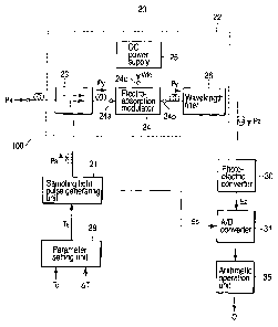
An optical signal sampling apparatus 100 according
CA 02658012 2008-12-12
29
to the invention basically includes: a sampling light
pulse generating unit 21 which generates a sampling
light pulse Ps of a predetermined period to sample an
optical signal to be sampled Px; and an optical
sampling unit 22 which samples the optical signal to be
sampled Px, with the sampling light pulse Ps from the
sampling light pulse generating unit 21 and emits an
optical pulse signal Pz obtained by the sampling,
wherein the optical sampling unit 22 includes: an
optical combiner 23 which combines the optical signal
to be sampled Px and the sampling light pulse Ps from
the sampling light pulse generating unit 21 with each
other; an electroabsorption modulator 24 having two
optical terminals 24a, 24b for inputting/outputting
light and a power supply terminal 24c for applying an
electric field to an optical path connecting the two
optical terminals 24a, 24b, the modulator having such a
characteristic that an absorption rate of the light
propagating through the optical path is changed in
accordance with the magnitude of the electric field,
one terminal 24a of the two optical terminals 24a, 24b
receiving the light Py emitted from the optical
combiner 23; a DC power supply 25 which applies, to the
power supply terminal 24c of the electroabsorption
modulator 24, a predetermined DC voltage Vdc for
sampling the optical signal to be sampled Px, with the
sampling light pulse Ps in the electroabsorption
CA 02658012 2008-12-12
modulator 24 by increasing the absorption rate in the
absence of the sampling light pulse Ps incident to the
electroabsorption modulator 24 and decreasing the
absorption rate in the presence of the sampling light
5 pulse Ps incident to the electroabsorption modulator
24, an optical signal Py' obtained by the sampling
being emitted from another terminal 24b of the two
optical terminals 24a, 24b; and an optical separator
26, 26' which selectively emits an optical signal
10 component Pz to be sampled, of the optical signal Py'
emitted from the other terminal 24b of the two optical
terminals 24a, 24b of the electroabsorption modulator
24.
An optical signal sampling method according to the
15 invention basically includes: a sampling light pulse
generating step for generating a sampling light pulse
Ps of a predetermined period to sample an optical
signal to be sampled Px; and an optical sampling step
for sampling the optical signal to be sampled Px, with
20 the sampling light pulse Ps from the sampling light
pulse generating unit 21 and emitting an optical pulse
signal Pz obtained by the sampling, wherein the optical
sampling step includes: a step of preparing an optical
combiner 23 for combining the optical signal to be
25 sampled Px and the sampling light pulse Ps with each
other; a step of preparing an electroabsorption
modulator 24 having two optical terminals 24a, 24b for
CA 02658012 2008-12-12
31
inputting/outputting light and a power supply terminal
24c for applying an electric field to an optical path
connecting the two optical terminals 24a, 24b, the
modulator having such a characteristic that an
absorption rate of the light propagating through the
optical path is changed in accordance with the
magnitude of the electric field, one terminal 24a of
the two optical terminals 24a, 24b receiving the light
Py emitted from the optical combiner 23; a step of
preparing a DC power supply 25 for applying, to the
power supply terminal 24c of the electroabsorption
modulator 24, a predetermined DC voltage Vdc for
sampling the optical signal to be sampled Px, with the
sampling light pulse Ps in the electroabsorption
modulator 24 by increasing the absorption rate in the
absence of the sampling light pulse Ps incident to the
electroabsorption modulator 24 and decreasing the
absorption rate in the presence of the sampling light
pulse Ps incident to the electroabsorption modulator
24, thereby emitting an optical signal Py' obtained by
the sampling from another terminal 24b of the two
optical terminals 24b; and a step of preparing an
optical separator 26, 26' for selectively emitting an
optical signal component Pz to be sampled, of the
optical signal Py' emitted from the other terminal 24b
of the two optical terminals 24a, 24b of the
electroabsorption modulator 24.
CA 02658012 2008-12-12
32
An optical signal monitor apparatus 20 according
to the invention basically includes: an optical signal
sampling apparatus 100 having a sampling light pulse
generating unit 21 which emits a sampling light pulse
Ps having a period different by a predetermined offset
time from an integer multiple of a clock period Tc of a
data signal modulating an optical signal to be
monitored Px; and an optical sampling unit 22 which
samples the optical signal to be monitored Px, by the
sampling light pulse Ps from the sampling light pulse
generating unit 21 and emits an optical pulse signal Pz
obtained by the sampling; and a photoelectric converter
30 which receives the optical pulse signal Pz emitted
from the optical sampling unit 22 of the optical signal
sampling apparatus 100 and converts the optical pulse
signal into an electric signal Ez thereby to acquire
waveform information of the optical signal to be
monitored Px, wherein the optical sampling unit 22 of
the optical signal sampling apparatus 100 includes: an
optical combiner 23 which combines the optical signal
to be monitored Px and the sampling light pulse Ps from
the sampling light pulse generating unit 21 with each
other; an electroabsorption modulator 24 having two
optical terminals 24a, 24b for inputting/outputting
light and a power supply terminal 24c for applying an
electric field to an optical path connecting the two
optical terminals 24a, 24b, the electroabsorption
CA 02658012 2008-12-12
33
modulator 24 having such a characteristic that an
absorption rate of the light propagating through the
optical path changes in accordance with the magnitude
of the electric field, one terminal 24a of the two
optical terminals 24a, 24b receiving the light Py
emitted from the optical combiner 23; a DC power supply
25 which increases the absorption rate in the absence
of the sampling light pulse Ps incident to the
electroabsorption modulator 24 and decreases the
absorption rate in the presence of the sampling light
pulse Ps incident to the electroabsorption modulator 24
so that the electroabsorption modulator 24 samples the
optical signal to be sampled Px, with the sampling
light pulse Ps and applies a predetermined DC voltage
Vdc to the power supply terminal 24c of the
electroabsorption modulator 24 to emit the optical
signal Py' obtained by the sampling from another
terminal 24b of the two optical terminals 24a, 24b; and
an optical separator 26, 26' which selectively emits
the optical signal component Pz to be sampled, of an
optical signal Py' emitted from the other terminal 24b
of the two optical terminals 24a, 24b of the
electroabsorption modulator 24.
An optical signal monitor method of the invention
basically includes: a sampling light pulse generating
step for emitting a sampling light pulse Ps having a
period different by a predetermined offset time from an
CA 02658012 2008-12-12
34
integer multiple of a clock period Tc of a data signal
modulating an optical signal to be monitored Px; an
optical sampling step for sampling the optical signal
to be monitored Px, by the sampling light pulse Ps and
emitting an optical pulse signal Pz obtained by the
sampling; and a photoelectric conversion step for
acquiring waveform information of the optical signal to
be monitored Px, by receiving the optical pulse signal
Pz emitted from the optical sampling unit 22 of the
optical signal sampling apparatus 100 and converting
the optical pulse signal Pz into an electric signal Ez,
wherein the optical sampling step includes: a step of
preparing an optical combiner 23 for combining the
optical signal to be monitored Px and the sampling
light pulse Ps with each other; a step of preparing an
electroabsorption modulator 24 having two optical
terminals 24a, 24b for inputting/outputting light and a
power supply terminal 24c for applying an electric
field to an optical path connecting the two optical
terminals 24a, 24b, the electroabsorption modulator 24
having such a characteristic that an absorption rate of
the light propagating through the optical path changes
in accordance with the magnitude of the electric field,
one terminal 24a of the two optical terminals 24a, 24b
receiving the light Py emitted from the optical
combiner 23; a step of preparing a DC power supply 25
for applying, to the power supply terminal 24c of the
CA 02658012 2008-12-12
electroabsorption modulator 24, a predetermined DC
voltage Vdc for sampling the optical signal to be
sampled Px, with the sampling light pulse Ps in the
electroabsorption modulator 24 by increasing the
5 absorption rate in the absence of the sampling light
pulse Ps incident to the electroabsorption modulator 24
and decreasing the absorption rate in the presence of
the sampling light pulse Ps incident to the
electroabsorption modulator 24, the optical signal Py'
10 obtained by the sampling being emitted from another
terminal 24b of the two optical terminals 24a, 24b; and
a step of preparing an optical separator 26, 26' for
selectively emitting an optical signal component Pz to
be sampled, of the optical signals Py' emitted from the
15 other terminal 24a of the two optical terminals 24a,
24b of the electroabsorption modulator 24.
The optical signal monitor apparatus 20 and method
using the optical signal sampling apparatus 100 and
method according to this invention are explained below
20 specifically with reference to FIG. 1.
The optical signal monitor apparatus 20 and method
using the optical signal sampling apparatus 100 and
method according to the invention are intended to
monitor (sample) the optical signal Px modulated with
25 the data signal having a predetermined clock period Tc
transmitted on the optical network not shown.
In a sampling light pulse generating unit 21, a
CA 02658012 2008-12-12
36
sampling light pulse Ps having a period Ts different by
a predetermined offset time AT from an integer N
multiple of a clock period Tc of a data signal
modulating the optical signal Px to be monitored
(sampled) is generated and applied to an optical
sampling unit 22.
The sampling light pulse generating unit 21 and
the optical sampling unit 22 make up the optical signal
sampling apparatus 100 according to the invention.
The sampling light pulse generating unit 21 may
have an arbitrary configuration as long as an optical
pulse of a narrow width can be generated at a
designated period Ts as described above.
FIG. 2 is a block diagram showing an example of
the sampling light pulse generating unit 21.
This sampling light pulse generating unit 21
includes a reference signal generator 21a configured as
a synthesizer for generating a stable signal Ra having
a period Ts corresponding to the period of the sampling
light pulse Ps, a multiplier 21b for multiplying the
stable signal Ra having the period Ts (frequency Fs)
generated by the reference signal generator 21a, by M
(M: integer larger than 1), and output as a signal Rb
multiplied by M, a light source 21d for emitting
continuous light Pcw, an optical modulator 21c for
emitting an optical pulse Pa having a period Ts/M by
modulating the continuous light Pcw emitted from the
CA 02658012 2008-12-12
37
light source 21d with the signal Rb M times larger than
the signal Ra, output from the multiplier 21b, an
optical gate circuit 21e for thinning the optical pulse
Pa emitted from the optical modulator 21c to 1/M and
converting it into an optical pulse Pb having a period
Ts, and a dispersion decreasing fiber 21f for further
narrowing the pulse width of the optical pulse Pb
having the period Ts converted by the optical gate
circuit 21e and emitting as the sampling light pulse
Ps.
Specifically, the reference signal generator 21a
having a configuration as a synthesizer generates the
stable signal Ra having the period Ts (frequency Fs)
designated from the parameter setting unit 28 described
later. The signal Ra thus generated is input to the
multiplier 21b and multiplied by M(M: integer larger
than 1), after which the output signal Rb is input to
the optical modulator 21c where the continuous light
Pcw emitted from the light source 21d is modulated
thereby to generate the optical pulse Pa having the
period Ts/M.
The pulse width of this optical pulse Pa is
reduced to 1/M as compared with the case in which the
continuous light Pcw is modulated directly by the
signal Ra.
The optical pulse Pa is thinned to 1/M by the
optical gate circuit 21e and, after being converted
CA 02658012 2008-12-12
38
into the optical pulse Pb of period Ts, applied to the
dispersion decreasing fiber 21f, where the pulse width
thereof is further narrowed, and finally emitted as the
sampling light pulse Ps.
The optical sampling unit 22, on the other hand,
samples the optical signal Px to be monitored
(sampled), by the sampling light pulse Ps emitted from
the sampling light pulse generator 21, and emits the
optical pulse signal Pz obtained by the sampling
operation.
The optical sampling unit 22 provides for the case
in which the wavelength of the sampling light pulse Ps
is different from that of the optical signal Px to be
monitored, and includes an optical coupler 23 as an
optical combiner, an electroabsorption modulator 24, a
DC power supply 25 and a wavelength filter 26 as an
optical separator.
The electroabsorption modulator 24, as described
above, has two optical terminals 24a, 24b for
inputting/outputting the light and a power supply
terminal 24c for applying the electric field to the
light path between the two optical terminals 24a, 24b.
The electroabsorption modulator 24 has such a
characteristic that an absorption rate of the light
propagating through the light path is changed in
accordance with the magnitude of the electric field
applied to the light path.
CA 02658012 2008-12-12
39
Normally, in the electroabsorption modulator of
this type, as disclosed in Patent Document 2, the power
supply terminal 24c is supplied with a pulse signal of
electricity for sampling.
However, it is very difficult to generate the
pulse signal of electricity having a narrow width
required to acquire the waveform information of several
tens of Gb/s described above.
In view of this, according to this embodiment, as
shown in FIG. 1, the multiplexed light Py of the
optical signal Px and the sampling light pulse Ps
having a narrow width described above is applied to the
optical terminal 24a. Also, as shown by the optical
absorption characteristic F in FIG. 3, a predetermined
DC voltage Vdc exhibits a high absorption rate a(for
example, 20 dB) in the absence of the sampling light
pulse Ps incident to the optical terminal 24a, while in
the presence of the incident sampling light pulse Ps,
on the other hand, the DC voltage Vdc assumes a low
absorption rate R(for example, 3 dB) due to the mutual
absorption saturation characteristic. This DC voltage
Vdc is applied from the DC power supply 25 to the power
supply terminal 24c.
The characteristic F of FIG. 3 is shown as a
model.
As a result, only in the presence of the incident
sampling light pulse Ps, the absorption rate of the
CA 02658012 2008-12-12
electroabsorption modulator 24 is reduced and the
multiplexed light Py' is emitted from the other optical
terminal 24b.
Since the multiplexed light Py' contains also the
5 component of the sampling light pulse Ps, only the
wavelength component of the optical signal Px is
extracted from the multiplexed light Py' by the
wavelength filter 26 constituting an optical separator,
and emitted as an optical pulse signal Pz.
10 In the process, the sampling efficiency is
determined by the insertion loss of the
electroabsorption modulator 24 and about -10 dB, which
is improved 10 dB or more than in the case where the
bulk-type nonlinear optical member is used.
15 Also, the period Ts of the sampling light pulse Ps
and the sampling clock Es output from the sampling
light pulse generator 21 is set by the parameter
setting unit 28.
The parameter setting unit 28, receiving the
20 information on the offset time AT and the clock period
Tc (which may alternatively be the bit rate) of the
data signal modulating the optical signal Px to be
monitored, determines the sampling period Ts by the
arithmetic operation
25 Ts = N=Tc + AT
and this value is set in the sampling light pulse
generating unit 21.
CA 02658012 2008-12-12
41
The value N is determined by the variable
frequency range of the signal adapted to be output from
the sampling light pulse generating unit 21 and the
clock period Tc of the data signal.
Assume, for example, that AT is negligibly small
as compared with Ts, Tc is about 0.1 ns (10 GHz) and Ts
is variable in the neighborhood of 0.1 s (10 MHz), the
value N is about Ts/Tc = 1000.
The optical pulse signal Pz emitted from the
sampling unit 22 enters the photoelectric converter 30
and is converted to the electric signal Ez.
The output signal Ez from the photoelectric
converter 30, after sampled and converted to a digital
value by an analog/digital (A/D) converter 31, is input
to an arithmetic operation unit 35.
The sampling operation of the A/D converter 31 is
performed by the sampling clock Es in synchronism with
the sampling light pulse Ps.
According to this embodiment, this electricity
sampling clock Es is also output from the sampling
light pulse generating unit 21 (the reference signal
generator 21a described above).
The arithmetic operation unit 35, based on the
signal Ez converted to a digital value by the A/D
converter 31, calculates the value indicating the
quality of the optical signal Px to be monitored.
This arithmetic operation, is arbitrary performed
CA 02658012 2008-12-12
42
in such a manner that, as described in Patent Document
1, for example, the signal Ez is retrieved as a sample
value for a predetermined time, and after being
compared with a predetermined threshold value,
separated into a sample value associated with the data
"l" and a sample value associated with the data "0".
For each of these data, the average values and the
standard deviations of the sample value group are
determined, and the quality value Q is determined as a
ratio /y between the difference of the average
values and the sum y of the standard deviations.
Incidentally, the larger the value Q, the higher
the signal quality of the optical signal Px to be
monitored.
The quality value Q is calculated, for example, at
predetermined time intervals, and the result thereof is
notified to an outward device at a predetermined
timing.
The value indicating the signal quality of the
optical signal Px to be monitored is not limited to the
Q value, but may be another statistic quantity.
Next, an explanation is given about the relation
between the waveform of the optical signal Px to be
monitored and the acquisition timing thereof required
to calculate the value indicating the quality of the
optical signal Px to be monitored.
In the case where the optical signal Px to be
CA 02658012 2008-12-12
43
monitored is used for testing and repeatedly modulated
for a predetermined code string of a predetermined bit
length L as shown in (a) of FIG. 4, then the value N
determining the period Ts of the sampling light pulse
Ps is made equal to K times (K: integer) the bit length
L as shown in (b) of FIG. 4. In this way, the
repetitive waveform of the optical signal Px can be
sampled in time series at intervals of AT as shown in
(c) of FIG. 4.
This sampling operation is performed U=Tc/AT times
(U: integer) continuously as shown in (d) of FIG. 4.
Thus, the waveform data of U bits can be obtained in
time series from the sampling start timing.
The optical signal Px actually transmitted on the
optical network is not necessarily a repetitive
waveform as shown in (a) of FIG. 5.
Assume that this optical signal Px is sampled with
a period Ts equal to N=Tc + AT as shown in (b) of
FIG. 5. In view of the fact that the data for every N
bits of the optical signal Px are sampled at timings
different by AT, respectively, the value obtained by
sampling has an amplitude corresponding to the data
NNl", "0" or an amplitude in transition state between
the data, as shown in (c) of FIG. 5. Therefore, the
sampling result on the waveform continuous for a
predetermined period of the optical signal Px is not
obtained.
CA 02658012 2008-12-12
44
By the continuous sampling operation for a
predetermined number of plural bits as described above
and thus obtaining the statistic quantity thereof, the
quality value Q can be determined.
Also, in an application to the sync sampling, on
the other hand, the sampling result for plural bits is
superposed over the 1-bit width. In this way, an eye
pattern as shown in (d) of FIG. 5 is obtained, and the
signal quality may be determined from this eye pattern.
Incidentally, in the case where the sampling
period is displaced from the bit rate of the data
signal modulating the optical signal (asynchronous
state), the observed waveform obtained by superposition
would be deviated and the eye pattern could not be
observed.
By the sampling operation at predetermined time
period as described, however, the statistic quantity
and the quality value Q can be obtained.
(Second embodiment)
FIG. 6 is a block diagram shown for explaining the
configuration of the optical signal sync sampling
apparatus 100 and the optical signal monitor apparatus
20' using the sampling apparatus 100 according to a
second embodiment of the invention.
An example of the configuration of the optical
signal monitor apparatus 20' always capable of holding
the synchronous state is shown in FIG. 6.
CA 02658012 2008-12-12
In the optical signal monitor apparatus 20', the
sampling light pulse generating unit 21, the optical
sampling apparatus 22, the parameter setting unit 28,
the photoelectric converter 30 and the A/D converter 31
5 are equivalent to the corresponding component parts of
the first embodiment and therefore not described again.
In the optical signal monitor apparatus 20', the
output signal Ez of the photoelectric converter 30 is
input to the fundamental wave component signal output
10 unit 41.
The fundamental wave component signal output unit
41 is for outputting the fundamental wave component
signal U having a frequency equal to that of the
fundamental wave component of the envelope wave of the
15 signal Ez output in pulse form from the photoelectric
converter 30.
The fundamental wave component signal output unit
41 may be formed of either a filter type or PLL (phase-
locked loop) type.
20 In the filter type, the sinusoidal fundamental
wave component signal U is extracted by a narrow-band
bandpass filter having the central frequency (for RZ
scheme) equal to the clock frequency Fc of the data
signal modulating the optical signal or the central
25 frequency (for NRZ scheme) twice as high as the clock
frequency Fc.
In the PLL type, on the other hand, as shown in
CA 02658012 2008-12-12
46
FIG. 7, the output signal of the narrow-band bandpass
filter 41a described above and the output signal of a
voltage controlled oscillator 41b are input to a phase
comparator 41c, and the oscillation frequency of the
voltage-controlled oscillator 41b is controlled by the
control signal Vc corresponding to the phase difference
between the two output signals. In this way, the phase
of the oscillation output signal is synchronized with
the output signal of the bandpass filter 41a, and this
synchronous sinusoidal oscillation output signal is
used as the fundamental wave component signal U.
As another example, the output signal Ez of the
photoelectric converter 30 is input to a fast Fourier
transform (FFT) operation unit for frequency analysis
thereby to determine the frequency of the fundamental
wave component. The fundamental wave component signal
U having a frequency equal to the frequency thus
determined is generated and output from a signal
generator.
Assuming that the clock frequency Fc of the
optical signal Px is 10 GHz and the offset time AT is
0.1 ps, 1000 sampling sessions are required to obtain
the 1-bit waveform data of the optical signal Px. The
time required for conducting the 1000 sampling sessions
with the frequency Fs of about 10 MHz is approximately
0.1 ms. This time is equal to the period of the
fundamental wave component of the envelope wave of the
CA 02658012 2008-12-12
47
signal Ez having the frequency of about 10 kHz.
The fundamental wave component signal U is input
to the comparator 42 and compared with the threshold
value Vr preset by a threshold value setter 43. The
comparison result is input to a data acquisition
control unit 44.
The data acquisition control unit 44, based on the
output signal of the comparator 42, writes the data
signal Dz of the A/D converter 31 in a waveform memory
45.
Specifically, from the timing when the fundamental
wave component signal U exceeds the threshold value Vr
upward, for example, the data signal Dz starts to be
written into the waveform memory 45, and upon complete
writing of a predetermined number W of the data signal,
the operation stands by until the timing when the
fundamental wave component signal U exceeds the
threshold value Vr upward. This operation is repeated
a predetermined number H of times.
Incidentally, the predetermined number W of the
data signal Dz are written at H different plural areas
of the waveform memory 45 in the order of the address.
The arithmetic operation unit 35', like the
arithmetic operation unit 35 according to the first
embodiment, calculates the value indicating the quality
of the optical signal Px to be monitored, based on the
data signal Dz written in the waveform memory 45.
CA 02658012 2008-12-12
48
Next, the relation between the waveform of the
optical signal Px to be monitored and the acquisition
timing thereof according to the second embodiment is
explained.
In the case where the optical signal Px to be
monitored is for test operation, for example, and
repeatedly modulated in a predetermined code string of
a predetermined bit length L as shown in (a) of FIG. 8,
then, as shown in (b) of FIG. 8, the sampling operation
is performed while the value N determining the period
Ts of the sampling light pulse Ps is equal to a value K
(K: integer) times larger than the bit length L. In
this way, as shown in (c) and (d) of FIG. 8, an optical
pulse Pz having an envelope waveform of an enlarged
time axis of the optical signal Px is obtained.
Then, from the light receiving signal Ez of this
optical pulse signal Pz, the sinusoidal fundamental
wave component signal U as shown in (e) of FIG. 8 is
obtained.
From the timing when the fundamental wave
component signal U exceeds the threshold value Vr, the
data acquisition is started as shown in (f) of FIG. 8,
so that the data for J=Tc/OT times sampling operations
(U: integer) is acquired.
The arithmetic operation described above is
performed on this J-bit waveform data thereby to
determine the Q value.
CA 02658012 2008-12-12
49
Incidentally, the time axis is shown in shorter
scale in (d) to (f) of FIG. 8.
In obtaining eye patterns, on the other hand, as
shown in (d) to (f) of FIG. 8, the waveform data
acquisition is started from the timing when the
fundamental wave component signal U exceeds the
threshold value Vr, so that the process for J bits is
executed plural times and stored in different areas 1
to H of the waveform memory 45 as shown in FIG. 9.
These waveform data Dz in the plural areas are
superposed in the order of the address thereby to
obtain the eye pattern as shown in FIG. 10.
The head data of these waveform data is equal to a
value sampled immediately after the timing when the
fundamental wave component signal U exceeds the
threshold value Vr and synchronized exactly with the
data signal. Therefore, the time axis of the waveform
data superposed is not greatly displaced, and the
amplitude variation of the optical signal is expressed
substantially accurately.
The relation between the quality and the position
in the bit is determined on this eye pattern.
For example, the value Q is calculated based on
the sample value at an intermediate point L
(intermediate point of 1 bit) of two cross points as
shown in FIG. 10, and together with the Q value of the
whole data irrespective of the position described
CA 02658012 2008-12-12
above, notified to other devices through a
communication means not shown.
Incidentally, the optical signal Px actually
transmitted on the optical network is not limited to
5 the repetitive waveform shown in (a) of FIG. 11.
In the case where this optical signal Px is
sampled with the period Ts equal to N=Tc + AT as shown
in (b) of FIG. 11, the sample timing is different by AT
for every N bits of the optical signal Px. Thus, the
10 peak value of the optical pulse signal Pz obtained by
the sampling, as shown in (c) of FIG. 11 and (d) of
FIG. 11 on a shorter time scale, is either the
amplitude corresponding to the data "1", "0" or the
amplitude in the transition state therebetween. Thus,
15 the envelope wave of an enlarged continuous waveform
for a predetermined period of the optical signal Px is
not obtained.
This envelope wave contains the fundamental wave
component of the data signal modulating the optical
20 signal Px, and this fundamental wave component signal U
is obtained as shown in (e) of FIG. 11.
As in the case described above, the data
acquisition is started as shown in (f) of FIG. 11 at
the timing when the fundamental wave component signal U
25 exceeds the threshold value Vr, and the data is
acquired by J-Tc/AT times sample sessions (U: integer)
The Q value can be determined by performing a
CA 02658012 2008-12-12
51
similar arithmetic operation described above on the
J-bit waveform data.
Incidentally, the time axis is shown in shorter
scale in (d) to (f) of FIG. 11.
This J-bit waveform data itself may be said to
indicate the eye pattern. To obtain an eye pattern
accurately indicating the quality of the optical signal
using a greater number of sample values, however, as
shown in (d) to (f) of FIG. 11, the acquisition of the
waveform data is started from the timing when the
fundamental wave component signal U exceeds the
threshold value Vr and conducted for J bits. This
process is repeated H times and as in the
aforementioned case, stored in different areas 1 to H
of the waveform memory 45. By superposing this data in
the order of address, an accurate eye pattern can be
obtained.
Also in this case, the head data of each waveform
data has a value sampled immediately after the timing
when the fundamental wave component signal U exceeds
the threshold value Vr and is accurately synchronized
with the data signal. Thus, the waveform data is not
superposed with the time axis greatly displaced, and
indicates the amplitude variation of the optical signal
in substantially accurate manner.
The optical sampling unit 22 used for the optical
signal monitor apparatus 20, 20' according to each
CA 02658012 2008-12-12
52
embodiment described above includes the
electroabsorption modulator 24 as a sampling element.
One of the optical terminals of the modulator 24 is
supplied with the multiplexed signal of the optical
signal to be sampled and the sampling light pulse. The
power supply terminal, on the other hand, is supplied
with a predetermined DC voltage indicating a high
absorption rate in the absence of the incident sampling
light pulse and a low absorption rate in the presence
of the incident sampling light pulse, so that in the
presence of the incident sampling light pulse, the
component of the optical signal is selectively emitted
from the light from the other optical terminal.
As a result, the optical pulse having a narrow
width can be used for sampling, and in addition, the
loss of the optical signal can be reduced. Thus, the
sampling efficiency is substantively improved, and the
accurate waveform information can be obtained even for
a weak optical signal.
Also, in the case where the fundamental wave
component signal U is obtained from the signal produced
by sampling and the timing to start the waveform
acquisition is synchronized as in the optical signal
monitor apparatus 20' according to the second
embodiment, the time axis is not likely to be displaced
greatly and the eye pattern of the optical signal can
be obtained in stable fashion even when the data
CA 02658012 2008-12-12
53
signals Dz acquired for different periods are
superposed.
Incidentally, instead of determining the quality
value or the eye pattern through the arithmetic
operation unit 35, 35' as in the first and second
embodiments, the arithmetic operation unit 35' may be
done without and the data written in each area of the
waveform memory 45 may be transmitted to an external
device through a communication means not shown thereby
to display the arithmetic operation on the quality and
the eye pattern on the particular external device.
In the optical sampling unit 22 used for the
optical signal monitor apparatus 20, 20' according to
the first and second embodiments, the optical signal Px
and the sampling light pulse Ps of different
wavelengths are multiplexed with each other and applied
to one optical terminal 24a of the electroabsorption
modulator 24, while the wavelength component of the
optical signal is separated and extracted from the
light emitted from the other optical terminal 24b
thereby to sample the optical signal.
It is also possible, as in the third embodiment
described later, to sample the optical signal
irrespective of the wavelength by controlling the
polarized waves of the optical signal Px to be
monitored and the sampling light pulse Ps.
Also, in the sampling light pulse generating unit
CA 02658012 2008-12-12
54
21 making up the optical signal sampling apparatus 100
used for the optical signal monitor apparatus 20, 20'
according to the first and second embodiments, the
optical pulse having a narrow width is generated as the
sampling light pulse Ps for sampling the optical signal
Px to be monitored, with the period Ts = N=Tc + AT
designated by the parameter setting unit 28. The
repetitive waveform of the optical signal Px to be
monitored is then sampled at time intervals of, for
example, AT in time series as shown in (c) of FIG. 4.
At the same time, as shown in (d) of FIG. 4, the
optical signal Px is sampled U=Tc/AT times (U: integer)
continuously thereby to obtain the waveform data of U
bits in time series from the sampling start timing.
Specifically, in this case, the time axis of the
waveform data finally obtained is calibrated into a
state desirable for evaluation of the waveform data.
On the other hand, this gives rise to the requirement
of an expensive sampling light pulse generating unit 21
having a complicated configuration as shown in FIG. 2.
Nevertheless, the calibration of the time axis of
the waveform data finally obtained may not be required
in some case as an optical signal monitor apparatus.
In such a case, as in the fourth and fifth embodiments
described later, an inexpensive sampling light pulse
generating unit having a simple configuration may be
used in place of the expensive sampling light pulse
CA 02658012 2008-12-12
generating unit 21 having a complicated configuration
as shown in FIG. 2.
(Third embodiment)
FIG. 12 is a block diagram shown for explaining
5 the configuration of the optical signal sampling
apparatus 100A and the optical signal monitor apparatus
20A using the apparatus 100A according to the third
embodiment of the invention.
Specifically, in the optical sampling unit 22A
10 making up the optical signal sampling apparatus 100A
shown in FIG. 12, the optical signal Px to be monitored
enters the polarized wave controller 23a, and the
direction of polarization thereof is set orthogonal to
the direction of polarization of the sampling light
15 pulse Ps, after which the resulting light, together
with the sampling light pulse Ps, is applied to and
multiplexed in the optical coupler 23b of polarization
multiplexing type making up the optical combiner 23.
The multiplexed light Py' is applied to one optical
20 terminal 24a of the electroabsorption modulator 24, and
among the light rays emitted from the other optical
terminal 24b, only the polarized component Pz of the
optical signal Px is selected by the polarization
filter 26' as an optical separator.
25 The sampling light pulse generating unit 21 of
this optical signal monitor apparatus 20A generates the
sampling light pulse Ps having the direction of
CA 02658012 2008-12-12
56
polarization orthogonal to the direction of
polarization of the optical signal Px to be monitored.
As the polarized wave controller 23a, any one of
the polarization controller, the polarization plate and
the polarized beam splitter can be used. Also, as the
polarization filter 26', the polarization plate or the
polarized beam splitter can be used.
The other elements of the configuration of the
optical signal monitor apparatus 20A is equivalent to
that of the first and second embodiments, and
therefore, not explained again.
(Fourth embodiment)
FIG. 13 is a block diagram shown for explaining
the configuration of the optical signal sampling
apparatus 100B and the optical signal monitor apparatus
20B using the apparatus 100B according to the fourth
embodiment of the invention.
Specifically, the sampling light pulse generating
unit 21B making up the optical signal sampling
apparatus 100B shown in FIG. 13, in which the time axis
of the waveform data finally obtained is not required
to be calibrated, is configured of a short pulse
generating unit 21g which has the function of self-
oscillating a short pulse Ps' having the frequency
different by one integer-th from the frequency of the
optical signal Px to be sampled on the one hand and
shifting the frequency of the short pulse Ps' by about
CA 02658012 2008-12-12
57
5% (5 kHz, for example) of the frequency (10 MHz, for
example) of the short pulse Ps' on the other hand.
This short pulse generating unit 21g may be, for
example, a mode lock fiber laser (MLFL) disclosed in
Patent Document 3 described above and can realize an
inexpensive sampling light pulse generating unit having
a simple configuration.
The other elements of the configuration of this
optical signal monitor apparatus 20B is equivalent to
those of the first embodiment shown in FIG. 1, and
therefore, not described again (except that the
parameter setting unit 28 is not required).
(Fifth embodiment)
FIG. 14 is a block diagram shown for explaining
the configuration of the optical signal sampling
apparatus 100C and the optical signal monitor apparatus
20C using the apparatus 100C according to the fifth
embodiment of the invention.
Specifically, the sampling light pulse generating
unit 21C making up the optical signal sampling
apparatus 100C shown in FIG. 14, in which the time axis
of the waveform data finally obtained is not required
to be calibrated, is configured of a short pulse
generating unit 21g which has the function of self-
oscillating a short pulse having the frequency
different by one integer-th from the frequency of the
optical signal Px to be sampled on the one hand and
CA 02658012 2008-12-12
58
shifting the frequency of the short pulse on the other
hand.
This short pulse generating unit 21g may be, for
example, a mode lock fiber laser (MLFL) disclosed in
Patent Document 3 described above and can realize an
inexpensive sampling light pulse generating unit having
a simple configuration.
The other elements of the configuration of this
optical signal monitor apparatus 20C is equivalent to
those of the second embodiment shown in FIG. 6, and
therefore, not described again (except that the
parameter setting unit 28 is not required).
As described in detail above, according to this
invention, there are provided an optical signal
sampling apparatus and method for solving the problems
of the prior art, having a high sampling efficiency and
capable of sampling the waveform information of a fast
optical signal accurately with a sufficient resolution,
and an optical signal monitor apparatus and method
capable of accurately monitoring the optical signal and
obtaining an eye pattern of the optical signal in
stable fashion using the optical signal sampling
apparatus and method.