Note : Les descriptions sont présentées dans la langue officielle dans laquelle elles ont été soumises.
t S CA 02663563 2009-03-12
1
Anti-intrusion system for protecting electronic components
The field of the invention is that of anti-intrusion systems for the
protection of electronic components and their application in the
telecommunications field.
The aim of an anti-intrusion system is to detect any attempted
intrusion into the electronic device to be protected and activate a warning
system where appropriate. The anti-intrusion systems are used to protect
electronic devices for which confidentiality is to be maintained.
According to the state of the art in anti-intrusion systems, the
protection can be provided by using an enclosure comprising a network of
conducting wires integrated in a resin. An intrusion evidenced by a
perforation of the enclosure is then detected by the appearance of a break in
the conducting wires. This type of system does not give full satisfaction in
its
performance, notably because it does not protect against an intrusion using
X-rays.
The invention, notably to overcome the problem of intrusion by
X-radiation, proposes to use an entirely conducting enclosure, consisting of
electromagnetic shielding and comprising microcomponents used to detect
intrusions.
More specifically, the invention relates to an anti-intrusion system
for protecting electronic components comprising a substrate on which the
electronic components are placed, a conducting enclosure encapsulating the
electronic components on the surface of the substrate, said system also
including a warning device, characterized in that it comprises at least: an
encapsulated intrusion detection circuit in said enclosure, said intrusion
detection circuit comprising at least:
- a transmitting antenna situated on the surface of the
substrate and transmitting a power signal,
- a capacitive electromechanical microswitch associated
with means of receiving said power signal and said
microswitch being able to detect a signal power drop and,
where appropriate, activate an intrusion warning device,
- means of receiving the transmitted signal, said reception
means transmitting a signal drop on an intrusion into the
enclosure, said reception means being linked to said
CA 02663563 2009-03-12
2
microswitch.
According to a first variant of the invention, the reception means
comprise: a receiving antenna situated on the surface of the substrate and
linked to the capacitive electromechanical microswitch.
According to a second variant of the invention, the reception
means comprise: a conducting element linked to the conducting enclosure
and to the capacitive electromechanical microswitch.
According to a third variant of the invention, the reception means
comprise:
- a receiving antenna situated on the surface of the
substrate and linked to a first capacitive electromechanical
microswitch;
- a conducting element linked to the conducting enclosure
and to a second capacitive electromechanical microswitch.
According to a variant of the invention, at least one of the
capacitive electromechanical microswitches is of series type.
According to a variant of the invention, at least one of the
electromechanical microswitches comprises a structure including a flexible
membrane and an assembly comprising a dielectric layer, and two signal
lines positioned coplanar in the extension of each other and the ends of
which form a first metallic layer, said membrane being separated from the
assembly by a dielectric gap.
According to a variant of the invention, the transmitting antenna
transmits a power signal such that the voltage Veq applied between the
membrane and the electrode is between an activation voltage Vp and a
release voltage Vr, said activation and release voltages respectively
satisfying the following equations:
o
V = g
P 27sowW
where w is the width of the signal fines, W is the width of the
membrane, go is the thickness of the dielectric gap without voltage
applied to the membrane, Eo: the permittivity of the vacuum and k
the stiffness coefficient of the membrane.
CA 02663563 2009-03-12
3
/2k(gQ_td)ta
V r 0A
r
where td is the dielectric thickness separating the metallic layer
from the membrane, Er the relative permittivity of the dielectric, A
is equal to the product wW and E' is a constant making it possible
to take account of the effect of the presence of the dielectric gap
which modifies the permittivity of the electrodes.
Advantageously, the transmitting and receiving antennas are of
bidirectional type.
The invention will be better understood and other benefits will
become apparent from reading the description that follows, given by way of
nonlimiting example, and from the appended figures in which:
= figure 1 illustrates a first anti-intrusion system variant
according to the invention comprising at least one receiving
antenna linked to a capacitive electromechanical
microswitch, seen in cross section;
= figure 2 illustrates the first anti-intrusion system variant
according to the invention seen from above inside the
enclosure;
= figure 3 illustrates a capactive electromechanical
microswitch of series type seen from above;
= figure 4 illustrates the series-type capacitive
electromechanical microswitch seen in cross section;
= figure 5 illustrates the trend of the thickness of the dielectric
gap as a function of the voltage applied to the series-type
capacitive electromechanical microswitch when it is
actuated.
= figure 6 illustrates a second anti-intrusion system variant
according to the invention, with an electromechanical
microswitch linked to the conducting enclosure by a
conducting element, seen in cross section;
= figure 7 illustrates a part of the second anti-intrusion system
variant according to the invention, seen from above inside
the enclosure;
= figure 8 illustrates a third anti-intrusion system variant
CA 02663563 2009-03-12
4
according to the invention, comprising at least one receiving
antenna linked to a first capacitive electromechanical
microswitch and a second capacitive electromechanical
microswitch linked to the conducting enclosure by a
conducting element, seen in cross section.
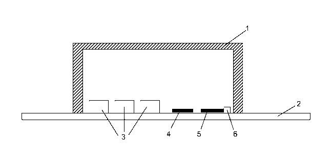
The anti-intrusion system for protecting electronic components 3
according to the invention comprises a substrate 2 on which the electronic
components are placed, a conducting enclosure 1 encapsulating the
1 o electronic components on the surface of the substrate 2. The intrusion
detection circuit is encapsulated in said enclosure 1. It comprises at least:
a transmitting antenna 4 situated on the surface of the substrate 2
and transmitting a signal,
a capacitive electromechanical microswitch, said microswitch
being linked to the warning device by a signal line, so as to be able to
activate it, said microswitch being able to detect a signal power drop, and
means of receiving the transmitted signal, said reception means
transmitting a signal drop on an intrusion into the enclosure, said reception
means being linked to said microswitch.
Any intrusion or attack on the physical integrity of the conducting
enclosure 1 leads to a disturbance of the transmission of the signal from the
transmitting antenna 4 to the reception means, so reducing the power of the
signal transmitted and provoking a change of the state of the microswitch.
A first variant of an anti-intrusion system for protecting electronic
components according to the invention using a series-type capacitive
electromechanical microswitch is illustrated in figures 1 and 2.
The first variant of the system according to the invention
comprises a hermetic and conducting enclosure 1 on the surface of a
substrate 2, a transmitting antenna 4, a receiving antenna 5 linked to the
warning system, not represented, by two transmission lines 7 and 8 above
which there is a series-type capacitive electromechanical microswitch 6.
The anti-intrusion system works as follows. The system uses the
variations of a reference signal, generated by a violation of the hermetic and
conducting enclosure 1, to trigger the warning device. In practice, the system
is armed by operating the series-type capacitive electromechanical
CA 02663563 2009-03-12
microswitch 6 by placing it in the low state, the conducting state. A signal
is
then sent through the transmitting antenna 4, which is received by the
receiving antenna 5 then transmitted to the warning device via the
transmission lines 7 and 8. The warning device is configured to be triggered
5 when it no longer receives a signal. Moreover, the power of this signal is
determined in such a way as to maintain the series-type capacitive
electromechanical microswitch 6 in the low (conducting) state according to
the principle that will be explained in the next paragraph and that will be
called self-maintenance. Any intrusion or attack on the physical integrity of
lo the conducting enclosure 1 leads to a disturbance of the transmission of
the
signal from the transmitting antenna 4 to the receiving antenna 5, so reducing
the power of the transmitted signal. This power reduction in the signal
passing through the series-type capacitive electromechanical microswitch 6
provokes its transition to the high state (non-conducting). The warning device
connected to the output of the series-type capacitive electromechanical
microswitch 6 no longer receives any signal and is triggered.
There now follows a more detailed description of a series-type
microswitch structure comprising:
= A flexible membrane,
= A dielectric layer,
= A metallic layer.
Figure 3 represents a top view of such a microswitch and figure 4
represents a cross-section view.
The structure of the first microswitch in series comprises: a first
signal line 107 (linked to the signal line 7) and a second signal line 108
(linked to the signal line 8) positioned coplanar in the extension of each
other,
separated by a switching zone, the ends of which form a metallic layer 105
which acts as a bottom electrode, positioned on the substrate 2, a dielectric
material 104 placed on the metallic layer 105. A membrane 101 overhangs
the signal lines, linking the pillars 102 and 103 placed on the substrate. The
membrane is insulated from the ground plane 9.
The microswitch works as follows:
The application of an activation voltage under the membrane 101
changes it from an open, non-conducting rest state, to the closed,
conducting, state. The microswitch has specific means (not described) for
CA 02663563 2009-03-12
6
imposing a potential difference between the metallic layer 105 and the
membrane 101. Under the effect of the activation voltage, the membrane is
deformed until it touches the dielectric 104. The two signal lines 107 and 108
are then interlinked by capacitive effect. Figure 5 illustrates the trend of
the
thickness of the dielectric gap as a function of the voltage applied to the
series-type capacitive electromechanical microswitch when it is operated, go
is the initial thickness of the dielectric gap between the membrane 101 and
the diefectric 104.
The series microswitch is characterized by two voltages: Vp, the
lo activation voltage and Vr the release voltage. Vp is determined by the
following equation:
V = gkg0
27cowW
where w is the width of the signal lines, W the width of the
membrane (the product wW then represents the surface area facing the
signal lines and the membrane), go is the thickness of the dielectric gap with
no voltage applied, F-o: the permittivity of the vacuum and k the stiffness
coefficient of the membrane.
Vr is determined by the following equation:
V_ 2k(go - t ZYd
S'S~ABr
where td is the dielectric thickness separating the line from the
membrane and s, the relative permittivity of the dielectric, A is equal to the
product wW and s' is a constant making it possible to take account of the
effect of the presence of the dielectric gap which modifies the permittivity
of
the electrodes.
The s' coefficient is between 0.4 and O.B. It can be determined
empirically by comparing the results of measurements with the theoretical
calculation of a plane capacitance.
Let P be the power of the signal passing through the series
microswitch and Veq the mean voltage corresponding to this power. The
following relationship then applies:
CA 02663563 2009-03-12
7
z
P Ve9
R
where R is the impedance of the signal line. The series
microswitch can be in three possible states:
= Veq > Vp: this represents the self-actuation state. This means that
the simple fact of passing the signal through the microswitch
provokes its transition to the low state, the conducting state.
= Vr < Veq < Vp: this represents the self-maintaining state. This
means that the simple fact of passing the signal through the
microswitch prevents the membrane from rising again after
actuation.
= Veq < Vr, the microswitch operates in a simple manner, the signal
does not disrupt the operation of the microswitch which is in the
high, non-conducting, state.
For the anti-intrusion system according to the invention, the power
of the signal is dimensioned such that the limit of the second and of the
third
cases applies. The microswitch can then switch from the self-maintaining
state to the high state if there is a slight reduction in the power of the
signal.
Advantageously, at least one of the electromechanical
microswitches comprises a second metal layer 106 situated on the dielectric
104. The benefit of the second metallic layer 106 is to overcome the problem
of electrical discharge which ultimately takes place over time on the
dielectric
layer 104, representing a degradation to the level of the detection of the
variations of power of the signal.
There now follows a description of a second anti-intrusion system
variant according to the invention, illustrated notably by figures 6 and 7,
where an electromechanical microswitch 32 is linked to the conducting
enclosure 1 by a first conducting element 31. Also, the electromechanical
microswitch 32 is linked to the warning device by a second conducting
element 34.
The second anti-intrusion system variant works as follows. The
system uses the disturbances of the eddy currents generated by the antenna
33 on the enclosure. A violation of the enclosure is reflected in a variation
of
these eddy currents. As in the first anti-intrusion system variant, it is this
CA 02663563 2009-03-12
8
variation that will be used to change the state of the electromechanical
microswitch 32. The lowering of the power of the signal passing through the
signal switches it from a low (conducting) state to a high (non-conducting)
state which causes the warning device, configured to be triggered when it no
longer receives any signal, to be activated.
There now follows a description of a third anti-intrusion system
variant according to the invention using the two preceding variants in
parallel.
The third anti-intrusion system variant according to the invention comprises a
hermetic and conducting enclosure 1 placed on a substrate 2; a first
1 o detection assembly comprising a transmitting antenna 84, a receiving
antenna 85 linked to the waming system, not represented, by a transmission
line, not represented, above which there is a first series-type capacitive
electromechanical microswitch 86 and a second detection assembly
comprising a second series-type capacitive electromechanical microswitch
82 linked to the hermetic and conducting enclosure 1 by a first conducting
element 81 and linked to the warning device by a second conducting
element, not represented.
The third anti-intrusion system variant works as follows. The two
detection assemblies operate in parallel. The first detection assembly
corresponds to the first detection system variant. The second detection
assembly corresponds to the second detection system variant. The two
detection assemblies can use the same transmitting antenna 84.
Advantageously, at least one of the conducting elements is
situated on the surface of the substrate 2.
Advantageously, the transmitting and receiving antennas are of
bidirectional type.
According to an exemplary embodiment of an electromechanical
microswitch for a protection system according to the invention, the
membrane 101 has a thickness of 0.7 pm consisting of two metallic layers: a
first aluminum layer of 0.5 pm and a second titanium-tungsten alloy layer of
0.2 pm. The membrane 101 presents a width of approximately 100 pm and a
length dependent on the coplanar line.
CA 02663563 2009-03-12
9
A coplanar line is a microwave signal conductor consisting of a
substrate (generally of silicon, given its low cost and the little influence
that
the quality of the substrate can have on the performance of a coplanar line)
on which there is a metallic conducting line (generally of gold) and two
ground planes situated either side of this line (generally also of gold). A
coplanar line is defined by: the thickness of the line and of the ground
planes,
the width of the central line and the distance separating the central line
from
the ground planes. A symmetrical structure relative to the central line is
thus
obtained.
The coplanar lines 107 and 108 that serve as a support for the
capacitive electromechanical microswitch have a thickness of 3 pm, they are
refined under the membrane to a thickness of 0.7 pm. They are covered in
this location by a dielectric of a thickness varying between 0.2 and 0.4 pm.
The pillars 102 and 103, 3 pm high, are positioned either side of
the signal lines 107 and 108 to serve as a support for the membrane 101 and
are independent of the ground 9 which is hollowed out in order to be able to
have the pillars 102 and 103 at the same level as said ground. The space
separating the signal lines 107 and 108 is 10 pm.