Note : Les descriptions sont présentées dans la langue officielle dans laquelle elles ont été soumises.
CA 02669581 2009-05-14
DESCRIPTION
Silicon Carbide Semiconductor Device and Method of Manufacturing the Same
TECHNICAL FIELD
The present invention relates to a silicon carbide semiconductor device
including
an extended terrace portion and a method of manufacturing the same.
BACKGROUND ART
Semiconductor devices such as transistors or diodes formed by using a silicon
carbide substrate (SIC substrate) where Si and C are bonded at a component
ratio of 1: 1
are expected to be put to practical use as power devices. Since silicon
carbide is a
wide band gap semiconductor and a breakdown electric field thereof is an order
of
magnitude higher than that of silicon, a high reverse breakdown voltage can be
maintained even if the thickness of a depletion layer in a pn junction or a
Schottky
junction is reduced. Thus, the use of the silicon carbide substrate allows the
thickness
of the device to be reduced and a doping concentration to be increased.
Therefore, it is
expected that a low-loss power device having low on-resistance and high
breakdown
voltage will be realized. A substrate having a 4H or 6H polytype is generally
used as
the silicon carbide substrate, and in order to achieve smooth epitaxial
growth, a
substrate having a main surface offset at approximately 8 with respect to a{
0001 }
surface is used.
Vertical MOSFETs (Metal Oxide Semiconductor Field Effect Transistors) where
a current is vertically flown in order that a surface of a silicon carbide
layer may be
effectively used are the mainstream in MOSFETs formed by using a silicon
carbide
substrate. One of the vertical MOSFETs that are known is a so-called UMOSFET
(that is also referred to as a trench-type MOSFET) having a trench formed in a
part of a
silicon carbide layer and a gate electrode formed in the trench. This is a
transistor
where a channel region is provided vertically. Examples of the UMOSFET are
-1-
CA 02669581 2009-05-14
disclosed, for example, in Japanese Patent Laying-Open No. 10-125904 (Patent
Document 1), Japanese Patent Laying-Open No. 2005-56868 (Patent Document 2)
and
Japanese Patent Laying-Open No. 2005-340685 (Patent Document 3).
Patent Document 1: Japanese Patent Laying-Open No. 10-125904
Patent Document 2: Japanese Patent Laying-Open No. 2005-56868
Patent Document 3: Japanese Patent Laying-Open No. 2005-340685
DISCLOSURE OF TIE INVENTION
PROBLEMS TO BE SOLVED BY THE INVENTION
In power devices that are the mainstream in silicon carbide semiconductor
devices, a silicon carbide substrate of a 4H or 6H polytype having a hexagonal
crystal
structure is used. In this case, a silicon carbide substrate having a main
surface offset
at approximately 8 with respect to a{0001 } surface is used. The reason is,
for
example, that a silicon carbide layer having a cubic crystal structure is more
likely to be
epitaxially grown on the substrate if the main surface is the { 0001 }
surface. In a case
where a trench is formed by RIE that is anisotropic dry etching, sides of the
trench
become almost perpendicular to the main surface. Therefore, each side is
inclined with
respect to a low-index surface perpendicular to the { 0001 } surface except a
surface
parallel to an offset direction. In other words, there is a problem that it is
difficult to
control orientations of the sides of the trench such that the channel mobility
is improved.
The foregoing Patent Document 2 discloses that an offset angle of a main
surface is
limited within 5 and an angle that a side forms with respect to a{03-38}
surface or a
{ I 100} surface is limited within 10 , so that as high channel mobility as
possible is
obtained. In this art, however, the side is not matched with a low-order
surface such as
the { 03 -3 8} surface or the { 1 -100} surface.
Furthermore, as disclosed in Fig. 1(b) in Patent Document 1, there is a
phenomenon in which a pit portion in the shape of a protrusion called "sub-
trench" is
created in a bottom of the trench formed by the RIE. As a result, there is a
problem
that, during operation of a UMOSFET, an electric field concentrates on this
sub-trench
-2-
CA 02669581 2009-05-14
portion and the breakdown voltage is degraded. In Patent Document 3, the
phenomenon in which a sub-trench is created in a bottom of the trench is
analyzed and
gas etching that is isotropic etching is performed instead of the RIE in the
final finish of
etching for forming the trench, so that an angle of a tip of the sub-trench is
blunt. It is
practically difficult, however, that this art causes the sub-trench to be
completely
eliminated, and it requires a complicated process.
In addition, there is also a problem that etching damage occurs at wall
portions
of the trench in the silicon carbide layer when the trench is formed by the
RIE, and the
channel mobility of the UMOSFET is degraded.
In view of the facts that a wide flat terrace portion is grown under a certain
condition and that a cubic silicon carbide layer is more likely to be
epitaxially grown on
a flat surface of a hexagonal silicon carbide layer, an object of the present
invention is to
provide a silicon carbide semiconductor device having excellent performance
characteristics and a method of manufacturing the same by taking measures to
match a
channel region with a low-order surface of a hexagonal portion.
MEANS FOR SOLVING THE PROBLEMS
A method of manufacturing a silicon carbide semiconductor device according to
the present invention is a method of: forming an extended terrace surface by
heat-
treating a base semiconductor layer of hexagonal crystals while providing
silicon to the
base semiconductor layer; epitaxially growing a new growth layer made of
silicon
carbide on the base semiconductor layer; forming a trench by removing a
portion grown
on the extended terrace surface in the new growth layer; and forming a gate
electrode in
the trench.
With this method, silicon carbide crystals having a cubic structure are
epitaxially
grown on the extended terrace surface in the new growth layer. Therefore,
sides of the
trench formed by removing this portion are almost perpendicular to the
extended terrace
surface. Thus, the sides of the trench can have a low-order surface of the
silicon
carbide crystals, and the channel mobility of the silicon carbide
semiconductor device
-3-
CA 02669581 2009-05-14
can be improved.
In the step of forming a trench, the portion grown on the extended terrace
surface in the new growth layer is selectively removed. As a result, the
trench is
readily formed without creating a sub-trench.
By annealing at a temperature of 1500-1900 C, for example, the portion grown
on the extended terrace surface can be selectively removed to form a trench
without
creating a sub-trench or causing etching damage.
In the step of forming an extended terrace surface, a coating film including
Si is
formed on the base semiconductor layer, and then the base semiconductor layer
is heat-
treated at a temperature of not lower than a melting point of the coating
film. As a
result, a wide extended terrace surface can be readily formed.
In particular, in a case where the base semiconductor layer has a main surface
inclined at not smaller than 2 in a <1-100> direction or a<11-20> direction
with
respect to a{ 0001 } surface, a polygonal coating film having at least one
side orthogonal
to the direction of inclination is formed. As a result, the sides of the
trench formed by
removing cubic crystals readily become parallel to a{ 11-20} surface or a{ 1-
100}
surface. Therefore, a channel region of the silicon carbide semiconductor
device is also
formed along the { 11-20} surface or the { 1-100} surface, and a semiconductor
device
having high channel mobility where carriers run along the low-order surface is
reliably
obtained.
In a silicon carbide semiconductor device according to the present invention,
a
new growth layer is provided by epitaxial growth on a base semiconductor layer
of
hexagonal crystals having an extended terrace surface at a surface, and a gate
electrode
is formed in a trench formed by removing a portion located on the extended
terrace
surface in the new growth layer.
As a result, the portion located on the extended terrace surface in the new
growth layer includes silicon carbide crystals having a cubic structure, and
sides of the
trench formed by removing this portion is almost perpendicular to the extended
terrace
-4-
CA 02669581 2009-05-14
surface. Thus, the sides of the trench can have a low-order surface of the
silicon
carbide crystals, and the channel mobility of the silicon carbide
semiconductor device
can be improved.
In particular, the base semiconductor layer has a main surface inclined at not
smaller than 2 in a<1-100> direction or a<11-20> direction with respect to
a{0001 }
surface, and a two-dimensional shape of the trench is a polygon having at
least one side
orthogonal to the direction of inclination. As a result, a channel region is
readily
formed along the { 11-20} surface or the { 1-100} surface. Therefore, the
carriers run
along the { 11-20} surface or the { 1-100} surface that is the low-order
surface, and the
effect of the improved channel mobility can be produced reliably.
EFFECTS OF THE 1NVENTION
With a silicon carbide semiconductor device according to the present invention
and a method of manufacturing the same, a silicon carbide semiconductor device
having
high channel mobility and excellent performance characteristics can be
obtained.
BRIEF DESCRIPTION OF THE DRAWINGS
Figs. 1(a)-(c) are cross-sectional views showing the step of forming an
extended
terrace surface and the step of forming a new growth layer in an embodiment.
Figs. 2(a) and (b) are diagrams of a growth mechanism in a case where, after
an
initial growth layer is grown, a new growth layer is further epitaxially grown
without
performing annealing with the initial growth layer covered with an Si film.
Figs. 3(a) and (b) are diagrams of a growth mechanism in a case where, after
the
initial growth layer is grown, annealing is performed with the initial growth
layer
covered with the Si film, and then the new growth layer is epitaxially grown.
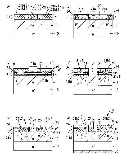
Figs. 4(a)-(f) are diagrams showing a process of manufacturing a UMOSFET in
the embodiment.
Figs. 5(a) and (b) are perspective views of orientations of sides of a trench
in the
embodiment and a modification thereof.
DESCRIPTION OF THE REFERENCE SIGNS
-5-
CA 02669581 2009-05-14
4H-SiC substrate, 11 initial growth layer (base semiconductor layer), 14A
extended kink surface, 14B kink surface, 15A extended terrace surface, 15B
terrace
surface, 16 silicon oxide film, 21 new growth layer, 21a 3C-SiC portion, 21a1
n-type
3C-SiC portion, 21a2 p-type 3C-SiC portion, 21b 4H-SiC portion, 21b1 n-type
5 4H-SiC portion, 21b2 p-type 4H-SiC portion (p-well region), 23 source
region, 24 p+
contact region, 26 gate insulating film, 27 gate electrode, 29 source
electrode, 30 drain
electrode, Ml coating film, M2 carbon cap
BEST MODES FOR CARRYING OUT THE INVENTION
-Formation of Extended Terrace Surface-
10 Figs. 1(a)-(c) are cross-sectional views showing the step of forming an
extended
terrace surface and the step of forming a new growth layer in an embodiment.
In a step shown in Fig. 1(a), an n-type 4H-SiC substrate 10 having a
resistivity
of 0.02 S2cm and a thickness of 400 m as well as using a{ 0001 } surface
offset at
about 8 in a<11-20> direction as a main surface is prepared. Then, an initial
growth
layer (a base semiconductor layer) 11 having a thickness of about 10 m and
including
an n-type dopant having a concentration of about I x 1016 cm 3 is epitaxially
grown on
4H-SiC substrate 10 by using the CVD epitaxial growth method with in-situ
doping.
At this time, a surface portion of initial growth layer 11 includes many steps
having
relatively regular shapes, and a surface of each step includes a kink surface
and a terrace
surface. The terrace surface corresponds to the {0001 } surface and has a
width of
approximately 10 nm. The kink surface corresponds to a{ 11-2n} surface (where
"n"
is any integer) or a(03-38) surface. When a 6H-SiC substrate is used, however,
the
terrace surface corresponds to the {0001 } surface and the kink surface
corresponds to a
(01-14) surface. Many steps having somewhat regular shapes are formed at the
surface of initial growth layer 11. A collection of these steps is called
"bunching
steps." It should be noted that the 6H-SiC substrate may be used instead of
the
4H-SiC substrate. Furthermore, a layer having the bunching steps formed at a
surface
-6-
CA 02669581 2009-05-14
of a silicon carbide substrate itself by heat treatment or the like may be
used as the base
semiconductor layer.
Next, in a step shown in Fig. 1(b), an Si film covering initial growth layer
11 is
deposited, and then is patterned to form a coating film M1 covering a device
formation
region. It should be noted that a region that is not covered with coating film
M1 may
be covered with a resist film. Then, annealing is performed under certain
conditions,
that is, at about 1500 C for about two hours in an atmosphere of Ar. At this
time, in a
region Rtl covered with coating film Ml, an extended terrace surface 15A and
an
extended kink surface 14A created by extending the terrace surface and the
kink surface
of the bunching steps are formed (see a partial enlarged view of region Rtl).
Although
a mechanism for formation of such extended terrace surface has not yet been
fully
elucidated, empirical facts show that steps having extremely extended terrace
surfaces
and kink surfaces are formed by annealing while Si is provided. On the other
hand, in a
region Rt2 that is not covered with the coating film, there are a terrace
surface 15B and
a kink surface 14B that are hardly extended (see a partial enlarged view of
region Rt2).
Extended terrace surface 15A has been extended to have a width of
approximately 0.1-
50 m. Although extended terrace surface 15A has been extended to be ten times
or
more wider than unextended terrace surface 15B, it is not drawn to scale in
the partial
enlarged view in Fig. 1(b) for convenience in illustration.
Although initial growth layer 11 is annealed at 1500 C to form extended
terrace
surface 15A in the present embodiment, the annealing temperature here
preferably has
the following range. The annealing temperature is preferably not higher than
2545 C
in order to suppress sublimation and complete decomposition of SiC. The
annealing
temperature is preferably not higher than 2000 C in order to suppress
sublimation of
SiC into SiCz, Si or SizC to some extent. The annealing temperature is
preferably not
higher than 1800 C in order to sufficiently suppress sublimation of SiC into
SiC2, Si or
Si2C and facilitate control over the surface morphology of initial growth
layer 11. The
annealing temperature is preferably not higher than 1600 C in order to further
improve
-7-
CA 02669581 2009-05-14
the surface morphology of initial growth layer 11.
Although, at the time of annealing, Si is provided to the surface of initial
growth
layer 11 by covering initial growth layer 11 with coating film MI made of Si
in the
present embodiment, other methods can be employed instead of this method. For
example, the other methods include a method of providing Si to the surface of
initial
growth layer 11 by flowing Si-based gas onto the surface of initial growth
layer 11, a
method of providing a liquid including Si to the surface of initial growth
layer 11, a
method of covering initial growth layer 11 with a coating film made of Si02,
or the like,
at the time of annealing.
Next, in a step shown in Fig. 1(c), coating film M1 is removed by using a
mixture of nitric acid and hydrogen fluoride, and then a new growth layer 21
having a
thickness of approximately 1 m is epitaxially grown on initial growth layer
11 by using
the CVD epitaxial growth method with in-situ doping. This new growth layer 21
includes a 3C-SiC portion 21a grown on the region that was covered with the
coating
film, and a 4H-SiC portion 21b grown on the region that was not covered with
coating
film Ml. In Fig. 1(c), although 3C-SiC portion 21a grows in a direction
perpendicular
to extended terrace surface 15A, and therefore 3C-SiC portion 21a and 4H-SiC
portion
21b have an interface inclined with respect to the substrate surface, 3C-SiC
portion 21a
and 4H-SiC portion 21b are depicted as if they did not have the inclined
interface for
convenience sake. A growth mechanism of 3C-SiC having a polytype different
from
4H-SiC on a region having extended terrace surface 15A will be described
hereinafter.
Figs. 2(a) and (b) are diagrams of a growth mechanism in a case where, after
initial growth layer 11 is grown, new growth layer 21 is further epitaxially
grown
without performing annealing with initial growth layer 11 covered with the Si
film. In
other words, Figs. 2(a) and (b) show a growth mechanism in 4H-SiC portion 21b
shown in Fig. 1(c). As shown in Fig. 2(a), an active species (a compound
including Si
and C contributing to epitaxial growth) having reached the upper surface of
narrow
terrace surface 15B of the bunching steps moves on terrace surface 15B and
-8-
CA 02669581 2009-05-14
immediately reaches kink surface 14B. Then, as shown in Fig. 3(b), information
about
the crystal structure of the base layer (initial growth layer 11) is passed on
from kink
surface 14B and a new growth portion made of 4H-SiC starts to be grown (step-
flow
growth). In a case of SiC crystals, since there are many polytypes, good-
quality
homoepitaxial growth is difficult on the { 0001 } surface having little kink
surface.
Therefore, an offset substrate having a main surface offset with respect to
the { 0001 }
surface is generally used.
Figs. 3(a) and (b) are diagrams of a growth mechanism in a case where, after
initial growth layer 11 is grown, annealing is performed with initial growth
layer 11
covered with the Si film, and then new growth layer 21 is epitaxially grown.
In other
words, Figs. 3(a) and (b) show a growth mechanism in 3C-SiC portion 21a shown
in
Fig. 1(c). As shown in Fig. 4(a), even when the active species having reached
extended terrace surface 15A moves on extended terrace surface 15A, it is less
likely to
reach kink surface 14A. This is because terrace surface 15 of the bunching
steps has a
width P1 of approximately 10 nm, whereas extended terrace surface 15A has a
width of
not less than the order of sub- m (not less than 0.1 m and not more than 50
m).
Therefore, as shown in Fig. 4(b), before the active species reaches extended
kink surface
14A, crystal growth starts from the upper surface of extended terrace surface
15A (two-
dimensional nucleation). In this case, the information about the crystal
structure of the
base layer (initial growth layer) is not passed on. Therefore, the
homoepitaxial growth
is less likely to occur and a new growth layer made of 3C-SiC having a
polytype stable
at a low temperature starts to be grown.
-Process of Manufacturing UMOSFET-
Figs. 4(a)-(f) are diagrams showing a process of manufacturing a UMOSFET in
the embodiment. In a step shown in Fig. 4(a), a structure of new growth layer
21 in
the step shown in Fig. 1(c) is described in detail. In Figs. 4(a)-(c),
although 3C-SiC
portion 21a grows in a direction perpendicular to extended terrace surface
15A, and
3C-SiC portion 21a and 4H-SiC portion 21b have an interface inclined with
respect to
-9-
CA 02669581 2009-05-14
the substrate surface, 3C-SiC portion 21a and 4H-SiC portion 21b are depicted
as if
they did not have the inclined interface for convenience sake.
As shown in Fig. 4(a), when new growth layer 21 is epitaxially grown, an n-
type
3C-SiC portion 21a1 and an n-type 4H-SiC portion 21b1 having a thickness of
about
0.2 m and including an n-type dopant having a concentration of about 1 x 10¹⁶
cm"3 are
first epitaxially grown on initial growth layer 11 by using the CVD epitaxial
growth
method with in-situ doping. Next, a p-type 3C-SiC portion 21a2 and a p-type 4H-
SiC
portion 21b2 (p-well region) having a thickness (depth) of about 0.8 m and
including a
p-type dopant having a concentration of about 1 x 10" cm 3 are epitaxially
grown on n-
type 3C-SiC portion 21 al and n-type 4H-SiC portion 21 b 1.
Next, in a step shown in Fig. 4(b), a source region 23 having a thickness
(depth)
of about 0.3 m and including an n-type dopant having a concentration of 1 x
1019 cm 3 is
formed in a region extending over a surface portion of p-type 3C-SiC portion
21a2 and
a surface portion of p-type 4H-SiC portions 21b (p-well regions) on both sides
thereof
in new growth layer 21 by using the ion implantation method. Furthermore, a p+
contact region 24 having a thickness (depth) of about 0.3 m and including a p-
type
dopant having a concentration of 5x 1019 cm 3 is formed in a part of p-type 4H-
SiC
portion 21b2. It should be noted that the temperature of the substrate at the
time of
ion implantation is all 500 C.
Next, in a step shown in Fig. 4(c), a positive-type resist having a thickness
of
2.5-3 m is applied on the entire substrate and heat treatment is performed
under certain
conditions, that is, at 750 C for 15 minutes in an atmosphere of argon to form
a carbon
film having a thickness of 0.8-1 m that covers the substrate. Thereafter, the
carbon
film is patterned to form a carbon cap M2 where a region located on 3C-SiC
portion
21a is open.
Next, in a step shown in Fig. 4(d), thermal annealing is performed under
certain
conditions, that is, at 1700 C for 30-40 minutes in an atmosphere of argon
with 4H-SiC
-10-
CA 02669581 2009-05-14
portion 21b covered with carbon cap M2. As a result, 3C-SiC portion 21a is
sublimed,
whereas 4H-SiC portion 21b having a higher sublimation temperature than that
of
3C-SiC portion 21a is not sublimed and almost all remains. In other words, in
this
step, 3 C-SiC portion 21 a is selectively removed to form a trench Tr having
wall
portions formed of 4H-SiC portions 21b. It should be noted that, even if a
part of
4H-SiC portion 21 a is removed, portions corresponding to sides of trench Tr
have only
to have crystallographic orientations as shown in Fig. 5(a) or 5(b) that will
be described
hereinafter. The appropriate annealing temperature in this annealing step is
preferably
not higher than 2545 C in order to suppress sublimation and decomposition of
4H-SiC
portion 21b. The annealing temperature is preferably not higher than 1600 C in
order
to maintain the surface morphology of 4H-SiC portion 21b in good condition. It
is
seen, however, that the annealing temperature is preferably within a range of
1500-
1900 C in an actual manufacturing process because the appropriate temperature
can
also be adjusted depending on pressure in an atmosphere of Ar or time period.
It should be noted that carbon cap M2 is not necessarily required in order to
sublime 3C-SiC portion 21a. The entire upper surface of the substrate may be
open at
the time of annealing. Sublimation of 4H-SiC portion 21b can, however, be
prevented
more reliably by covering 4H-SiC portion 21b with a mask. Instead of carbon
cap M2,
a mask made of a material having a higher sublimation temperature or a melting
point
than that of SiC such as TaC may be used. In particular, there is an advantage
that
surfaces of source region 23 and p+ contact region 24 are smoothed to have a
surface
roughness Ra of approximately 1-2 nm by annealing with 4H-SiC portion 21b
covered
with the carbon film.
The process of selectively removing cubic 3C-SiC portion 21a with hexagonal
4H-SiC portion 21b remaining is not limited to the above-described sublimation
process
by annealing. For example, only a cubic portion can be selectively removed by
wet
etching, gas etching, RIE, or the like. In the present embodiment, however,
there is an
-11-
CA 02669581 2009-05-14
advantage that 3C-SiC portion 21 a can be selectively removed just by a
relatively
simple process of annealing (heating treatment). In addition, there is also an
advantage
that a sub-trench is not created and etching damage does not occur.
Next, in a step shown in Fig. 4(e), heat treatment is performed under certain
conditions, that is, at 900 C for 30 minutes in an atmosphere of oxygen to
remove
carbon cap M2. Thereafter, a silicon oxide film having a thickness of about 50
nm by
the dry oxidation method in which the temperature of the substrate is
maintained at
about 1200 C and a polysilicon film having a thickness of about 1.2 m are
formed on
the substrate. Then, the silicon oxide film and the polysilicon film are
planarized by
CMP or the like to form a gate insulating film 26 and a gate electrode 27 in
trench Tr.
Next, in a step shown in Fig. 4(f), a drain electrode 30 formed of an Ni film
and
having a thickness of about 0.1 m is formed on a back surface of 4H-SiC
substrate 10
by the vapor deposition method, the sputtering method or the like.
Furthermore, a
source electrode 29 formed of an Ni film and having a thickness of about 0.1
m is
formed on 4H-SiC portion 21b.
Thereafter, heat treatment is performed under certain conditions, that is, at
975 C for two minutes in an atmosphere of argon, and a state where Ni forming
source
electrode 29 and drain electrode 30 contacts silicon carbide forming the base
layer
(source region 23, p+ contact region 24 and p-type 4H-SiC portion 21b2 (p-well
region)) is changed from a Schottky contact to an ohmic contact.
According to the above-described manufacturing process, a UMOSFET that is
an n-channel type vertical transistor and serves as a power device is formed.
Many
transistor cells Us are combined to constitute one UMOSFET although not shown
in
Figs. 4(a)-(f). In each transistor cell U of this UMOSFET, when the UMOSFET is
on,
a current supplied from drain electrode 30 vertically flows from 4H-SiC
substrate 10
through initial growth layer 11 and n-type 4H-SiC portion 21b1 as well as p-
type
4H-SiC portion 21b2 (p-well region) to source region 23. A region of p-type 4H-
SiC
portion 21b2 (p-well region) adjacent to gate insulating film 26 serves as a
channel
-12-
CA 02669581 2009-05-14
region where carriers (electrons in the present embodiment) run. The mobility
of the
electrons in this channel region refers to the channel mobility.
Figs. 5(a) and (b) are perspective views of orientations of the sides of the
trench
in the embodiment and a modification thereof. Cubic 3C-SiC portion 21a is
epitaxially
grown on extended terrace surface 15A almost perpendicularly to extended
terrace
surface 15A. Therefore, the sides of trench Tr formed by selectively removing
3C-SiC
portion 21 a become perpendicular to the { 0001 } surface because extended
terrace
surface 15A corresponds to the {0001 } surface. In other words, the sides of
trench Tr
(4H-SiC portions 21b) can be controlled to have a low-order surface depending
on a
two-dimensional shape (orientation) of mask M1 shown in Fig. 1(b).
In the present embodiment, coating film M1 shown in Fig. 1(b) is configured to
have a rectangular two-dimensional shape whose respective side has a direction
parallel
to a <1-100> direction or a<11-20> direction of initial growth layer 11 (base
semiconductor layer). As a result, as shown in Fig. 5(a), portions
corresponding to the
sides of trench Tr in 4H-SiC portion 21b have a{ 11-201 surface or a{ 1-100}
surface.
In other words, the channel region of the UMOSFET is formed along the { 11-20}
surface or the { 1-100} surface, and the carriers (electrons in the present
embodiment)
run along the low-order surface. Therefore, a UMOSFET having high channel
mobility
is obtained.
In the modification, coating film Ml shown in Fig. 1(b) is configured to have
a
hexagonal two-dimensional shape whose respective side has a direction parallel
to the
<1-100> direction of initial growth layer 11 (base semiconductor layer). As a
result,
as shown in Fig. 5(b), the portions corresponding to the sides of trench Tr in
4H-SiC
portion 21b have the { 1-100} surface. In other words, the channel region of
the
UMOSFET is formed along the { 1-100} surface, and the carriers (electrons in
the
present embodiment) run along the low-order surface. Therefore, a UMOSFET
having
high channel mobility is also obtained according to the modification.
According to the embodiment and the modification described above, in a case
- 13 -
CA 02669581 2009-05-14
where the base senvconductor layer (initial growth layer 11) having a main
surface
inclined at not smaller than 2 in the <1-100> direction or the <1 1-20>
direction with
respect to the {0001 } surface is used, the carriers run along the { 11-20}
surface or the
{ 1-100} surface that is the low-order surface, if coating film Ml has a
polygonal two-
dimensional shape where at least one side is orthogonal to the direction of
inclination.
It should be noted that, in the present embodiment, a diode such as a Schottky
diode or a pn diode is formed in 4H-SiC portion 21b of new growth layer 21,
although
illustration is not given. A diode, however, does not necessarily have to be
provided
on the same substrate as a transistor.
(Other Embodiments)
A silicon carbide semiconductor device according to the present invention is
not
limited to the devices described in the first and second embodiments, but can
have any
variations in terms of a structure, a dimension, a dopant concentration, or
the like of
each portion as long as the device can produce the effects of the invention.
A silicon carbide substrate that is one silicon carbide semiconductor
substrate in
the present invention is not limited to a 4H-SiC substrate, but may be a
hexagonal SiC
substrate having a polytype different from a 4H polytype, such as a 6H-SiC
substrate.
Although an example in which a silicon carbide semiconductor device according
to the present invention is applied to a UMOSFET have been described in the
embodiment, the silicon carbide semiconductor device according to the present
invention is also applicable to a device where a gate insulating film is an
insulating film
different from a silicon oxide film, for example a silicon nitride film, a
silicon oxynitride
film, other dielectric films of various types, or the like. In addition, the
silicon carbide
semiconductor device according to the present invention is also applicable to
an IGBT
or the like.
INDUSTRIAL APPLICABILITY
A silicon carbide semiconductor device according to the present invention can
be
employed in a UMOSFET, an IGBT or the like used as a power device or a high-
- 14-
CA 02669581 2009-05-14
frequency device.
-15-