Note : Les descriptions sont présentées dans la langue officielle dans laquelle elles ont été soumises.
CA 02671388 2009-06-01
WO 2008/071945 1 PCT/GB2007/004748
AN ANTENNA ARRANGEMENT
This invention relates to an antenna arrangement for operation at frequencies
in excess
of 200 MHz, and to a mobile terminal including the antenna arrangement.
GB-A-2292638, GB-A-2309592 and GB-A-2311675 all disclose examples of
dielectrically-loaded antennas having certain common features. Each antenna
includes
a solid cylindrical ceramic core of high relative dielectric constant, a
coaxial feeder
passing through the core on its axis to a termination at a distal end, a
conductive sleeve
plated on a proximal portion of the core, and a plurality of elongate helical
conductor
elements plated on the cylindrical surface of the core and extending between
radial
connections with the feeder termination on the distal end face and the rim of
the sleeve.
The combination of the conductive sleeve and an outer sleeve of the coaxial
feeder
form a quarterwave balun which creates an at least approximately balanced
condition at
the connection between the feeder and the radial connections at the distal end
of the
core.
GB-A-2292638 discloses a quadrifilar backfire antenna having four elongate
helical
elements formed as two pairs, the electrical length of the elements of one
pair being
different from the electrical length of the elements of the other pair. This
structure has
the effect of creating orthogonally phased currents at an operating frequency
of, for
example, 1575MHz with the result that the antenna has a largely omni-
directional
radiation pattern for circularly polarised signals such as those transmitted
by the
satellites in the GPS (Global Positioning System) satellite constellation.
GB-A-2309592 discloses an antenna having a single pair of diametrically
opposed
helical elements forming a twisted loop yielding a radiation pattern which is
omni-
directional with the exception of nulls centred on a null axis extending
perpendicularly
to the cylindrical axis of the antenna. This antenna is particularly suitable
for use in a
portable telephone, and can be dimensioned to produce loop resonances at
fiequencies
respectively within the European GSM band (890 to 960 MHz) and the DCS band
CA 02671388 2009-06-01
WO 2008/071945 2 PCT/GB2007/004748
(1710 to 1880 MHz), for example. Other relevant bands include the American
AMPS
(842 to 894 MHz) and PCN (1850 to 1990 MHz) bands.
GB-A-2311675 discloses the use of an antenna having the same general structure
as
that disclosed in GB-A-2202638 in a dual service system such as a combined GPS
and
mobile telephone system, the antenna being used for GPS reception when
resonant in a
quadrifilar (circularly polarised) mode and for telephone signals when
resonant in a
single-ended (linearly polarised) mode.
It is has been found by the applicant that for most applications the core of
an antenna
such as those described above having a diameter of 10mm provides the required
efficiency. In particular, antennas suitable for L-band GPS reception at
1575MHz have
a diameter of about 10mm and the longitudinally extending antenna elements
have an
average longitudinal extent of about 12mm. At 1575MHz, the length of the
conductive
sleeve is typically in the region of 5mm. The diameter of the coaxial feed
structure in
the bore is in the region of 2mm. Other dielectrically-loaded antennas
disclosed by the
applicant have similar dimensions, and for most applications have a diameter
of about
10mm.
The above-noted antennas are particularly suitable for use in small hand-held
devices
not only due to their small size, but also because they do not experience
appreciable
detuning when placed close to objects such as the human body. Hitherto,
antennas
having a diameter of 10mm have been small enough to fit in most mobile
devices. As
with other types of portable devices, one of the main design criteria is
miniaturisation.
Thus, mobile device manufacturers envisage requiring dielectrically-loaded
antennas
having widths of less than 10 mm. However, reducing the size of a
dielectrically
loaded antenna such as those described above significantly reduces the
efficiency of the
antenna. This is because, to a first approximation, efficiency is proportional
to
radiation resistance which, in turn, is inversely proportional to the square
of the
diameter.
It is an object of the present invention to mitigate or avoid a reduction in
antenna
efficiency in mobile devices of reduced dimensions.
CA 02671388 2009-06-01
WO 2008/071945 3 PCT/GB2007/004748
According to a first aspect of the present invention, an antenna arrangement
comprises
at least two antennas each resonant at a common operating frequency, and a
circuit
arranged to combine output signals from each of the said antennas at the said
frequency
to provide a combined signal output, wherein each antenna comprises: an
electrically
insulative core of solid material having a relative dielectric constant
greater than 5, and
a three-dimensional antenna element structure including at least a pair of
elongate
conductive antenna elements disposed on or adjacent a surface of the core.
Such an arrangement has a larger effective aperture for electromagnetic
radiation when
compared with an arrangement having a single antenna of similar dimensions. As
a
result, efficiency is improved to the extent that an antenna arrangement in
accordance
with the invention may use antennas having smaller diameters than
corresponding
single antenna arrangements.
Preferably the combining circuit comprises an output node and a plurality of
arms, each
arm being connected between a respective antenna and the output node.
Typically,
each antenna comprises a feed connection coupled to respective first ends of
the arms,
the other ends of the arms constituting the output node. In the preferred
embodiment of
the invention, the combining circuit is configured such that each feed
connection is
isolated from each other feed connection at the operating frequency, this
typically being
achieved by arranging for each arm to comprise a phase-shifting and impedance
transforming element for effecting a 90 phase-shift between the ends of the
arm at the
operating frequency and for stepping up the impedance presented by the
respective
antenna and any interposed network at the feed connection of the antenna, such
phase-
shifting and impedance-transforming elements being interconnected at the feed
connections by a cancelling resistance between each pair of elements. The
value of the
resistance is preferably chosen such that, at each feed connection of a pair
of feed
connections, a voltage component present at that feed connection as a result
of a signal
at the other feed comlection of the pair being transmitted through the two
arms via the
output node is equal in magnitude and opposite in phase to another voltage
component
transmitted from the source feed corulection via the cancelling resistance. It
follows
that the resulting voltage, being the sum of the two components, is
substantially zero.
Consequently, the antenna feed connections are isolated from each other. The
phase-
shifting and impedance-transforming elements may be quarterwave transmission
line
CA 02671388 2009-06-01
WO 2008/071945 4 PCT/GB2007/004748
sections or lumped components. In the case of them being quarterwave
transmission
line sections, they are preferably microstrip lines which, in the case of an
arrangement
having two antemlas, typically have a characteristic impedance of about F2 x
the
output impedance of the combining circuit. Thus, if the output impedance is 50
oluns,
the characteristic impedance of the transmission line sections is about 71
ohms.
In the preferred embodiment, the arrangement comprises two antennas which are
eacli
connected by a microstrip transmission line to the output node. A single
resistor is
connected between the feed connections of the antennas.
The core of each antenna is preferably a cylinder having a length of coaxial
feeder
passing along its axis and terminating at a distal end of the core. The
coaxial feeder has
an inner conductor and an outer shield conductor wllich are separated byan
insulative
sheath. A conductive sleeve is plated around a proximal end of the core and is
coupled
to the shield conductor of the coaxial feeder at the proximal end of the core.
The
elongate conductive antenna elements are preferably helical tracks which
extend from a
connection with the coaxial feeder at the distal end of the core, to a
connection with the
rim of the conductive sleeve on the cylindrical surface of the core. The
conductive
sleeve acts in combination with the feeder as a balun to promote a
substantially
balanced condition at the connection between the coaxial feeder and the
helical
elements.
The antennas generally share substantially the same dimensions and are
preferably
identical. The antennas of the arrangement are preferably positioned such that
the axis
of each antenna is parallel to the axis of the other antenna and such that
first and
second end faces of the antennas lie substantially in common first and second
planes.
The axes of the antennas are typically closer together than half a wavelength
at the
operating frequency (approximately 9.5cm at 1575MHz) in order substantially to
avoid
problems with diffraction patterns. Advantageously, the cylindrical surfaces
of the
antennas are at least 0.09, apart to avoid excessive coupling between the
antennas, k
being the wavelength in air at the operating frequency. This range of inter-
antenna
CA 02671388 2009-06-01
WO 2008/071945 5 PCT/GB2007/004748
spacings lends the arrangement to a variety of devices, especially handheld
devices
such as cellphones .
It is particularly advantageous that the arrangement comprises a pair of
substantially
identical helical antennas eacli having a respective central axis, with the
two axes
parallel and spaced apart, the two antennas further having the same axial
position as
eacll other, and the rotational positions of the antennas about their
respective axes
differing by 180 . This has the effect of causing charge summation in the
space
between the antennas, with benefits to the radiation pattern of the
arrangement as a
whole.
This may be understood more clearly by considering the effect of having two
antennas
with the same orientation placed close together and driven at their feed
connections by
signals having the same phase. As the two antennas are moved progressively
closer to
eacll other, the first observable effect is that the radiation patterns of the
individual
antennas are distorted. In the case of two antennas for circularly polarised
radiation,
the cause of this effect can be visualised by considering two rotating dipoles
in the
near-field. If, at an instant that the dipoles are aligned along a line
connecting the two
antennas, then, providing the antennas are similar and similarly oriented, the
electric
charges in the space between the antennas will tend to cancel, reducing the
overall
charge concentration in the central region so that the combined charge pattern
at the
given instant resembles a single dipole across the pair of antennas. The
consequence of
this is that the combined circular polarisation pattern is impaired. This
impairment can
be mitigated by orienting the antemlas differently, as described above. Now,
with the
new orientations, the two charge dipoles at a given instant are in opposition
when
aligned alone the line of connection between the antennas. It is, therefore,
possible,
using this feature; to place the antennas closer together than would otherwise
be
practicable whilst maintaining the required performance in terms of radiation
pattern.
Since, for a circularly polarised wave incident upon such an antenna
arrangement in the
direction of the axes, the respective signals fed from the antennas differ in
phase by
180 , the preferred arrangement has a halfwave delay line connected between
the feed
connection of one of the antennas and its associated quarterwave transmission
line of
the combining circuit.
CA 02671388 2009-06-01
WO 2008/071945 6 PCT/GB2007/004748
According to a further aspect, the present invention provides a mobile
terminal
comprising the above antenna arrangement.
According to a further aspect of the invention, a mobile terminal comprises
two
antennas for operation at frequencies in excess of 200MHz, the antennas each
comprising an electrically insulative core of solid material having a
dielectric constant
greater than 5, a three-dimensional antenna element structure having at least
a pair of
anterma elements, and a feed connection, wherein the mobile terminal further
comprises
a circuit arrangement which couples the feed connections to a common output
node,
and isolates each feed connection from the other feed connection, thereby to
provide a
combined signal output.
According to yet a further aspect, the invention provides an antenna assembly
for a
handheld radio signal receiver, comprising: at least two dielectrically loaded
antennas
each resonant at a common operating frequency and each comprising an
insulative core
of a solid dielectric material which has a relative dielectric constant
greater than 5 and
which occupies the major part of the volume and defined by the outer surfaces
of the
core, a three dimensional antenna element structure including at least a pair
of elongate
conductive antenna elements disposed on or adjacent an outer surface of the
core, and
an output connection coupled to the antenna element structure; and a signal
combiner
coupled to the respective output connections of the antennas and arranged to
combine
signals present at the output connections at the said common operating
frequency to
provide a combined signal output; the antennas being mounted in a spaced-apart
relationship in the assembly.
According to yet a further aspect, the invention provides a portable clamshell
terminal
comprising a body portion housing a microphone and having an inner face, a
cover
portion housing an earphone, and, associated with an edge of the body portion,
a hinge
arrangement connecting the cover portion to the body portion to allow the
cover portion
to be pivoted between an open position in which the inner face is exposed and
a closed
position in which it covers the inner face, the terminal further comprising at
least two
dielectrically-loaded antennas each having a central axis, and a combiner
circuit for
combining signals received by the two antennas, the antennas being mounted in
the
CA 02671388 2009-06-01
7 PCT/GB2007/004748
WO 2008/071945
body portion in the region of the hinge arrangement with their central axes
parallel to
each other and generally parallel to the inner face of the body portion, the
antennas
being in a side-by-side configuration in which they are spaced apart in the
direction of
the hinge axis.
Typically, the spacing between the antennas, at their closest points, is
between 10mm
and 401nm, to suit the styling of the terminal.
Preferably, the hinge arrangement comprises two axially spaced-apart hinge
parts
associated with respective sides of the body portion and having a coinmon
hinge axis,
and the antenna arrangement comprises a pair of antennas located between the
hinge
parts.
According to yet a further aspect, the present invention provides a portable
clamshell
terminal having a body portion and a cover portion hinged to the body portion,
and a
pair of dielectrically loaded helical antennas each resonant at a common
operating
frequency and each having a respective axis of symmetry, wherein the antennas
are
mounted in the region of the hinge axis and in a spaced-apart side-by-side
configuration
with their axes parallel.
The antenna arrangement described above can serve for signal transmission as
well as
signal reception. Accordingly, the invention also provides an antenna
arrangement for
a portable terminal, comprising: at least two antennas each resonant at a
coinmon
operating frequency, and a circuit arranged to split an input signal into
substantially
identical split signals and to feed the split signals to each of the antennas,
wherein each
antenna comprises: an electrically insulative core of a solid material having
a relative
dielectric constant greater than 5, and a three-dimensional antenna element
structure
including at least a pair of elongate conductive antenna elements disposed on
or
adjacent a surface of the core.
The invention will now be described by way of example with reference to the
drawings
in which:
CA 02671388 2009-06-01
WO 2008/071945 8 PCT/GB2007/004748
Figures 1 A to 1 C are diagrams of a part of a mobile terminal incorporating a
first
antenna arrangement in accordance with the present invention;
Figure 2 is a perspective view of an antenna which forms part of the antenna
arrangement shown in Figure 1, viewed from above and one side;
Figure 3 is another perspective view of the antenna shown in Figure 2, viewed
from
below and one side;
Figure 4 is a longitudinal cross-section of a feed structure of the anteima of
Figures 2
and 3;
Figure 5 is a schematic circuit diagram of the feed structure and antenna of
Figures 3
and 4;
Figure 6 is a schematic diagram of a combiner circuit of the antenna
arrangeinent of
Figures 1 A to 1 C;
Figure 7 is a diagrammatic representation of the radiation patterns of the
antennas
shown in Figure 1A;
Figures 8A to 8C are diagrams of part of a mobile terminal including an
alternative
embodiment of the present invention; and
Figure 9 is a perspective view of a portable tenninal in accordance with the
invention.
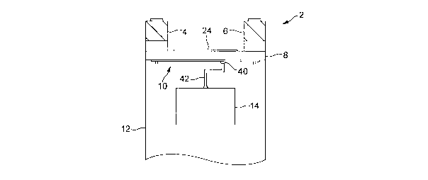
Referring to Figures 1 A to IC, an antenna arrangement 2 in accordance with
the
invention includes two antennas 4, 6 which are mounted on an antenna-mounting
printed circuit board (PCB) 8 (or other suitable board). The PCB 8 is
elongate, and
anteimas 4, 6 are mounted at either end. A combining circuit 10 is located on
the
underside of the PCB 8, that is to say, the side opposing that on which the
antennas are
mounted.. The PCB 8 is mounted perpendicularly to a device PCB 12. A receiver
14 is
mounted on the device PCB 12. The antennas are coupled to the combining
circuit 10
CA 02671388 2009-06-01
9
WO 2008/071945 PCT/GB2007/004748
which is coupled to receiver 14. The antenna arrangement will be described in
more
detail below.
The antennas 4, 6 are identical and are quadrifilar dielectrically-loaded
antennas.
Referring to Figures 2 and 3, the antenna 60 includes a cylindrical core 62 of
electrically insulative material having a dielectric constant greater than 5.
The antenna
comprises an antenna element structure with four axially coextensive helical
tracks
60A, 60B, 60C, 60D plated or otherwise metallised on the cylindrical outer
surface of
the cylindrical ceramic core 62. The core has an axial passage in the forrn of
a bore
(not shown) extending through the core 62 from a distal end face 62D to a
proximal end
face 62P. Both of these faces are planar faces perpendicular to the central
axis of the
core. They are oppositely directed, in that one is directed distally and the
other is
directed proximally. Housed within the bore 62B is a coaxial feeder structure.
As
shown in Figure 4, the feeder structure includes a coaxial transmission line
70 with a
conductive tubular outer shield 72, a first tubular insulating layer 74, and
an elongate
inner conductor 76 which is insulated from the shield by layer the 74. In this
case the
insulating layer 74 is a first air gap. The shield 72 has outwardly projecting
and
integrally formed spring tangs 72T or spacers which space the shield from the
walls of
the bore. A second tubular air gap therefore exists between the shield 72 and
the wall
of the bore.
At the lower, proximal end of the feeder structure, the inner conductor 76 is
centrally
located within the shield 72 by an insulative bush 78B. The transmission line
70 has a
predetermined characteristic impedance, here 50 ohms, and passes through the
antenna
core 62 for coupling distal ends of the antenna elements 60A to 60D to radio
frequency
(RF) circuitry of equipment to which the antenna is to be connected. The
couplings
between the antenna elements 60A - 60D and the feeder are made via a laminate
board
(PCB) 80 and radial conductors associated with the helical tracks 60A to 60D,
these
conductors being formed as radial tracks 60AR, 60BR, 60CR, 60DR plated on the
distal end face 62D of the core 62. Each radial track extends from a distal
end of the
respective helical track to a location adjacent the end of the bore 62B The
structure of
the matching assembly and its connection to the distal end of the transmission
line 70 is
described below. At the proximal end of the transmission line 70, the inner
conductor
CA 02671388 2009-06-01
WO 2008/071945 10 PCT/GB2007/004748
76 has a proximal portion 76P (see Figure 3) which projects as a pin from the
proximal
face 62P of the core 62 for connection to the equipment circuitry. Similarly,
integral
lugs 72F on the proximal end of the shield 72 project beyond the core proximal
face
62P for making a connection with the equipment circuitry ground.
A conductive sleeve 64 is plated on a proximal end of the core 62. The
proximal end
face 62P of the core is plated with a conductor 68 which connects the coaxial
outer
shield 72 on the proximal end' face 62P of the core to the sleeve 64. The
helical antenna
elements 60A - 60D, extend between the connection with the coaxial feed line
at the
distal end of the core 62D, and a connection with a rim 66 of the conductive
sleeve 64.
The conductive sleeve 64 and the outer sleeve of the coaxial feed act as an
balun
promoting a substantially balanced condition at the connection between the
helical
elements 60A - 60D and the coaxial transmission line.
The four helical antenna elenients 60A - 60D are of different lengths, two of
the
elements 60B, 60D being longer than the other two 60A, 60C as a result of the
rim 66
of the sleeve 64 being of varying distance from the proximal end face 62P of
the core.
Thus, where the shorter antenna elements 60A, 60C are connected to the sleeve
64, the
rim 66 is a little further from proximal face 62P than where the longer
antenna elements
10B and l OD are connected to the sleeve 20.
The differing lengths of the antenna elements 60A to 60D result in phase
differences
between currents in the longer elements 60B, 60D and those in the shorter
elements
60A, 60C respectively when the antenna operates in a mode of resonance in
which the
antenna is sensitive to circularly polarised signals. Operation of quadrifilar
dielectrically loaded antennas having a balun sleeve is described in more
detail in GB-
A- 2292638 and GB-A-2310543A.
The planar laminate board 80 of the feeder structure is connected to a distal
end of the
line 70. The laminate board or printed circuit board (PCB) 801ies flat against
the distal
end face of the core 62D, in face-to-face contact. The largest dimension of
the PCB 80
is smaller than the diameter of the core 62 so that the PCB 80 is fully within
the
periphery of the distal end face 62D of the core 62.
CA 02671388 2009-06-01
WO 2008/071945 11 PCT/GB2007/004748
The PCB 80 is in the form of a disc centrally located on the distal face 62D
of the core.
Its diameter is such that it overlies the inner ends of the radial tracks
60AR, 60BR,
60CR, 60DR and their respective part-annular interconnections 60AB, 60CD. The
PCB 80 has a substantially central hole 82 which receives the inner conductor
76 of the
coaxial feeder structure. Three off-centre holes 84 receive distal lugs 72G of
the shield
72. Lugs 72G are bent or "jogged" to assist in locating the PCB 80 with
respect to the
coaxial feeder structure.
The PCB 80 is a multiple layer laminate board in that it has a plurality of
insulative
layers and a plurality of conductive layers. In this embodiment, the laminate
board is
arranged to provide a capacitance and an inductance between the coaxial line
70 and
the antenna elements 60A, 60B, 60C, 60D, a shown in Figure 5. Here, the
antenna
elements are represented by conductor 90, and the coaxial feed is represented
by
conductor 92. Further details of this arrangement are provided in co-pending
International Patent Application No. PCT/GB2006/002257.
Referring again to Figures 1A to 1C in conjunction with Figure 3, the antennas
4, 6 are
mounted by their proximal end faces 62P to the antenna-mounting PCB 8. The
lugs
72F and proximal inner conductor 76P pass through holes formed in PCB 8 and
protrude from the underside of the PCB 8. The inner conductor 76P of antenna 4
is
connected to a first circuit node 26 and the inner conductor 76P of antenna 6
is
connected to a second circuit node 28. First node 26 is connected to a third
circuit node
by a length of microstrip transmission line 32 which has a length equal to one
half
wavelength at the operating frequency of the device. For example, L-band GPS
signals
25 have a frequency of 1.575GHz and a wavelength of approximately 19cm. The
length
of the transmission line 32 is 9.5cm divided by the square root of the
effective relative
dielectric constant, which is dependent on the dimensions of the microstrip
line and the
material of the substrate carrying it. A resistor 34 is connected between the
third node
30 and second node 28. The resistor has a value of twice the source impedance
of each
30 antenna, and in this case has a value of 100 ohms. The circuit also
comprises two
quarter wavelength microstrip transmission lines 36, 38. One end of each line
36, 38 is
connected to a respective one of the second and third nodes 28, 30. The other
end of
each transmission line is connected to an output node 40. The transmission
lines 36, 38
CA 02671388 2009-06-01
WO 2008/071945 12 PCT/GB2007/004748
have a characteristic impedance of -\r2- times the output impedance of the
circuit 10,
and in the present case the characteristic impedance of each of the
transmission lines is
typically 71 ohms.
The lugs 72F are connected to conductive track portions 16, 18 which are also
connected, respectively, to through-holes 20, 22 formed on the antenna-
mounting PCB
8. These through-holes are plated on their inner surfaces and are hereinafter
referred to
as vias. A conductor 24, formed on an upper surface of the PCB 8, is also
connected to
the vias 20, 22. This conductor covers an area substantially the same as the
circuit 10
and is the ground-plane conductor for the microstrip transmission lines 32,
36, 38.
The output node 40 is connected to a conductive track 42 using solder which,
in turn, is
connected to the radio signal receiving circuit 14. The conductive tracks 16,
18 are
further connected to vias 44, 46 in the device PCB 12.. The vias 44, 46 are
connected
to a ground-plane 48 of the device PCB 12.
Referring to Figure 6, the microstrip transmission lines of the Wilkinson
combiner are
shown as quarter-wave transformers 50, 52 and the resistor connected between
the third
node 30 and second node 28 is shown as R. The antenna element structure of
each
antenna is shown respectively as 54 and 56. The phase-compensating delay line
is
shown as a half-wave transformer 58.
As noted above in relation to Figure 2, two of the helical antenna elements
60B, 60D
are longer than the other two helical elements 60A, 60C. This length
difference is
important to the antenna's ability to receive circularly polarised signals. In
use, when a
radio signal is received by the antenna 60, a dipole is generated across the
core 62
between opposing antenna elements (e.g. 60B, 60D). This is a rotating dipole,
the
orientation of which, at any given instant, depends not only on time, but also
on the
orientation of the antenna. For a given received radio signal received by the
antenna
arrangement containing this antenna (as shown in Figures 1 A- 1 C), rotation
of the
antenna by 180 degrees about its longitudinal axis will cause the dipole to be
reversed
in polarity.
CA 02671388 2009-06-01
WO 2008/071945 13 PCT/GB2007/004748
Referring again to Figure lA in conjunction with Figures 2 and 3, antenna 6 is
oriented
such that its antenna elements are at 180 degrees with respect to the
corresponding
antenna elements of antenna 4. In particular, antenna 4 is oriented such that
its antenna
elements 60C and 60C are directed towards antenna 6, and antenna 6 is oriented
such
that its antenna elements 60C and 60D are directed towards antenna 4. In this
maimer,
when a radio signal is incident upon the arrangement 2, the dipoles generated
in each
antenna 4, 6, are polarised, at any given instant, oppositely to the dipole
generated in
the other antenna as shown in Figure 7. Accordingly, the dipoles mirror each
other and,
therefore, charge cancellation in the space between the antennas is avoided,
as
described hereinbefore. This results in a combined radiation pattern which is
omni-
directional and which is not reduced between the antennas. It will be
understood by
those skilled in the art that antennas obey the law of reciprocity. Thus the
phrase
"radiation pattern" is used in the sense understood by those skilled in the
art, that is to
mean a pattern which does not necessarily represent radiated energy as it
would if the
antenna is connected to a transmitter, and to mean, therefore, a pattern which
represents
the antenna's ability to both collect and radiate electromagnetic radiation
energy.
Owing to this arrangement, signals generated by the antennas 4, 6 in response
to a
given received radio signal are 180 degrees out-of-phase. The half-wave
transmission
line 32 compensates for this by delaying the signal generated by one of the
antennas
(antenna 4) by one half wavelength.
Referring to Figures 8A to 8C, an alternative antenna arrangement 100 in
accordance
with the invention is shown. Features which it has in common with the
arrangement
shown in Figures lA to 1C are indicated with like reference numerals. In this
embodiment, the combining circuit 10 is formed on the device PCB 12 rather
than on
the antenna-mounting PCB 8. Each antenna 4, 6 has an alternative feed
connection
arrangement in which the coaxial feed line extends beyond the surface of the
proximal
end 62P of the antenna. The extended coaxial feed line comprises a proximal
inner
conductor 102 and a proximal outer conductor 104. The inner conductor 102 and
the
outer conductor 104 are separated by an insulator. The proximal ends of the
outer
conductor 104 and the insulator lie flush with each other at a short distance
from the
end face 62P. The inner conductor 102 extends beyond these parts of the feed
connection allowing connection to external circuitry. The inner conductors 102
and
CA 02671388 2009-06-01
WO 2008/071945 14 PCT/GB2007/004748
outer conductors 104 are located in through-holes in the antenna-mounting PCB
8. The
outer conductors 104 are connected to vias 106 in the device PCB 12 which are
connected to a ground plane 108 on the underside of device PCB 12. The inner
conductors 102 are coupled to conductor tracks formed on an upper surface,
that is to
say, the surface of the device PCB 12 opposing that on which the ground plane
is
formed. The combining circuit 10 is the same as that described above in
relation to
Figures 1 A to 1 C. The antennas 4, 6 are oriented as described above with
reference to
Figures 1 A to 1 C.
With reference to Figures lA to 1C and 8A to 8C, the antennas have been
described as
being rotationally oriented at 180 degrees with respect to each other about
their
respective axes. In an alternative arrangement, the antennas 4, 6 are located
so that the
top face 62D of one antenna 4 is offset by a half wavelength above or below
the top
face 62D of the other anterina 6. In this arrangement, the antennas 4, 6 are
not
differently rotationally oriented. In other words, their rotational
orientation in the
mobile terminal is the same. In this arrangement, the diploes generated by
each
antenna are also oppositely polarised for any given received radio signal at a
given
axial height in the terminal. As noted above, this avoids charge cancellation
between
the antennas.
Referring to Figure 9, to give an example of a mobile terminal incorporating
the
antenna arrangement described above with reference to Figures 1 to 7, a
clamshell
terminal 110, such as a mobile phone, is shown in an open configuration. The
clamshell terminal 110 comprises a body section 112 and a cover section 114
which
are interim connected by a pair of coaxial hinge parts 116, 118. The cover
section 114
comprises an inner face (not shown) and typically houses a display. The body
section
112 comprises an inner face' (also not shown), and typically houses a keypad.
The
hinge parts 116, 118 are arranged to allow the cover section 114 to move
between a
closed configuration (not shown) on the body section 112 and the open
configuration.
An antenna housing 120 is formed integrally with the body section 112 as an
upper
edge portion of the body section and is positioned between the hinge parts
116, 118.
The two dielectrically-loaded cylindrical antennas 4, 6 are mounted at either
end of the
housing 120. The antennas 4, 6 are spaced apart by at least 0.05k apart, and
in this case
CA 02671388 2009-06-01
WO 2008/071945 15 PCT/GB2007/004748
are about around 20mm apart. Their distal ends are directed outwardly from the
upper
edge of the body section 112 so as to be directed generally skywards when the
mobile
phone is in use or is held with the inner face of the body section 112
upright. In
particular, the antennas 4, 6 are oriented with their axes substantially
parallel to the
inner face of the body section 114 and defining a plane which, in addition to
being
parallel to the inner face, extends behind the inner face. The axes are spaced
apart in a
direction normal to the axes and are arranged symmetrically about a centre
line of the
body section 114.