Note : Les descriptions sont présentées dans la langue officielle dans laquelle elles ont été soumises.
CA 02673705 2009-07-22
PATENT APPLICATION
INTERFACE-INFUSED NANOTUBE INTERCONNECT
INVENTOR: Keith A. Slinker
Vasiliki Z. Poenitzscli
ATTORNEY DOCKET: 0408RF.045953 (T4-01054)
Field of the Invention
[0001] The present invention relates to a method of fabricating arrays and
devices that
incorporate carbon nanotubes.
Background of the Invention
[0002] Carbon nanotubes (CNTs) have gained( much interest due to the very
unique and
desirable properties exhibited by the materials and by devices that are
prepared with CNTs.
Carbon nanotubes are very small tube-shaped structures each having the
structure of a graphite
sheet rolled into a tube. Carbon nanotubes exhibit excellent mechanical
properties, such as for
example, a high Young's modulus, a high elastic modulus, and low density. In
addition, CNTs
also demonstrate excellent electrical, thermal, electromechanical and
absorption properties.
Carbon nanotubes display electronic metallic properties or semiconductor
properties according to
different ways in which the graphite sheet is rolled. Due to these and other
properties, it has
been suggested that carbon nanotubes may play an important role in a variety
of different fields,
such as for example, microscopic electronics, materials science, biology and
chemistry. One
-1-
CA 02673705 2015-12-14
particular use that has been suggested is as field emission cathodes for the
replacement of
thermionic cathodes used in microwave tubes.
100031 Carbon nanotubes are also highly desirable due to their ability to
form self-assembling
linear, forest-like arrays. CNT arrays have been shown to have high thermal
and electrical
conductivity, extremely low optical reflectivity, excellent emission
properties, and to be
compliant yet strong. Thus they have been suggested for applications such as
field emission
devices, conformable electrical interconnects, and mechanically resilient
thermal interconnects.
However, these CNT arrays generally show poor adhesion and poor conductivity
to the
substrates they are synthesized on as well as low self-integrity, thereby
limiting their potential
for use in forming matrices and the fabrication of microelectronic and other
devices.
Summary
100041 In one aspect, a method is provided for the preparation of
vertically aligned carbon
nanotube arrays that incorporate a coating on at least one end of the array. A
substrate suitable
for supporting the growth of carbon nanotubes is provided and a plurality of
carbon nanotubes
are synthesized on a surface of the substrate. The carbon nanotubes include a
first end and a
second end, wherein the first end is attached to the substrate and wherein
said plurality of carbon
nanotubes forms a forest of substantially vertically aligned nanotubes. A
coating is then
deposited on the second end of the carbon nanotubes.
100051 In certain embodiments, the method further includes the steps of
removing the
substrate from the first end of the carbon nanotubes and depositing a second
coating on the first
end of the carbon nanotubes. The coating layer can be selected from a variety
of materials,
including metal, composites, alloys, and polymers.
-2-
CA 02673705 2016-09-26
100061 In another aspect, a carbon nanotube array is provided that
incorporates a coating
on at least one end of the carbon nanotube array, wherein the coating is
partially infused into
te carbon nanotube array.
[0006A] In a broad aspect, the invention pertains to a method of forming a
carbon
nanotube array, comprising providing a substrate suitable for supporting the
growth of a plurality
of carbon nanotubes, and depositing the plurality of carbon nanotubes on a
surface of the
substrate. The carbon nanotubes have a first end and a second end, and the
first end is attached
to the substrate, and the plurality of carbon nanotubes forms a forest of
aligned nanotubes. A
first coating is deposited on the second end of the carbon nanotubes, the
first coating partially
infusing along a length of the carbon nanotubes from the second end. The first
end is removed
from the substrate, and a second coating is deposited on the first end of the
carbon nanotubes,
the second coating partially infusing along the length of the carbon nanotubes
from the first end.
A first object is attached to at least one of the first and second coatings to
form a thermal
interconnect.
10006B1 In a further aspect, the invention provides a carbon nanotube
array, comprising
a plurality of vertically aligned carbon nanotubes, the nanotubes having a
first and a second end,
and a length extending between the first and second ends. A first coating is
infused to and
bonds the first ends of the carbon nanotubes together. The first coating only
partially infuses
along the lengths of the carbon nanotubes from the first end. A second coating
is infused to and
bonds the second ends of the carbon nanotubes together. The second coating
only partially
- 3 -
CA 02673705 2016-09-26
infuses along the length of the carbon nanotubes from the second end. There is
an exposed
= portion of the lengths of the carbon nanotubes between the first and
second coatings and free of
infusion of the first and second coatings, so as to remain compliant under
compression.
10006C1
In a still further aspect, the invention embodies a carbon nanotube array,
comprising a plurality of vertically aligned carbon nanotubes. The nanotubes
have a first and
a second end, and a second end cap layer is coupled to the first end of the
plurality vertically
aligned carbon nanotubes. The second end cap layer partially infuses the
plurality of vertically
aligned carbon nanotubes, and the second end cap layer is fused to a second
object. A first end
cap layer is coupled to the second end of the plurality of vertically aligned
carbon nanotubes,
wherein the first end cap layer partially infuses the plurality of vertically
aligned carbon
nanotubes and the first end cap layer is fused to a first object, so that the
first and second objects
are in thermal communication through the plurality of vertically aligned
carbon nanotubes.
- 3a -
CA 02673705 2016-09-26
Brief Description of the Drawings
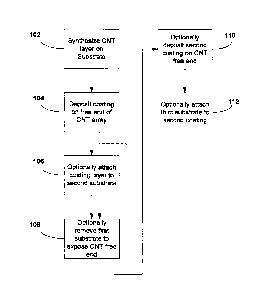
[0007] Figure 1 is a schematic of the process for the preparation of carbon
nanotube arrays
according to one embodiment of the present invention.
[0008] Figure 2 is a scanning electron micrograph of a carbon nanotube
array.
[0009] Figure 3 is a carbon nanotube device according to one embodiment of
the present
invention.
[0010] Figure 4 is a carbon nanotube device according to another embodiment
of the present
invention.
[0011] Figure 5 is a carbon nanotube device according to another embodiment
of the present
invention.
[0012] Figure 6 is a carbon nanotube device according to another embodiment
of the present
invention.
[0013] Figure 7 is a carbon nanotube device according to another embodiment
of the present
invention.
[0014] Figure 8 is a carbon nanotube device according to another embodiment
of the present
invention.
- 3b -
CA 02673705 2009-07-22
[0015] Figure 9 is a scanning electron micrograph of various coating layers
on a CNT array
according to one embodiment of the present invention.
[0016] Figure 10 is a scanning electron micrograph of a CNT device
according to the present
invention.
Detailed Description of the Invention
[0017] Although the following detailed description contains many specific
details for
purposes of illustration, one of ordinary skill in the art will appreciate
that many variations and
alterations to the following details are within the scope of the invention.
Accordingly, the
exemplary embodiments of the invention described below are set forth without
any loss of
generality to, and without imposing limitations thereon, the claimed
invention.
[0018] In one aspect, a method is provided for the preparation of a CNT array
that includes a
coating on at least one end of the array. The process for preparing arrays
according to one
embodiment of the present invention is shown in the schematic in Figure 1. In
a first step 102, a
substantially vertically aligned CNT layer is deposited on the surface of a
substrate. An
exemplary scanning electron micrograph of a CNT array is shown in Figure 2. In
a second step
104, a coating is applied to the exposed end of the CNT layer. The coating can
be metal,
diamond-like carbon (DLC), polymer, silicon carbide or the like and becomes
partially imbedded
or infused into the CNT layer. In an optional third step 106, the coating
layer is attached to a
second substrate. In an optional fourth step 108, following step 104 or 106,
the first substrate
can be removed to expose a free end of the CNT layer. In an optional fifth
step 110, a second
coating layer can be deposited on the newly exposed free end of the CNT layer
in a manner
similar to the deposition of the first layer. In an optional sixth step 112,
the second coating layer
-4-
CA 02673705 2009-07-22
can be attached to a third substrate. As provided the first and second coating
layers can be the
same, or they can be different. Similarly, the first, second and third
substrates can be the same or
they can be different.
[0019] In one embodiment, as shown in Figure 3, the CNT array can include a
substrate
material 10, a substantially vertically aligned CNT layer 12 and a coating 14
that partially infuses
into the CNT layer to provide a cap to the free end of the CNT layer distal
from the substrate
surface. The CNT layer 14 is attached to the substrate 12 at a first end, and
the coating 16 is
applied to a second end of the CNT layer.
[00201 The substrate 10 material can be a variety of known material
suitable for the growth of
CNTs. One exemplary substrate material is silicon dioxide (or a silicon
substrate that has been
oxidized), which provides the advantage of having a surface from which the CNT
layer may be
easily removed.
[0021] The carbon nanotubes 12 can be applied to the substrate 10 by known
means,
including but not limited to, chemical vapor deposition (CVD) synthesis or
plasma enhanced
chemical vapor deposition (PECVD), such as the Black Magic process (Slade
Gardner, et al.).
The chemical vapor deposition method is known in the art as being conducive to
growing CNT
arrays with the nanotubes that are substantially aligned and form a forest-
like growth that is
oriented substantially vertical to the surface of the substrate. In the
chemical vapor deposition
method, a carbon source gas is thermally decomposed at a predetermined
temperature in the
presence of a transition metal that acts as a catalyst, thereby forming a
carbon nanotube array. In
certain embodiments, the substrate may be prepared or conditioned by known
means prior to the
deposition of the CNTs to promote the growth and/or attachment on the surface
thereof. In
-5-
CA 02673705 2015-12-14
certain embodiments, the carbon nanotubes deposit in a manner such that the
nanotubes only
occupy about 10% of the total volume of the carbon nanotube forest. In certain
other
embodiments, the carbon nanotubes occupy between about 10% of the total volume
and about
20% of the total volume. In certain embodiments, with post processing
techniques, the CNTs
can occupy greater than about 50% of the total volume, greater than 75% of the
volume, and in
certain embodiments, greater than 90% of the total volume.
[0022] In certain embodiments, the CNT layer can be between about 1 micron and
several
centimeters in length. In certain other embodiments, the CNT layer can be
between about 1
micron and 100 microns. In certain embodiments, the CNT layer can be between
about 2
microns and 20 microns. It is understood that as the technology advances, CNT
arrays of lengths
longer than several centimeters will be possible.
[0023]
The coating or cap layer 14 can be a metal, ceramic, composite, alloy, or
polymer
material that partially infuses into the CNT layer. The coating or cap layer
14 can be applied to
the free ends of the CNT layer 12 by a variety of means. In certain
embodiments, the material
can be applied by vapor phase deposition, including, for example, chemical
vapor deposition
(CVD) PECVD, or physical vapor deposition. A variety of materials can be
applied to the
carbon nanotubes by these techniques, particularly metals, such as for
example, but not limited
to, titanium, aluminum, molybdenum, tungsten, tantalum, nickel, gold, silver,
copper, and the
like. In certain embodiments, alloys and compounds typically used in the
microelectronics
industry, including but not limited to, silicon dioxide, silicon-germanium,
silicon nitride, silicon
oxynitride and titanium nitride, can be applied by vapor phase deposition. In
certain
embodiments, diamond-like carbon or diamond-like nanocomposite coatings (such
as for
example, composites that include carbon, hydrogen, silicon and oxygen) can be
applied to the
-6-
CA 02673705 2009-07-22
ends of the carbon nanotubes by known methods. In certain other embodiments,
the metals can
be deposited on the surface by magnetron sputter deposition. The process
conditions for the
vapor phase deposition, such as temperature and power, can be varied to change
or modify the
resulting coating.
[0024] In certain embodiments, silicon carbide can be deposited on the surface
of the CNT
array by CVD techniques. Alternatively, a poly(methylsilyne) can be applied to
the CNT surface
as a solution and pyrolyzed to achieve the silicon carbide coating.
[0025] In certain embodiments, the coating can be applied to the exposed
carbon nanotube
end by depositing the material as a liquid. Materials suitable for liquid
deposition include, but
are not limited to, aluminum, solder (e.g., Pb-Sn), and silicon carbide
precursors, in addition to a
variety of organic and organometallic polymers. Penetration of the liquid can
be controlled by a
variety of means, including but not limited to, the amount of time the surface
is exposed to the
liquid, the viscosity of the liquid, the hydrophobicity of the liquid and the
conditions under
which the liquid is applied to the CNT layer (i.e., the layer is heated, the
liquid is heated, etc). In
certain embodiments wherein a polymer is used to infuse the carbon nanotube
array, the array
may undergo a cure of post deposition process, depending on the polymer used.
[0026] The coating infuses or imbeds itself into the carbon nanotube array. In
certain
embodiments, the coating infuses between about 1 and 3 microns into the carbon
nanotube array.
In other embodiments, the coating infuses between about 2 and 6 microns. In
yet other
embodiments, the coating can infuse the carbon nanotubes by up to about 10
microns. In yet
other embodiments, the coating can penetrate further into the array, up to and
including the entire
carbon nanotube array to the substrate.
-7-
CA 02673705 2009-07-22
[0027] The coating material can be selected based upon the desired properties
and end
application. In certain embodiments, the coating material, whether applied by
vapor phase or
liquid deposition, is selected such that the coefficient of thermal expansion
(CTE) closely
matches that of the substrate to which it is to be attached. Alternatively, in
another embodiment,
the coating material is selected such that the CTE of the coating material
closely matches that of
the CNT layer. In yet another embodiment, the coating material is selected to
achieve maximum
thermal conductivity. In yet another embodiment, the coating material is
selected for maximum
mechanical stability. In yet another embodiment, the coating material is
selected to achieve
maximum electrical conductivity. In yet another embodiment, the coating
material is selected
for its optical behavior. In yet another embodiment, the coating material is
selected to maximize
adhesion to the substrate to which is will be attached. In yet another
embodiment, the coating
material can include more than one material. In embodiments wherein the CNT
array is
positioned between two coating layers, the coatings can be the same, or in
alternate
embodiments, the coatings can be different. In yet other embodiments, a
coating may include
more than one material.
[0028] In another embodiment, the coating layer on the CNT array can provide
additional
means from which to manipulate the CNT array. The metal layer provides
mechanical strength
and electrical conductivity to the system. In certain embodiments, the metal
layer can be
attached to a second substrate material, as shown for example, in Figure 4,
wherein the metal
coating 14 is attached or adhered to a second substrate 16. Exemplary
materials to adhere the
metal coating 14 to a second substrate 16 include known adhesives (including
but not limited to
pressure adhesives and tapes), epoxies and other heat or chemically activated
adhesives and
-8-
CA 02673705 2009-07-22
solders, as is known in the art. Preferably, the means for attaching the
second substrate are
selected based upon the end use of the array.
[0029] In certain embodiments, as shown in Figures 5 and 7, the initial
substrate 10 can be
removed from the array to expose the first end 17 of the CNT layer 12, thereby
allowing the
CNT layer to be manipulated. The coated CNT layered structure can typically be
easily removed
from the substrate on which the CNTs are initially grown. Generally, the
adhesion of the CNT
layer to the substrate is poor, thereby facilitating removal. In certain
embodiments, only a small
amount of effort may be all that is required to peel off the coated CNT layer
from the substrate.
As noted previously, in certain embodiments, the CNT array can be prepared on
a silicon
substrate, which thereby facilitates the removal of the carbon nanotubes from
the substrate
surface. In certain embodiments, heat may be applied to the CNT array to
facilitate the removal
of the array from the substrate. In certain embodiments, the CNT array may be
heated to about
500 C in air to promote removal of the CNT and coating layer from the growth
substrate. In
certain other embodiments, a chemical release agent can be applied to the CNT
and coating layer
to facilitate removal of the carbon nanotube array from the substrate.
[0030] As shown in Figure 6, a second coating layer 18 can be applied to the
newly exposed
CNT layer 17 according to the deposition means previously described. The
second coating 18
can be the same material as was applied as the first coating 14, or it can be
a different material.
The resulting structure can have a sandwich-like structure (e.g. metal-CNT
layer-metal or metal-
CNT layer -ceramic).
-9-
CA 02673705 2009-07-22
[0031] As shown in Figure 8, the second coating 18 can be attached or adhered
to a third
substrate 20 by the means previously described with respect to the attachment
of second
substrate 16 to the first coating layer 14.
[0032] Figure 9 shows a scanning electron micrograph from a scanning electron
microscope
(SEM) of an exemplary CNT array wherein a vertically aligned CNT array is
positioned between
titanium coatings. Figure 10 shows scanning electron micrographs for the
deposition of
aluminum, copper and diamond-like carbon (DLC) onto one surface of a CNT
array.
[0033] In certain embodiments, one or both of the surfaces of the CNT layer
can be modified
by chemical or physical means prior to the deposition of the coating layer. In
certain
embodiments, the surface of the CNT layer can be exposed to a plasma source
prior to deposition
of the coating layer.
[0034] Characterization of the coated structure demonstrates that the CNTs of
the coated CNT
arrays are not affected by the coating process as Raman spectroscopy reveals
that the materials
are the same, before and after the application of the coating layer.
[0035]
In certain embodiments, the tensile strength of the metal-CNT layer interface
is at least
about 5 MPa. In certain other embodiments, the tensile strength is at least
about 7 MPa. In yet
other embodiments, the tensile strength is at least about 8 MPa. In yet other
embodiments, the
tensile strength is greater than at least about 10 MPa.
[0036] Individual single carbon nanotubes have high tensile strength and high
thermal
conductivity along their axis. The typical CNT array is characterized in that
it is compressible
such that it is both structurally and mechanically similar to an open-celled
foam structure. The
-10-
CA 02673705 2009-07-22
typical CNT arrays prepared according to the methods provided herein have a
conductivity of at
least about 10 W/mK, preferably at least about 15 W/mK.
[0037] In certain embodiments, a thick coating can be applied to the CNT array
to provide a
system that is self supporting. In certain embodiments wherein coating is a
metal layer about 5
microns thick. In certain other embodiments, the metal coating layer can be
about 4 microns
thick. In yet other embodiments, the metal layer is between about 4 and 7
microns thick. As is
understood in the art, the thickness of the coating layer required for the
array to be self
supporting varies based upon the particular coating material and the
parameters under which it is
deposited.
[0038] Infusion of the coating into the top region or top few microns of the
carbon nanotube
array can lead to improved adhesion and higher conductivity of the coating to
the carbon
nanotube array as compared with a coating that is not infused into the CNT
array. By limiting
the infusion of the coating to the top region or top few microns of the CNT
array, the bulk
properties of the carbon nanotube array, such as for example, compliancy, can
be preserved. The
amount of infusion can be controlled through choice of such parameters as
coating material,
method of deposition, and deposition parameters.
[0039] Controlling the coating thickness and the amount of infusion of the
coating into the
CNT array are aspects of the invention which allows for the manipulation of
the coated CNT
arrays, and may have additional applications outside of the primary focus of
this disclosure. For
example, the CNT array has been characterized elsewhere to have excellent
optical absorbance
(e.g. it is very black). The coated CNT array can be applied to an object such
that the foil side is
-11-
CA 02673705 2009-07-22
applied or adhered to the surface of the object, such that the uncoated side
of the CNT array were
exposed, thereby providing an alternative to painting an object black.
[0040] The CNT array can also be used as a thermal interconnect, wherein a
first object can
be attached to the coated face of the CNT array (e.g. by soldering or with
epoxy or any other
known adhesive) and the second object can be attached or adhered to the
opposite face of the
CNT array (Figure F). In this device, there is no mechanical connection
between the CNT array
and the surface of the second object, however the thermal conductivity though
the CNT array
would still be high. Thermal conduction may be decreased if the system
experiences mechanical
stress.
[0041] Exemplary devices that can be prepared from the carbon nanotube devices
described
herein include devices suitable for the removal of heat from an electronic
device. The carbon
nanotube array can be connected to a cold plate or thermal spreader at one
end, thereby
facilitating the transfer of heat through the carbon nanotube array.
[0042] Although the present invention has been described in detail, it should
be understood
that various changes, substitutions, and alterations can be made hereupon
without departing from
the principle and scope of the invention. Accordingly, the scope of the
present invention should
be determined by the following claims and their appropriate legal equivalents.
[0043]
The singular forms "a", "an" and "the" include plural referents, unless the
context
clearly dictates otherwise.
-12-
CA 02673705 2015-12-14
. .
[0044] Optional or optionally means that the subsequently described
event or circumstances
may or may not occur. The description includes instances where the event or
circumstance
occurs and instances where it does not occur.
[0045] Ranges may be expressed herein as from about one particular value,
and/or to about
another particular value. When such a range is expressed, it is to be
understood that another
embodiment is from the one particular value and/or to the other particular
value, along with all
combinations within said range.
-13-