Note : Les descriptions sont présentées dans la langue officielle dans laquelle elles ont été soumises.
CA 02673963 2009-06-25
WO 2008/082302 PCT/NL2008/050002
P79330PC00
Title: Electrical measuring device, method and computer program product
The invention relates to an electrical measuring device for performing
an electrical impedance measurement, comprising a measuring unit which
is provided with the impedance to be measured and a passive resonance
circuit connected thereto for generating a measuring signal to be received by
a separate active transmitting and receiving unit for determination of the
electrical impedance upon reception of an interrogation signal transmitted
by the active transmitting and receiving unit.
United States patent publication US 6 870 376 describes an electrical
measuring device for performing an electrical impedance measurement for
the purpose of determining the humidity level in, for instance, the soil or
the
substrate in which a plant is rooted. The impedance is basically a capacitor
that varies depending on the humidity near the capacitor. Thus, in an
electrical manner, the humidity level can be locally determined.
Further known, for instance from the scientific article "Remote Query
Resonant-Circuit Sensors for Monitoring of Bacteria Growth: Application to
Food Quality Control" by Keat Ghee Ong and others, published in Sensors,
pp. 219-232, 2002, is an electrical measuring device according to the opening
paragraph hereof, where an impedance designed as a capacitor is part of a
passive resonance circuit of a measuring unit which is galvanically
decoupled from an element of a separate transmitting and receiving unit
that transmits and receives electromagnetic fields. By electromagnetically
coupling the transmitting and receiving unit to the resonance circuit,
information about the capacitor can be gained, since capacitive values of the
capacitor - which in their turn are dependent upon for instance a local
humidity level - affect the behavior of the resonance circuit. The measuring
device can be employed for checking for instance bacterial growth in foods.
CA 02673963 2009-06-25
WO 2008/082302 PCT/NL2008/050002
2
During operation of the measuring device, the transmitting and
receiving unit transmits an electromagnetic interrogation signal, whereupon
the passive resonance circuit generates a reflective measuring signal which
is thereupon received and analyzed by the separate transmitting and
receiving unit. Depending on actual values of the capacitor, the peak
frequency of the measuring signal can vary, so that a measure is obtained
for the humidity adjacent the capacitor in the measuring unit.
Advantages of such a contactless impedance measurement are inter
alia low manufacturing costs per measuring unit and a relatively long life
because of the use of passive components, and ease of use in performing the
measurement, since the user hardly if at all needs to perform any
mechanical operations which are time consuming and tend to lead to
measuring errors, such as placing a measuring unit in a sample and
removing the measuring unit from the sample.
For obtaining a qualitatively good contactless impedance
measurement, the measuring unit is calibrated using a reference
measurement, where the impedance is situated in a conditioned space. Such
a reference measurement is performed prior to in situ placement of the
measuring unit.
This involves the problem that upon placement of the measuring unit,
practically no reference measurement is possible anymore, while yet
parameters of the resonance circuit may drift, for instance through ageing.
This renders the impedance measurement less pure. In addition, carrying
out the reference measurement is experienced as user unfriendly and labor
intensive.
The object of the invention is to provide an electrical measuring
device according to the opening paragraph hereof, whereby, whilst
maintaining the advantages, the disadvantages mentioned are obviated. In
particular, the object of the invention is to provide an electrical measuring
device according to the opening paragraph hereof whereby the accuracy of
CA 02673963 2009-06-25
WO 2008/082302 PCT/NL2008/050002
3
the impedance measurement is augmented. To that end, the measuring unit
is furthermore arranged for, depending upon the interrogation signal,
generating with the aid of the resonance circuit a reference signal to be
received by the active transmitting and receiving unit.
By providing a measuring device whereby during a reference
measurement, depending upon the interrogation signal, with the aid of the
resonance circuit a reference signal to be received by the active transmitting
and receiving unit is generated, the reference measurement can
advantageously take place at any location and time, also there where the
impedance measurement is to be carried out. On the basis of the reference
measurement, which can thus be carried out according to need and as often
as desired, the impedance can be calibrated, so that the accuracy of the
impedance measurement augments.
Moreover, correction for drifting parameters of the resonance circuit
is enabled. In addition, the reference measurement where the measuring
unit is placed in a conditioned space, has become redundant, which
enhances ease of use and reduces extra costs in placing the measuring unit
to a large extent. Also, manufacturing tolerances in respect of elements in
the resonance circuit may be less stringent, which contributes to a further
cost price decrease.
When a single transmitting and receiving unit is used in combination
with a plurality of measuring units, this entails a cost advantage since the
measuring unit can consist of relatively few, inexpensive components, while
relatively complex electronics for analyzing the measuring and reference
signals can be implemented in the transmitting and receiving unit.
In addition, elegantly, components are saved on by transmitting both
the measuring signal and the reference signal with the aid of the resonance
circuit.
It is noted that the term impedance may be understood to cover a
variety of types of passive discrete electrical elements, as a capacitor,
CA 02673963 2009-06-25
WO 2008/082302 PCT/NL2008/050002
4
inductor and/or resistor, as well as materials displaying a capacitive,
inductive and/or resistive behavior. In this connection, also terms such as
dielectric behavior or the conductivity of a material are customary. The
technique of measuring an electrical impedance as a measure for a physical
change is sometimes designated as impedance spectroscopy.
The reference signal is generated depending upon the interrogation
signal. The nature of this dependency may be implemented in various ways.
Thus, for instance, the frequency and/or amplitude of the interrogation
signal may vary to cause, as desired, a measuring aignal or a reference
signal to be generated. Also, the interrogation signal may be provided with a
code for generating a measuring signal or a reference signal. For that
matter, it may also be elected to design the interrogation signal such that
both the measuring signal and the reference signal are generated.
Preferably, the signals transmitted by the measuring unit are
narrow-band. The measuring signal and the single or multiple reference
signals are then situated in a limited bandwidth, so that in practice the
electrical measuring device can be used in an available frequency band.
Thus, the frequencies of the measuring signal and of the single or multiple
reference signals may for instance differ from each other by a few percents
or less.
Advantageously, the measuring unit may be arranged for, depending
upon the interrogation signal, generating with the aid of the resonance
circuit a specific reference signal from a plurality of reference signals. By
enabling transmission of a plurality of reference signals, more information
of the measuring system can become available at the separate transmitting
and receiving unit, for instance for improving the measurement or for
obtaining other information about the measuring unit, such as identification
information of the measuring unit.
According to an aspect of the invention, the measuring unit and the
separate active transmitting and receiving unit are arranged for wireless
CA 02673963 2009-06-25
WO 2008/082302 PCT/NL2008/050002
mutual signal transfer, thus allowing a contactless measurement. As a
result, the ease of use of the electrical measuring device increases, since no
wire connections are needed then for establishing signal transfer between
the separate active transmitting and receiving unit and the measuring unit.
5 Alternatively, however, signal transfer can also be effected with the aid of
a
wire connection, for instance to realize a saving of costs or to improve the
reliability and/or sensitivity of the signal transfer.
According to an aspect of the invention, the measuring unit can
furthermore comprise a reference circuit for, depending upon the
interrogation signal, generating with the aid of the resonance circuit a
reference signal. By influencing the amplitude characteristic in a controlled
manner in this way, an absolute calibration can be carried out with the
extra measurement.
According to another aspect of the invention, the electrical properties
of the resonance circuit remain invariant, while the measuring unit is
furthermore arranged for, depending upon the interrogation signal,
generating with the aid of the resonance circuit a reference signal having a
central frequency that differs from the central frequency of the measuring
signal. In this way, extra information about the characteristic becomes
available, so that likewise an absolute calibration can be carried out.
By connecting the additional reference circuit to the resonance circuit,
the circuit can be employed for generating both the measuring signal and
the reference signal, so that the number of electrical components of the
measuring unit may be saved on. Alternatively, however, the additional
reference circuit may also be part of a separate resonance circuit, so that
measuring signal and reference signal are generated separately.
By connecting the impedance to be measured or the additional
reference circuit to the resonance circuit via a switching element, a
measuring or reference signal may be generated depending upon the state of
CA 02673963 2009-06-25
WO 2008/082302 PCT/NL2008/050002
6
the switching element. The state of the switching element can be influenced
by the interrogation signal for obtaining the desired signal.
The additional reference circuit may be placed in a space which is at
least partially conditioned, preferably in such a manner that the electrical
properties of the reference circuit are substantially invariant compared with
corresponding property variations of the impedance to be measured, so as to
obtain a meaningful reference measurement.
By making the additional reference circuit of passive design, the
circuit of the measuring unit can be manufactured particularly cheaply,
while the operational life is practically unlimited. However, the additional
reference circuit may also be designed with a compact energy source, so that
a simplification in the complexity of the signal to be analyzed may be
achieved.
Furthermore, the invention relates to a method.
Also, the invention relates to a computer program product.
Further advantageous embodiments of the invention are represented
in the subclaims.
The invention will be further elucidated on the basis of exemplary
embodiments which are represented in the drawing. In the drawing:
Fig. 1 shows a circuit of a first embodiment of an electrical
measuring device according to the invention;
Fig. 2 shows a circuit of a second embodiment of an electrical
measuring device according to the invention;
Fig. 3 shows a circuit of a third embodiment of an electrical
measuring device according to the invention;
Fig. 4 shows a time domain diagram of signals that occur in the
circuit of Fig. 3;
Fig. 5 shows an amplitude spectrum of the signals of Fig. 3;
Fig. 6 shows a circuit of a fourth embodiment of an electrical
measuring device according to the invention;
CA 02673963 2009-06-25
WO 2008/082302 PCT/NL2008/050002
7
Fig. 7 shows an amplitude spectrum of a current through a coil;
Fig. 8 shows a circuit of a fiffth embodiment of an electrical measuring
device according to the invention;
Fig. 8A shows a square wave signal;
Fig. 8B shows a fundamental harmonic and two second-order
harmonics;
Fig. 9 shows a circuit of a sixth embodiment of an electrical
measuring device according to the invention;
Fig. 10 shows a first amplitude spectrum of a signal generated by the
measuring device;
Fig. 11 shows a second amplitude spectrum of a signal generated by
the measuring device;
Fig. 12 shows a first schematic block diagram of a measuring unit;
and
Fig. 13 shows a second schematic block diagram of a measuring unit.
The figures are only schematic representations of preferred
embodiments of the invention. In the figures, equal or corresponding parts
are designated by the same reference characters.
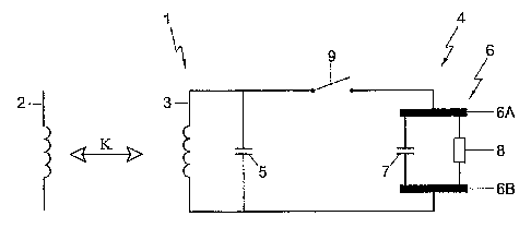
Fig. 1 shows a circuit 1 of a first embodiment of an electrical
measuring device according to the invention.
The circuit 1 is arranged for performing a contactless impedance
measurement. The circuit comprises two coils 2, 3 which are galvanically
separated and during operation of the measuring device effect an
electromagnetic coupling K. A first coil 2 is arranged in a separate active
transmitting and receiving unit, the second coi13 is part of a passive
resonance circuit 4 in a measuring unit. Through the electromagnetic
coupling, a mechanically speaking contactiess measurement can be
performed. It is noted that the electromagnetic coupling or radio connection
may also be effected otherwise, for instance using electrical and/or magnetic
dipoles.
CA 02673963 2009-06-25
WO 2008/082302 PCT/NL2008/050002
8
As is apparent from Fig. 1, the resonance circuit 4 is passive, so that
the measuring unit can be advantageously designed without batteries.
Connected in parallel to the coil 3 of the resonance circuit 4 are a
reference capacitor 5 and an impedance 6 to be measured. The reference
capacitor 5 is a possible implementation of an additional passive reference
circuit. The impedance 6 to be measured between two impedance electrodes
6A, 6B is connectible via a switch 9 and has been modeled as a measuring
capacitor 7 and measuring resistor 8 mutually connected in parallel, which,
for instance, may typically have a value of about 100 pF and about 1,000 0,
respectively. The values can depend on the material to be measured, the
surface of and the distance between the electrodes, as well as on the
resonance frequency.
The operation of the measuring device is as follows. The coil 2 of the
transmitting and receiving unit transmits an electromagnetic interrogation
signal, for instance a radio wave having a frequency of 1 MHz, which is
captured by the coil 3 of the resonance circuit 4, which is so tuned that a
measuring signal or reference signal is generated, depending on the state of
the switch 9. The measuring signal or reference signal is thereupon
captured by the coil 2 of the transmitting and receiving unit, for analysis.
By determining characteristics of the measuring signal or reference signal,
such as spectral and/or amplitude information, information about electrical
properties of the resonance circuit 4 can be determined. The impedance
electrodes 6A, 6B can be placed in material to be examined, so that
dielectric variations of the material between the impedance electrodes 6A,
6B can be determined. The other components of the resonance circuit 4 are
accommodated in a casing, also referred to as package, for the purpose of
durable use.
When the switch 9 is open, the resonance circuit is only formed by the
coil 3 and the reference capacitor 5, so that a reference signal is obtained.
In
the closed state of the switch 9, the characteristics of the resonance circuit
4
CA 02673963 2009-06-25
WO 2008/082302 PCT/NL2008/050002
9
are also formed by the impedance 6, so that a measuring signal is obtained.
Thus, by the influence of the measuring capacitor 7 the peak frequency can
be detuned and by the influence of the measuring resistor 8 the maximum
spectral amplitude can diminish and/or spectral smearing can occur.
By operating the switching element 9 depending upon the
interrogation signal and varying the frequency of the interrogation signal,
for instance with a frequency shift, also referred to as frequency sweep, a
detuned peak frequency can be detected.
The electrical measuring device according to the invention can be
advantageously used for contactless measurement of local material
characteristics, since the condition of material influences the electrical
behavior of the impedance to be measured and hence the measuring signal
that is generated by the resonance circuit. Changes in material relate for
instance to moisture content, acidity and/or mineral concentration. Also, the
electrical permittivity of for instance ceramics may be a measure for
external moisture tension. Furthermore, a plastic layer provided on a
substrate may be sensitive to ambient influences such as temperature,
concentrations of gases or a pH value. Thus, the measuring device can for
instance be implemented as a water content sensor for soil and/or substrate
in which flowers, plants and/or other crops are rooted. The measuring device
is then usuable for monitoring purposes, for instance in potted plants of
growers or in agricultural lots. Optionally, the measuring device may be
coupled to irrigation systems.
In additions, also other fields of application are conceivable, for
instance in the field of bio-nanotechnology for observing changes in a
biological substrate. Concrete examples of this are sensors for the food
industry, such as sensor for checking milk quality, ageing of fruit juices
and/or bacterial growth in meat products. Naturally, more applications are
conceivable, for instance for determining the water content of a porous
CA 02673963 2009-06-25
WO 2008/082302 PCT/NL2008/050002
material, such as sand or cement, medical applications, water management
and uses in the oil industry.
Thus, in practice, the measuring unit can be placed in the
environment to be measured. The separate transmitting and receiving unit
5 can be included in a mobile, optionally portable module and be carried along
by a user. Thus, one and the same transmitting and receiving unit can be
coupled contactlessly to a plurality of measuring units for the purpose of
performing a contactless measurement. Consequently, savings on
components in the measuring unit can be utilized still further.
10 Preferably, the parameters of the coil 3 and the reference capacitance
5 of the measuring unit are chosen such that a high quality factor is
obtained. Furthermore, preferably, parameters of the components of the
additional reference circuit are chosen such that a main frequency of the
measuring signal and a main frequency of the reference signal differ
mutually by about a few percents, so that requirements regarding
bandwidth for equipment in the transmitting and receiving unit remain
limited and secondary effects do not contribute significantly. In principle,
however, parameters may also be chosen such that the main frequencies
mentioned are further apart from each other. For the circuit as shown in
Fig. 1, there is a quadratic relation between the ratio of the main
frequencies on the one hand and the ratio of the capacitors on the other.
The switching element 9 in Fig. 1 is designed as a mechanical switch
which can be operated via an external field. Thus, a reed relay, for instance,
switches as a result of an external magnetic field. To that end, the separate
transmitting and receiving unit may for instance be equipped with an
actuator for generating the external magnetic field.
Preferably, an automatic amplitude control is used by the
transmitting and receiving unit, so that the power loss resulting from the
distance and matter between the transmitting and receiving unit and the
measuring unit is corrected for.
CA 02673963 2009-06-25
WO 2008/082302 PCT/NL2008/050002
11
Fig. 2 shows a circuit of a second embodiment of an electrical
measuring device according to the invention, in which the switching element
9 is designed as a semiconductor switch, in particular a MOSFET 9A which
is implemented via a rectifying circuit with a diode 10 and a capacitor 11.
Upon an interrogation signal of a relatively low amplitude, the MOSFET 9A
remains closed, so that a reference signal is generated. However, if an
interrogation signal of a relatively high amplitude is received, the MOSFET
9A enters the conductive state, so that a measuring signal is generated.
Naturally, also other semiconductor switches are possible. In addition, the
circuit may be so arranged that upon an interrogation signal of a relatively
low amplitude a measuring signal is generated, while upon an interrogation
signal of a relatively high amplitude a reference signal is generated.
Furthermore, the switching element 9 may be designed as an
electrical non-linear component, for instance a diode 9B, as shown in Fig. 3.
As is the case with the above-described MOSFET 9A, the diode 9B enters
the conductive state when the interrogation signal has an amplitude that is
relatively high. During the switching on and off of a stationary interrogation
signal, there occurs a switch-on and switch-off phenomenon, respectively, in
which both the measuring signal and the reference signal are integrated.
For a proper operation of the resonance circuit, the diode 9B
preferably has a low diode voltage, a high reverse voltage and a low junction
capacitance.
Figs. 4 and 5 show respectively a time domain and a spectral diagram
of signals generated by the resonance circuit 4 in the circuit as shown in
Fig. 3. The voltage V is plotted against time t and frequency f, respectively.
The signals have a reference component 12 at the resonance frequency
1 MHz and a measuring component 13 around a shifted frequency near
about 0.85 MHz. The measuring component 13 has a certain spectral width
caused by measuring resistance 8.
CA 02673963 2009-06-25
WO 2008/082302 PCT/NL2008/050002
12
Fig. 6 shows a circuit of a fourth embodiment of an electrical
measuring device according to the invention. Here, the switching element 9
is designed as a circuit of two diodes 9B, 9C which are respectively
connected to the impedance 6 to be measured and an additional passive
reference circuit. Connected parallel to the coil 3 of the measuring unit is a
resonance capacitor 16 for obtaining a resonance circuit 4. The additional
passive reference circuit, also called reference impedance, comprises a
reference capacitor 14 and a reference resistor 15 mutually connected in
paraIIel. Naturally, the additional passive reference circuit may also be
designed differently, for instance as only the capacitor 14 or the resistorl5
or in combination with an additional coil.
Through the structure of the circuit, the positive part of a harmonic
interrogation signal is presented to the impedance 6 to be measured, while
the negative part is presented to the reference impedance 14, 15. Moreover,
higher harmonics of the interrogation signal arise. The amplitude and phase
of the higher harmonics contain information about the impedance 6 to be
measured and the reference impedance 14, 15. In the specific case where the
measuring and reference impedance 7, 8; 14, 15 are equal, the even
harmonics quench. Also in other situations of the reference and measuring
impedance 14, 15; 6, the parameters of the measuring impedance 6 can be
determined on the basis of the information about the harmonics. Here, use
can be made of both amplitude and phase information of various spectral
components.
Fig. 7 shows an amplitude spectrum of the electrical current through
the second coil 3, which is explained as follows. The sine-shaped current
through each diode branch separately causes even harmonics because of the
non-linearity of the diode. Because one diode is conductive during the
positive part of the sine and the other during the negative part, the even
harmonics in the two diode branches, as illustrated in Fig. 8, cancel out,
while electrical quantities such as a square wave 60, a fundamental
CA 02673963 2009-06-25
WO 2008/082302 PCT/NL2008/050002
13
harmonic 61 and two second-order harmonics 62, 63 are shown with respect
to respective terminals 18, 18, 51, 52 of the second coil 3 and the diodes 9B,
9C in Figs. 8A and 8B. When the impedances 6, 19 in the diode branches are
equal to each other, the current through the second coil 3 is therefore built
up only from odd harmonics of an original square wave 60 induced by the
first coil 2. When the impedances 6, 19 differ, the even harmonics in the two
diode branches are not equal anymore leaving a differential current in the
second coil 3. Consequently, the current through the second coil 3 comprises
both even and odd harmonics. The amplitude spectrum may then for
instance look as shown in Fig. 7, where the amplitude A of the harmonics
al,..., alO is shown as a function of a normalized frequency f. Generally, the
amplitude of the even harmonics is a function of the inequalities of the
impedances 6, 17 and the amplitude of the original square wave 60. For that
reason, from the amplitude of the received signal, the inequality in the two
impedances can be derived. The amplitude of the odd harmonics is virtually
exclusively a function of the square wave 60.
Phase information can for instance be obtained by generating higher
harmonics locally at the transmitting and receiving unit and applying
synchronous detection to determine the phase relation with the spectrum
components of the signal generated by the resonance circuit. A synchronous
detector has the advantage of a very high dynamic range and a low
interference sensitivity.
To realize a constant operation point for the diodes, the amplitude of
the first harmonic may be so controlled that the amplitude of one of the
transmitted odd harmonics remains in a fixed ratio to the amplitude of the
first harmonic, regardless of the distance between the two coils 2, 3. The
amplitude ratio between the even and odd harmonics is then uniformly fixed
and is an absolute measure for the inequality between the impedances.
The inequality in the two branches can also be realized by applying
an extra voltage or current across or through the two impedances, for
CA 02673963 2009-06-25
WO 2008/082302 PCT/NL2008/050002
14
instance by using diodes with different base emitter voltages. Thus, the
even harmonic can be modulated with another signal which contains for
instance an identification code.
Fig. 9 shows a circuit of a sixth embodiment of an electrical
measuring device according to the invention, where the circuit from Fig. 3
has been expanded to include an extra subcircuit which is connected parallel
to the second coil 3. The extra subcircuit is a series connection of two
diodes
9D, 9E and an extra impedance 20. By raising the amplitude of the
interrogation signal still further, also the extra subcircuit can be rendered
conductive, so that in response to the interrogation signal yet another signal
is transmitted, differing from the measuring signal and reference signal,
since also the extra impedance 20 has in fact been additionally connected.
As a consequence, an extra measurement can be performed, for instance of
the temperature. Thus, setting of the amplitude level of the interrogation
signal allows selecting between different types of response signals, thus
allowing a coded interrogation of the measuring unit. More generally, the
measuring unit is provided with an extra circuit for, depending upon the
interrogation signal, generating an extra signal to be wirelessly received by
the active transmitting and receiving unit.
If desired, the pattern of the extra subcircuits may be further
continued with a parallel circuit in which three or more diodes are series-
connected. Furthermore, such an extra subcircuit may also be used in
combination with other embodiments of the invention, for instance as shown
in Figs. 2 and 6.
The transmitting and receiving unit is preferably provided with a
processor for processing the measuring and reference signal to determine
the electrical impedance.
The method for carrying out such processing operations can be
practiced both with the aid of specific processor components and with the
aid of specific program.
CA 02673963 2009-06-25
WO 2008/082302 PCT/NL2008/050002
Optionally, calculations of the reference signal may performed on one
or more defined harmonics and calculations of the measuring signal on the
basis of one or more other harmonics.
According to an aspect of the invention, signals are processed by the
5 separate transmitting and receiving unit for determination of the electrical
impedance. This can be executed in different ways.
In a first embodiment, during a single or multiple reference
measurement an impedance connected to the resonance circuit can vary by
switching one or more reference circuits on or off using one or more
10 switches. As a result, obviously, the amplitude characteristic of the
resonance circuit changes. This characteristic changing per measurement is
measured at a fixed frequency. In principle, however, it is also possible to
choose any random other frequency in consecutive measurements. In
addition, a peak frequency of the amplitude characteristic changing per
15 measurement may be determined. In this first embodiment, the amplitude
characteristic can, as it were, shift as a function of the frequency.
In a practical embodiment according to the invention, in case of a
plurality of received signals at a fixed, predetermined frequency a
normalized amplitude of the integral resonance circuit impedance can be
determined. Fig. 10 shows a first amplitude spectrum A with three
amplitude characteristics cl, c2, c3 as a function of the frequency f, that
correspond with a measuring signal and two reference signals which have
been generated by the measuring unit. At a fixed frequency fc, the
corresponding normalized amplitudes Al, A2, A3 of the integral resonance
circuit impedance are determined. The frequency-dependent integral
resonance circuit impedance can be modeled on the basis of three
parameters, viz. a resistivity or conductivity, a capacitance and an
inductivity. Furthermore, a normalization is done through multiplication of
the resonance circuit impedance by a scalar transfer function of the transfer
between the measuring unit and the separate transmitting and receiving
CA 02673963 2009-06-25
WO 2008/082302 PCT/NL2008/050002
16
unit. On the assumption that the scalar transfer function is invariant
during the various measuring signals and that the other three parameters
that characterize the resonance circuit impedance are also constant or vary
in a controlled manner through operation of switches, a set of equations may
be drawn up from which the three parameters and the scalar transfer
function may be resolved. From this, the impedance to be measured can
then be determined. On the assumption that the inductivity is sufficiently
known, three measurements are then sufficient to determine the three other
parameters, viz. the scalar transfer function, the conductivity and the
capacity.
In this context, it is noted that the accuracy of the measurement as a
whole can be improved by predetermining the inductivity more accurately,
for instance by calibration or trimming of the inductivity. Furthermore,
other parameters, such as the conductivity and/or the capacity may be
determined better, for instance by a measurement in the air. Furthermore, a
reference capacity may be additionally included in the circuit to obtain a
better estimate of the inductivity through a reference measurement.
It is noted that instead of three measurements, also a different
number of measurements may be performed for determining the impedance,
for instance two measurements where through extrapolation an estimate of
the third unknown parameter can be obtained, or more than three
measurements, for instance four measurements, so that the accuracy of the
measurement can be improved, for instance using a least square method.
In a second embodiment for processing signals, the measuring unit is
arranged, depending upon the interrogation signal, to generate with the aid
of the resonance circuit a reference signal having a central frequency that
differs from the central frequency of the measuring signal. Thus, the value
of the electrical impedance to be measured can be determined by
determining the amplitude characteristic of the normalized resonance
impedance at different frequencies. Fig. 11 shows a second amplitude
0
CA 02673963 2009-06-25
WO 2008/082302 PCT/NL2008/050002
17
spectrum A with a single amplitude characteristic cl as a function of the
frequency f which corresponds to a measuring signal and two reference
signals generated by the measuring unit. By determining the amplitudes
A2, A2, A3 at different frequencies fcl, fc2, fc3, the value of the electrical
impedance can be derived on the basis of the above-mentoned modeling. By
choosing the different frequencies at which the amplitude spectrum is
measured at a relatively steep slope of the amplitude spectrum, the
resolution of the measurement can be increased.
According to another aspect of the invention, the interrogation signal
can be transmitted at a first frequency, for instance about 27 MHz, while
the measuring signal andlor the reference signal is determined at a
different, second frequency. To this end, the measuring unit may be
arranged to transmit the measuring signal at the second frequency, for
instance about 13.5 MHz. It is also possible for the measuring unit to
transmit a measuring signal whose energy is substantially concentrated
around the first frequency, while the receving unit measures the measuring
signal at the second frequency. By using different frequencies for the
transmitted signal and return signal, interference, for instance due to
inductance of the transmitter unit, be can controlled. Also, the effect of
higher harmonics can be controlled.
Fig. 12 shows a diagrammatic block diagram of a measuring unit
according to the above-outlined principle. The measuring unit 70 comprises
a receiver 71 which passes a received signal on to a receiver circuit 72,
connected thereto, which is tuned to a first frequency, in this case for
instance about 27 MHz. Further, the unit 70 comprises a frequency divider
73 which is supplied by a supply unit 75 which is provided with energy by
the receiver circuit. Furthermore, the frequency divider 73 is connected to a
multiple frequency divider 74 and to a resonance circuit 77 which in turn is
connected to measuring electrodes 76. The multiple frequency divider 74
functions to successively link up a first and a second reference circuit 79,
80,
CA 02673963 2009-06-25
WO 2008/082302 PCT/NL2008/050002
18
each comprising a known reference capacity. As a result, in each case a
sequence of the measuring signal and two reference signals is transmitted
by the measuring unit 70. The measuring signal and the two reference
signals are all directed via the resonance circuit 77 to a transmitter 78
connected thereto, in order to be transmitted, so that the separate
transmitting and receiving unit can received and process these signals. The
resonance circuit 77 is tuned to 13.5 MHz. In this embodiment of the
measuring unit, the frequency of the signals hence remains constant while
the impedance connected to the resonance circuit alters.
According to another aspect of the invention, the interrogation signal
comprises a modulated signal, for instance a primary signal at for instance
about 27 MHz which, through amplitude modulation, has been modulated
on a carrier of for instance 2.4 GHz. The modulated signal can be
demodulated on the measuring unit, for instance with a diode circuit, so
that the measuring unit in response thereto can transmit a measuring
signal and/or a reference signal.
Fig. 13 shows a schematic block diagram of a measuring unit
according to the above-outlined principle. The measuring unit 70 comprises
a receiver 71 which passes a received signal on to a receiver circuit 81,
connected thereto, which is tuned to a first frequency, in this case for
instance about 2.4 GHz. The thus filtered signal is passed on to an
amplitude modulation detector, for instance designed as a diode, for
extracting the baseband signal, for instance a signal of approximately 27
MHz. This signal, depending upon the measuring impedance that is
connected to the measuring electrodes, is transmitted via a transmitter 78
for reception by the separate transmitting and receiving unit. Instead of a
signal of 27 MHz, naturally also a slightly altered signal may be used, for
instance 26.9 MHz or 27.1 MHz. By successively using signals with slightly
altered frequencies, thus a scheme may be used whereby the characteristics
of the impedance connected to the resonance remain unchanged, while extra
CA 02673963 2009-06-25
WO 2008/082302 PCT/NL2008/050002
19
information is gained by determining the amplitude spectrum at different
frequencies.
It is noted that the electrical measuring device comprises only a
single resonance circuit, so that only a relatively small number of
components are required. Moreover, the measuring unit is relatively
compact. In addition, a narrow-band measurement is carried out, so that in
practice the measurement can be carried out reliably within a small
bandwidth. The invention is not limited to the exemplary embodiment
described here. Many variations are possible.
Thus, the additional passive reference circuit may be implemented
differently, for instance to additionally comprise a reference resistance or
to
comprise only a reference resistance.
Furthermore, an electrical nonlinear component serving as the
switching element may be designed not only as a diode but also as a
thyristor, triac, gas discharge tube, polymer ESD protection element, or a
nonlinear resistance.
Furthermore, it is noted that in the embodiment as shown in Fig. 1
the additional passive reference circuit and the impedance to be measured
may in principle be interchanged.
Also, instead of a resonance circuit based on a parallel-connected coil
and capacitor(s), a different resonance circuit may be used, for instance
using two or more coils.
In addition, it is noted that the measuring signal and the reference
signal may be received by the same receiver unit or by separate receiver
units.
According to an aspect of the invention, the communication between
the separate active transmitting and receiving unit on the one hand and the
measuring unit on the other hand may also take place via a wire connection.
To this end, the separate active transmitting and receiving unit may for the
CA 02673963 2009-06-25
WO 2008/082302 PCT/NL2008/050002
purpose of performing a measurement for instance be coupled to the
measuring unit with a detachable connecting module.
Furthermore, the measuring device may be provided with a series
circuit in order to compensate for transmission line effects that are caused
5 by electrodes in wet substrate. Alternatively, however, such compensation
may also be carried out afterwards by means of computer calculations.
Furthermore, one or more reference circuits may be linked up or cut
off using one or more circuits, so that the measuring device is suitable for a
measurement on an impedance with a relatively large amplitude range.
10 In addition, it is noted that through antiparallel connection of diodes
functioning as switching element, no DC voltage across the diodes can be
built up that might hamper the operation of the diode.
Such variants will be clear to those skilled in the art and are
understood to be within the scope of the invention as set forth in the
15 following claims.