Note : Les descriptions sont présentées dans la langue officielle dans laquelle elles ont été soumises.
CA 02673998 2009-07-27
TITLE OF THE INVENTION
Wavelength Converter Manufacturing Method and Wavelength Converter
BACKGROUND OF THE INVENTION
Technical Field
[0001] The present invention relates to methods of manufacturing wavelength
converters, and to wavelength converters themselves.
Description of the Related Art
[0002] Semiconductor lasers and solid-state lasers possess in their
constitutional material
unique output wavelengths, and the extent of the range of the wavelengths
directly ties into
lo the extent of the laseis' fields of application. Infrared light sources are
employed in
environmental sensing and medical/biotech applications, while application to
fields
including vehicle emissions testing, laser ionization mass spectrometry,
analysis of fruit
sugar content, dental care, noninvasive blood inspection, and cerebral blood
flow
measurement are under investigation.
[0003] Nevertheless, light sources such as ruby lasers, yttrium aluminum
garnet (YAG)
lasers, and carbon dioxide gas lasers, for example, can emit only light of a
given wavelength.
And while a light source such as the titanium-sapphire laser is tunable, it
can emit only light
of wavelengths near 650 nm to I 100 nm. Thus it is not possible to obtain
laser light across
the entire wavelength range. Accordingly, wavelength converters that can
convert light of a
given of wavelength emitted from a laser light source into light of a
different wavelength are
being sought.
[0004] Wavelength converters employing borate crystals such as barium borate
(BBO) or
lithium borate (LBO) have been widely known to date. In this type of
wavelength converter,
wavelength conversion takes place by means of phase matching exploiting the
birefringence
of the crystal. With wavelength converters exploiting crystal birefringence,
however,
obtaining adequate wavelength-conversion efficiency is problematic. And
inasmuch as the
birefringence, being an inherent property of the crystal, cannot be adjusted,
the degrees of
freedom, including wavelength selectivity, of wavelength converters exploiting
birefringence are low.
[0005] In that regard, Japanese Unexamined Pat. App. Pub. No. 2008-170710
(Patent
Document 1) discloses a wavelength converter employing a compound
semiconductor
crystal that contains nitrogen (N) and at least gallium (Ga) or aluminum (Al)
or indium (In),
CA 02673998 2009-07-27
-2-
and that exhibits spontaneous polarization. In Patent Document 1, a poled
structure in which
the spontaneous polarization is periodically reversed in a two-dimensional
lattice geometry
is formed in the compound semiconductor crystal, with the poled structure
satisfying
quasi-phase-matching (QPM) conditions two-dimensionally for an incoming beam
of a first
wavelength. Long interaction lengths, compared with conversion exploiting
borate-crystal
birefringent matching, are therefore yielded, enabling highly efficient
wavelength
conversion.
[0006] The foregoing Patent Document 1 further discloses a method of
manufacturing a
wavelength converter, with a two-dimensional domain inversion structure being
formed
using a compound semiconductor crystal. In particular, a mask patterned to
correspond to
the pattern of the two-dimensional domain inversion structure is formed onto a
gallium
nitride (GaN) substrate having a +c-plane. A +c-axis oriented GaN layer is
thereafter
formed onto the patterned mask and the +c-plane of the GaN substrate. In this
case, onto the
+c-plane of the GaN substrate, a +c region is epitaxially grown in such a way
that the
thickness of the GaN layer increases in the +c-axis direction, while onto the
mask layer, a -c
region is epitaxially grown in such a way that the thickness of the GaN layer
increases in the
-c-axis direction. A two-dimensional domain inversion structure is thereby
formed.
Patent Document 1: Japanese Unexamined Pat. App. Pub. No. 2008-170710
BRIEF SUMMARY OF THE INVENTION
[0007] In the wavelength converter disclosed in the above-discussed Patent
Document 1,
however, the crystallinity of the GaN crystal grown onto the +c-plane of the
GaN substrate,
and of the GaN crystal grown onto the patterned mask differ. As a result of
intensive
research efforts, the present inventors discovered a problem with the
crystallinity in a
wavelength converter being different, in that reflection of light at the
interface of the
differing crystal occurs, on account of which the optical transmissivity
proves to be poor.
[0008] An object of the present invention, brought about in consideration of
the issues
discussed above, is to make available a wavelength converter manufacturing
method and a
wavelength converter whereby the transmissivity can be improved.
[0009] A wavelength converter manufacturing method in one aspect of the
present
invention is a method of manufacturing a wavelength converter that has an
optical
waveguide and that converts the wavelength of an incoming beam input into the
optical
waveguide through one end thereof, and outputs an outgoing beam from the
optical
CA 02673998 2009-07-27
-3-
waveguide through the other end thereof, and is furnished with the following
steps. Crystal
is grown. A first crystal and a second crystal are formed by sectioning the
crystal into two or
more in such a way that the domains are the reverse of each other. The first
and second
crystals are interlocked in such a way that a domain inversion structure in
which the polar
directions of the first and second crystals periodically reverse along the
optical waveguide is
formed, and the domain inversion structure satisfies quasi-phase-matching
conditions for the
incoming beam.
[0010] In accordance with a wavelength converter manufacturing method in one
aspect
of the present invention, the first and second crystals are formed from a
single crystal by
sectioning. Therefore, there is essentially no difference in refractive index
between the first
and second crystals. The first and second crystals are interlocked to form the
domain
inversion structure, and thus when an incoming beam is transmitted through the
optical
waveguide, reflection in the optical waveguide at the boundary between the
first and second
crystals can be minimized. The fact that transmissivity losses at the boundary
between the
first and second crystals may accordingly be reduced makes it possible to
manufacture
wavelength converters in which the transmissivity of light passing through the
optical
waveguide is improved.
[0011] In the above-described method of manufacturing a wavelength converter,
it is
preferable that following the step of forming the first and second crystals, a
step of etching
the surface on at least one side of the first and second crystals be further
provided.
[0012] The poling in the at least one etched surface of the first and second
crystals can
thereby be further guaranteed.
[0013] In the above-described method of manufacturing a wavelength converter,
it is
preferable that following the step of forming the first and second crystal, a
step of polishing
the surface on at least one side of the first and second crystals be ftirther
provided.
[0014] The poling in the at least one polished surface of the first and second
crystals can
thereby be further guaranteed.
[0015] A wavelength converter manufacturing method in another aspect of the
present
invention is a method of manufacturing a wavelength converter that has an
optical
waveguide and that converts the wavelength of an incoming beam input into the
optical
waveguide through one end thereof, and outputs an outgoing beam from the
optical
waveguide through the other end thereof, and is furnished with the following
steps. A first
CA 02673998 2009-07-27
-4-
crystal is prepared. A second crystal in which there is essentially no
difference in refractive
index from that of the first crystal is prepared. The first and second
crystals are interlocked
in such a way that a domain inversion structure in which the polar directions
of the first and
second crystals periodically reverse along the optical waveguide is formed,
and the domain
inversion structure satisfies quasi-phase-matching conditions for the incoming
beam.
[0016] In accordance with the wavelength converter manufacturing method in
another
aspect of the present invention, the domain inversion structure is formed by
the interlocking
of first and second crystals between which there is essentially no difference
in refractive
index. Therefore, when an incoming beam is transmitted through the optical
waveguide,
reflection in the optical waveguide at the boundary between the first and
second crystals can
be controlled to a minimum. The fact that transmissivity losses at the
boundary between the
first and second crystals may accordingly be reduced makes it possible to
manufacture
wavelength converters in which the transmissivity is improved.
[0017] A wavelength converter manufacturing method in still another aspect of
the
present invention is a method of manufacturing a wavelength converter that has
an optical
waveguide and that converts the wavelength of an incoming beam input into the
optical
waveguide through one end thereof, and outputs an outgoing beam from the
optical
waveguide through the other end thereof, and is furnished with the following
steps. A first
crystal is grown. Two or more regularly arrayed projections are formed in the
surface of the
first crystal. A second crystal, which is an amorphous crystal in which there
is essentially no
_--
difference in refractive index from that of the first crystal, is grown onto
the surface of the
first crystal. In the step of growing the second crystal, the first and second
crystals are
formed in such a way that a domain inversion structure in which the polar
directions of the
first and second crystals periodically reverse along the optical waveguide is
created, and the
domain inversion structure satisfies quasi-phase-matching conditions for the
incoming
beam.
[0018] In accordance with the wavelength converter manufacttring method in
still
another of the present invention, an amorphous crystal in which there is
essentially no
difference in refractive index from that of the first crystal is grown as the
second crystal onto
the first crystal. Therefore there is essentially no difference in refractive
index between the
first and second crystals. What is more, utilizing the first and second
crystals enables
facilitated formation of a poled structure. Therefore, when an incoming beam
is transmitted
CA 02673998 2009-07-27
5-
through the optical waveguide, reflection in the optical waveguide at the
boundary between
the first and second crystals can be minimized. Consequently, transmissivity
losses at the
boundary between the first and second crystals can be reduced, thus making it
possible to
manufacture wavelength converters in which the transmissivity is improved.
[0019] With the foregoing wavelength converter manufacturing method, in the
step of
growing the second crystal, preferably the second crystal is grown so that its
difference in
refractive index from that of the first crystal, at wavelengths from 400 to
800 nm, will be
between 0.001 and 0.1.
[0020] Losses in transmissivity at the boundary between the first and second
crystals can
thereby be reduced even with there being a difference in refractive index
between the first
and second crystals. Manufacture of wavelength converters of improved
transmissivity is
accordingly made possible.
[0021] A wavelength converter of the present invention, being a wavelength
converter
having an optical waveguide and converting the wavelength of an incoming beam
input into
the optical waveguide through one end thereof, and outputting an outgoing beam
from the
optical waveguide through the other end thereof, is furnished with a first
crystal and with a
second crystal in which there is essentially no difference in refractive index
from that of the
first crystal. The first and second crystals form a domain inversion structure
in which the
polar directions along the optical waveguide periodically reverse, with the
domain inversion
structure satisfying quasi-phase-matching conditions for the incoming beam.
[0022] In accordance with a wavelength converter of the present invention, the
difference
in refractive index between the first and second crystals that form the domain
inversion
structure is essentially nil. Therefore, when an incoming beam is transmitted
through the
optical waveguide, reflection in the optical waveguide at the boundary between
the first and
second crystals can be controlled to a minimum. Transmissivity losses at the
boundary
between the first and second crystals can consequently be reduced, so that
wavelength
converters in which the transmissivity is improved may be realized.
[0023] In the foregoing wavelength converter, preferably the first crystal and
second
crystals are interlocked. In that case, the wavelength converter may be
readily manufactured
by a wavelength converter manufacturing method in the above-described one or
other
aspects.
CA 02673998 2009-07-27
-6-
[0024] In the foregoing wavelength converter, preferably the first and second
crystals
have regularly arrayed projections and recesses, wherein the projections on
the first crystal
and the recesses in the second crystal are coupled together.
[0025] In that case, a wavelength converter simply and conveniently
manufactured by a
wavelength converter manufacturing method in the above-described still another
aspect can
be realized.
[0026] In accordance with wavelength converter manufacturing methods and
wavelength
converters of the present invention, difference in refractive index between
the first and
second crystals is essentially nil, so that reflection of light passing along
the boundary
between the first and second crystals may be minimized. As a consequence,
wavelength
converters in which the transmissivity is improved can be manufactured.
BRIEF DESCRIPTION OF THE SEVERAL VIEWS OF THE DRAWINGS
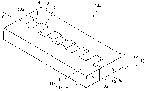
[0027] Fig. 1 is a simplified perspective view representing a wavelength
converter in
Embodying Mode 1 of the present invention.
Fig. 2 is a simplified perspective view representing a wavelength converter in
a
modified example of Embodying Mode 1 of the present invention.
Fig. 3 is a simplified perspective view representing a starting substrate in
Embodying Mode 1 of the present invention.
Fig. 4 is a simplified perspective view representing a situation in which a
crystal
has been grown, in Embodying Mode 1 of the present invention.
Fig. 5 is a simplified perspective view representing a situation in which a
crystal is
sectioned, in Embodying Mode 1 of the present invention.
Fig. 6 is a simplified perspective view representing a crystal having been
sectioned to form a first crystal, in Embodying Mode 1 of the present
invention.
Fig. 7 is a simplified perspective view representing a separate situation in
which a
crystal has been sectioned, in Embodying Mode 1 of the present invention.
Fig. 8 is a simplified perspective view representing a wavelength converter in
Embodying Mode 3 of the present invention.
Fig. 9 is a simplified sectional diagram representing a situation in which
amoiphous crystal has been grown, in Embodying Mode 4 of the present
invention.
CA 02673998 2009-07-27
-7-
DETAILED DESCRIPTION OF THE INVENTION
[0028] Below, a description of modes of embodying the present invention will
be made
based on the drawings. It should be understood that in the following,
identical or
cor-responding parts in the drawings are labeled with identical reference
marks, and their
description will not be repeated.
Embodying Mode 1
[0029] Reference is made to Fig. 1, a simplified perspective view representing
a
wavelength converter of the present embodying mode. To begin with, in the
present
embodying mode the wavelength converter 10a in Fig. I will be described.
t 0 [0030] As indicated in Fig. 1, the wavelength converter 10a in the present
embodying
mode has an optical waveguide 13. The optical waveguide 13 converts the
wavelength of an
incoming beam 101 input into the optical waveguide 13 through one end 13a
thereof, and
outputs an outgoing beam 102 from the optical waveguide 13 through the other
end 13b
thereof.
[0031] The wavelength converter l0a is furnished with a first crystal 11, and
with a
second crystal 12 in which there is essentially no difference in refractive
index from that of
the first crystal 11. The first and second crystals 11 and 12 preferably are
monocrystalline.
[0032] The first and second crystals 11 and 12 form a domain inversion
structure in
which the polar directions along the optical waveguide 13 periodically
reverse. That is, an
optical waveguide 13 for confining light waves is formed in the first and
second crystals 11
and 12 creating the domain inversion structure. The domain inversion structure
satisfies
quasi-phase-matching conditions for the incoming beam 101. Herein,
"quasi-phase-matching conditions" are, given a structure in which, along a
propagation axis
in a nonlinear optical crystal, the sign of the nonlinear optical coefficient
periodically
reverses, the conditions that obtain phase-matching by compensating, with the
wave vector
of the periodic structure, the difference between the wave vector of the
nonlinear domains
and the wave vector of a light wave about to be generated.
[0033] For the first and second crystals 11 and 12 to form the domain
inversion structure,
they are respectively poled in such a way that the direction of the arrow is
positive-polar, for
example. That is, in the present embodying mode, the positive-polar directions
of the first
and second crystals 11 and 12 are opposites. In an implementation in which the
first and
second crystals 11 and 12 are AIN, a first-being the positive-polar-surface 11
a of the first
CA 02673998 2009-07-27
-g-
crystal 11 would be the Al-polar face, while a second-being on the side
opposite from the
positive-polar-surface 12b of the second crystal 12 would be the N-polar face.
[0034] Also, in the optical waveguide 13, with the adjoining first and second
crystals 11
and 12 being single-cycled, the wavelength converter 10a will have a one or
more cycles,
with it preferably having five or more cycles.
[0035] It is preferable that the first and second crystal 11, 12 interfaces
14, which
constitute the optical waveguide 13 and which cross the lengthwise axis of the
optical
waveguide 13, be free of gaps. The poling of the domains reverses at the
interfaces 14. On
the other hand, gaps may be present at the first and second crystal 11, 12
interfaces 15, which
run parallel to the lengthwise axis of the optical waveguide 13.
[0036] The difference in refractive index between these first and second
crystals 11 and
12 is essentially nil. With there being essentially no difference in
refractive index, reflection
of light at the interfaces 14, crossing the lengthwise axis of the optical
waveguide 13 (the
advancing direction of the incoming beam 101), between the first and second
crystals 11 and
12 can be minimized. This makes it possible to reduce losses in the
transmissivity of an
incoming beam 101 passing through the optical waveguide 13. "Essentially no
difference in
refractive index" means that for example if the first and second crystals 11
and 12 are
five-cycled (that is, there are nine interfaces 14 between the first and
second crystals 11 and
12), the difference in refractive index between the first and second crystals
11 and 12 is not
greater than 0.01, and if the first and second crystals 11 and 12 are ten-
cycled, the difference
in refractive index is not greater than 0.001. In such implementations, the
wavelength
converter IOa has a transmissivity of, for example, 90% or greater.
[0037] Herein, the refractive index is value determined, for example,
employing spectral
ellipsometry at a wavelength of 400 to 800 nm by means of a spectral
ellipsometer.
[0038] The first and second crystals 11 and 12 in the present embodying mode
are in a
comb-like form, in which they have regularly arrayed projections on a surface,
and thus are
interdigitated. In other words, the first and second crystals 11 and 12 have
projections and
recesses, with the projections on the first crystal 11 interlocking into the
recesses in the
second crystal 12, and the recesses in the first crystal 11 interlocking with
the projections on
the second crystal 12.
[0039] Furthermore, at least one or the other of the first and second crystals
I 1 and 12 has
a dislocation density of from 1 x 10³ crn Z to less than 1 x 10⁷ cmZ,
preferably of from 1 x
CA 02673998 2009-07-27
-9-
103 cm 2 to less than 1 x 105 cm-2. In the present embodying mode the
dislocation density of
the first and second crystals 11 and 12 is within said range. Being less than
1 x 10⁷ em-2
makes it possible to curtail absorbance of the energy of the incoming beam 101
at
dislocations, so that elevation in the temperature of the first and second
crystals 11 and 12
may be restrained. Use-based degradation in intensity of the outgoing beam 102
can
therefore be curtailed, allowing the lifespan during which the characteristics
are sustainable
to be improved. Being less than 1 x 10' cm 2 enables effective minimization of
incoming-beam 101 energy absorbance at dislocations. While lower dislocation
densities
are preferable, from the perspective of allowing easy manufacture, the lower
limit is 1 X 10³
em Z.
[0040] Herein, the dislocation density is for example a value (etch pit
density, or "EPD")
determined by means of an alkali etching process in which the number of pits
that appear as
a result of etching within molten potassium hydroxide (KOH) is counted and
divided by unit
surface area.
[0041] While the first and second crystals 11 and 12 may differ in chemical
composition,
preferably they are of the same composition. Also, the first and second
crystals 11 and 12
preferably are composed of A1xGa(1_,x)N (0.5 < x< 1). In this case, owing to
the thermal
conductivity when the atomic fraction x of Al is from 0.5 to 1, having the
crystals have the
forgoing dislocation density ensures the result that the lifespan may be
improved will be
demonstrated. Here, the atomic fraction x in AlxGa(i,C)N is the molar ratio of
Al.
[0042] Reference is now made to Fig. 2, a simplified perspective view
representing a
wavelength converter 10b in a modified example of the present embodying mode.
As
indicated in Fig. 2, the geometry of the first and second crystals 11 and 12
where they
interlock may be in a sawtooth form. Moreover, the first and second crystals
11 and 12, not
being particularly limited to geometries such as comb-like or sawtootll, may
have a wavelike
or other geometry.
[0043] To continue, a method of manufacturing a wavelength converter in the
present
embodying mode will be described. Reference is made to Fig. 3, a simplified
perspective
view representing a starting substrate 21 in the present embodying mode. As
indicated in
Fig. 3, the starting substrate 21 is prepared. The starting substrate 21 has a
major surface
21 a. The major surface 21a is for example the (001) plane (c-plane).
CA 02673998 2009-07-27
-10-
[0044] It is preferable that the starting substrate 21 that is prepared have
the same
chemical composition as the crystal 22 that is grown. Preparing a starting
substrate 21
composed of AICGa(i)N (0.5 < x< 1) is also preferable.
[0045] Reference is made to Fig. 4 a simplified perspective view representing
a situation
in which a crystal 22 has been grown in the present embodying mode. Next, as
indicated in
Fig. 4 the crystal 22 is grown onto the major surface 21a of the starting
substrate 21.
[0046] In implementations in which crystal 22 of the same composition as the
starting
substrate 21 is grown, lattice mismatch and the like between the starting
substrate 21 and
crystal 22 is alleviated, thus making it possible to grow crystal 22 of low
dislocation density.
In the present embodying mode, the dislocation density of the growth crystal
22 preferably is
from 1 x 10³ em 2 to less than 1 x 10⁷ em 2, more preferably from 1 x 10³ em Z
to less than 1
x105em2.
[0047] Further, the crystal 22 is grown so as to contact the major surface 21a
of the
starting substrate 21. That is, no mask or other such layer intervenes between
the starting
substrate 21 and the crystal 22. Thereby, crystal 22 poled in such a way that
the direction of
the arrow (the growth front) will be positive-polar is obtained.
[0048] The growth method is not particularly limited; a vapor deposition
process such as
sublimation deposition, hydride vapor-phase epitaxy (HVPE), molecular-beam
epitaxy
(MBE), and metalorganic chemical vapor deposition (MOCVD), or solution
deposition
processes including flux method, and high-nitrogen-pressure growth can be
adopted.
[0049] Reference is now made to Fig. 5, a simplified perspective view
representing a
situation, in the present embodying mode, in which the crystal 22 is
sectioned, and to Fig. 6,
a simplified perspective view representing the crystal 22 having been
sectioned to form a
first crystal 11, in the present embodying mode. Next, as indicated in Figs. 5
and 6, the
crystal 22 is sectioned into two or more in such a way that the domains are
the reverse of
each other, wllereby the first crystal 11 and the second crystal 12 are
formed. Inasmuch as
the first and second crystals 11 and 12 are formed from a single crystal 22,
the chemical
compositions and refractive indices of the first and second crystals 11 and 12
are the same.
[0050] Again, in implementations employing crystal 22 of low dislocation
density, first
and second crystals 11 and 12 that preferably are from 1 x 10³ em Z to less
than 1 x 10⁷ em 2,
more preferably from 1 x 103 cm 2 to less than 1 X 105 cm 2, can be formed.
CA 02673998 2009-07-27
-11-
[0051] In the present embodying mode, as indicated in Fig. 5, the growth front
(major
surface 22a) is sectioned along growth axis so as to be in a comb-like form.
That is, seen
from the major surface 22a of the crystal 22, the first and second crystals 11
and 12 are
sectioned so as to be in comb-like forms.
[0052] When sectioned in this way, the major surface 22a of the crystal 22
forms a first
surface lla of the first crystal 11, and a second surface 12b of the second
crystal 12. The
back side 22b of the crystal 22 on the opposite side from the major surface
22a forms a
second surface 11b of the first crystal 11, and a first surface 12a of the
second crystal 12.
[0053] While the method of sectioning is not particularly limited, a laser or
wire saw can
be employed. Sectioning by means of a laser is advantageous in that it allows
the machining
accuracy to be improved. Employing a wire saw is advantageous in that it
allows costs to be
reduced.
[0054] A first crystal 11 can thereby be formed in which, as indicated in Fig.
6, the
direction heading from the second surface 11 b to the first surface 11 a is
positive-polar.
Likewise, a second crystal 12 in which the direction heading from the first
surface 12a to the
second surface 12b is positive-polar can be formed.
[0055] Reference is made to Fig. 7, a simplified perspective view representing
a separate
situation, in the present embodying mode, in which a crystal 22 has been
sectioned. As
indicated in Fig. 7, the crystal 22 may be sectioned along the growth axis in
such a way that
the growth-front (major-surface 22a) intersecting surface (the surface
paralleling the growth
axis) will be comb-like, to form the first and second crystals 11 and 12.
[0056] Here again, the geometry into which the crystal 22 is sectioned is not
limited to the
comb-like forms depicted in Figs. 5 and 7. The crystal 22 may be sectioned in
such a way
that one of the surfaces will be in a sawtooth geometry, as depicted in Fig.
2. In that case, the
advantage is that the machining is extraordinarily easy.
[0057] Next, at least one surface of the first and second crystals 11 and 12
is etched. The
poling in the at least one surface of the first and second crystals 11 and 12
can thereby be
further guaranteed. The etching may be either wet etching or dry etching.
[0058] For example, if the first and second crystals 11 and 12 are A1N, then
etching in
KOH as a wet etch makes it possible readily to form a face in which the Al
atoms are
terminal, since the etch rate of the N atoms is faster than the etch rate of
the Al atoms.
Meanwhile, reactive ion etching (RIE) as a dry etch, with the one face being a
mask, makes
CA 02673998 2009-07-27
- 12-
it possible readily to form on the other surface a face in which the Al atoms
are terminal. It
should be understood that the etching step may be omitted.
[0059] Next, at least one surface of the first and second crystals 11 and 12
is polished.
The polished surface makes more reliable poling possible. While the polishing
method is
not particularly limited, a process such as chemical mechanical planarization
(CMP), for
example, may be adopted. It should be understood that the polishing step may
be omitted.
Moreover, either the etching step or the polishing step alone may be
implemented, or both
steps may be implemented. Where both are implemented, the polishing step may
be
implemented prior to the etching step.
[0060] Next, the first and second crystals 11 and 12 are put together to form
a domain
inversion structure in which the polar directions of the first and second
crystals 11 and 12
periodically reverse along the optical waveguide 13, and so that the domain
inversion
structure satisfies quasi-phase-matching conditions for the incoming beam 101.
[0061] More specifically, as indicated in Fig. 5 as well as Fig. 7, one alone
of the
sectioned first and second crystals 11 and 12 is reversed 180 , and the comb-
like faces are set
opposite each other. In that state, the first and second crystals 11 and 12
are interlocked.
Inasmuch as the first and second crystals 11 and 12 in the present embodying
mode are
comb-like or saw-toothed, the projections on the first crystal 11 and the
recesses in the
second crystal 12 (the recesses in the first crystal 11 and the projections on
the second crystal
12) are fit into each other. Afterwards, annealing may be carried out to
eliminate any gaps
along the interfaces 14 between the first and second crystals 11 and 12.
[0062] In accordance with the foregoing, as indicated in Fig. 1 as well as
Fig. 2,
wavelength converters l0a and IOb can be manufactured by forming a domain
inversion
structure in which the polar direction along an optical waveguide 13 is
periodically inverted,
wherein the domain inversion structure satisfies quasi-phase matching
conditions for an
incoming beam 101.
[0063] To continue, the functioning of the wavelength converters 10a and lOb
will be
described. Initially, an incoming beam 101 is input through one end 13a of the
optical
waveguide 13 in the wavelength converters l0a and lOb. The incoming beam 101
is
preferably input perpendicular to the poling interfaces 14 in the first and
second crystals 11
and 12. The incoming beam 101 passes through the optical waveguide 13, heading
toward
the other end 13b of the optical waveguide 13. At that time, in the optical
waveguide 13 the
CA 02673998 2009-07-27
- 13 -
phase of the incoming beam 101 is eonverted by the first and second crystals
I1 and 12
having the domain inversion structure satisfying the quasi-phase matching
conditions. An
outgoing beam 102 in which the wavelength has been converted is then output
through the
other end 13b of the optical waveguide 13. An incoming beam 101 of a given
wavelength
can thereby be converted into an outgoing beam 102 of a different wavelength.
[0064] As described in the foregoing, wavelength converters l0a and 10b in the
present
embodying mode are wavelength converting devices having an optical waveguide
13, and
converting the wavelength of an incoming beam 101 input through one end 13a of
the
optical waveguide 13 and outputting an outgoing beam 102 through the other end
13b of the
optical waveguide 13, and are furnished with a first crystal 11, and a second
crystal 12 whose
difference in refractive index from that of the first crystal 11 is
essentially nil. The first and
second crystals I1 and 12 form a domain inversion structure in which the polar
direction
along the optical waveguide 13 is periodically inverted, with the domain
inversion structure
satisfying quasi-phase matching conditions for the incoming beam 101.
[0065] A method of manufacturing the wavelength converters l0a and l Ob in the
present
embodying mode is provided with: a step of growing crystal 22; a step of
forming a first
crystal 11 and a second crystal 12 by sectioning the crystal 22 into two or
more in such a way
that the domains are the reverse of each other; and a step of interlocking the
first and second
crystals 11 and 12 to form a domain inversion structure in which the polar
directions of the
first and second crystals 11 and 12 along the optical waveguide 13
periodically reverse, in
such a way that the domain inversion structure satisfies quasi-phase-matching
conditions for
the incoming beam 101.
[0066] In accordance with a method of manufacturing wavelength converters l0a
and
l Ob in the present embodying mode, the first and second crystals 11 and 12
are formed from
a single crystal 22 by sectioning. Therefore, the refractive index of the
first and second
crystals 11 and 12 is the same. The first and second crystals 11 and 12 are
interlocked to
form the domain inversion structure, and thus when an incoming beam 101 is
transmitted
through the optical waveguide 13, reflection in the optical waveguide 13 at
the interfaces 14
between the first and second crystals 11 and 12 can be minimized. The fact
that
transmissivity losses at the interfaces 14 between the first and second
crystals 11 and 12 may
accordingly be reduced makes it possible to manufacture wavelength converters
l0a and
l Ob in which the transmissivity-as expressed by the intensity, with respect
to the intensity
CA 02673998 2009-07-27
- 14-
of an incoming beam 101 input through the one end 13a of the optical waveguide
13, of an
outgoing beam 102 output tlirough the other end 13b-is improved.
[0067] What is more, the wavelength converters 10a and 10b can be manufactured
by
sectioning the first and second crystals 11 and 12 from the crystal 22,
inverting one and
fitting them together. Wavelength converters l0a and l Ob utilizing first and
second crystals
11 and 12 composed of, for example, AlcGa(i)N (0.5 < x< 1) can therefore
readily be
manufactured.
Embodying Mode 2
[0068] A wavelength converter in the present embodying mode is almost like the
wavelength converters l 0a and I Ob of Embodying Mode 1 represented in Fig. 1
as well as
Fig. 2. Further, the first crystal 11 alone has polarity, while it is
acceptable for the second
crystal 12 not to have polarity.
[0069] To continue, a method of manufacturing wavelength converters l 0a and l
Ob in the
present embodying mode will be described. The wavelength converter l0a and lOb
manufacturing method of the present embodying mode comprises a configuration
basically
like that of Embodying Mode 1, but differs in that a second crystal 12 formed
from the
crystal 22 from which the first crystal 11 is formed is not used.
[0070] Specifically, a starting substrate 21 is prepared in the same manner as
in
Embodying Mode 1. Next, a first crystal 11 (crystal 22) is grown in the same
manner as in
Embodying Mode 1.
[0071] Next, a second crystal 12, having essentially no difference in
refractive index
from that of the first crystal 11, is prepared. In the present embodying mode,
the first crystal
11 depicted in Fig. 6 is formed, and a second crystal 12 that can form a
domain inversion
structure with the first crystal 11 is prepared.
[0072] For the method of preparing the second crystal 12, for example, second
crystals 12
formed from crystal 22 separate from the crystal 22 from which the first
crystal 11 is formed
are prepared by forming pluralities of the first and second crystals 11 and 12
depicted in Fig.
5 or Fig. 7. Alternatively, to prepare the second crystal 12, crystal 22 may
be grown so as not
to have polarity, machined to have a geometry that inter-fits with the first
crystal 11. Here,
the first and second crystals 11 and 12 are of essentially the same chemical
composition; thus
difference in refractive index is essentially nil.
CA 02673998 2009-07-27
-15-
[0073] In this case, the crystal 22 is formed onto a starting substrate 21 of
the same
chemical composition, and thus even though the first and second crystals 11
and 12 are not
formed from the same crystal 22, the dislocation density of the first and
second crystals 11
and 12 can be reduced to from 1 X 103 cm 2 to less than 1 x 107 cm 2.
[0074] Next, in the same manner as in Embodying Mode 1, the first and second
crystals
11 and 12 are interlocked to form a domain inversion structure in which the
polar directions
of the first and second crystals 11 and 12 along the optical waveguide 13
periodically
reverse, in such a way that the domain inversion structure satisfies quasi-
phase-matching
conditions for an incoming beam= 101. Wavelength converters l0a and l Ob of
the present
embodying mode can thereby be manufactured.
[0075] In accordance with a method, as described above, in the present
embodying mode
of manufacturing wavelength converters l0a and lOb, a step of preparing a
first crystal 11,
and a step of preparing second crystal 12 having essentially no difference in
refractive index
from that of the first crystal 11 are provided, and a domain inversion
structure is formed by
interlocking the first and second crystals 11 and 12 whose difference in
refractive index is
essentially nil. Therefore, even with the first and second crystals 11 and 12
being formed
from different crystals 22, reflection in the optical waveguide 13 at the
interfaces 14 between
first and second crystals 11 and 12 when an incoming beam 101 passes through
the optical
waveguide 13 can be minimized. Consequently, transmissivity losses at the
interfaces 14
between the first and second crystals 11 and 12 can be reduced, thus making it
possible to
manufacture wavelength converters l0a and lOb in which the transmissivity is
improved.
[0076] What is particularly advantageous is that poling the first crystal 11
only, forming
the second crystal 12 from another material, and interlocking the first
crystal 11 and the
second crystal 12 allows the wavelength converters l0a and lOb to be
manufactured with
ease.
Enibodying Mode 3
[0077] Reference is made to Fig. 8, a simplified perspective view representing
a
wavelength converter in the present embodying mode. As indicated in Fig. 8, a
wavelength
converter l Od in the present embodying mode comprises a configuration
basically like that
of Embodying-Mode 1 wavelength converter l0a depicted in Fig. 1, but differs
in that the
second crystal is an amorphous crystal 16. There is essentially no difference
in the refractive
index of the amorphous crystal 16 from the refractive index of the first
crystal 11; difference
CA 02673998 2009-07-27
- 16-
from the refractive index of the first crystal 11, at wavelengths from 400 to
800 nm, is
preferably between 0.001 and 0.1.
[0078] In the present embodying mode, the first crystal 11 is preferably
monocrystalline,
and preferably has a dislocation density of from 1 x 103 cm 2 to less than 1 x
107 cm 2.
[0079] In a surface (first surface 11 a) of the first crystal 11, as
illustrated in Figs. 6 and 8,
two or more regularly arrayed projections 11 c and recesses are formed. The
two or more
projections 11c jut out in the same conformation, oriented on lines crossing
the lengthwise
axis of the optical waveguide 13 (the direction along which the incoming beam
101 passes
through the optical waveguide 13). It is preferable that in the projections l
lc the width Wil,
as indicated in Fig. 8, of the sections constituting the wall faces in the
optical waveguide 13
be at least a predetermined size. The predetermined size is, for example, at
least 26 ,um.
Moreover, in the projections it is preferable that the jutting angle B/i be in
the vicinity of 90 .
[0080] The amorphous crystal 16 has projections and recesses in the same
fashion as the
first crystal 11. The recesses in the amorphous crystal 16 couple with the
proj ections 11 c on
the first crystal 11, and the projections on the amorphous crystal 16 couple
into the recesses
in the first crystal 11.
[0081] Now a method of manufacturing a wavelength converter in the present
embodying
mode will be described. To begin with, a starting substrate 21 is prepared in
the same way as
in Embodying Mode 1. Next, a first crystal 11 is grown onto the starting
substrate 21. Then,
two or more regularly arrayed projections are formed in a surface of the first
crystal 11. In
these steps, the crysta122 is grown onto the starting substrate 21, and a
first crystal 11 having
at least two regularly arrayed projections is sectioned from the crystal 22,
in the same way,
for example, as in Embodying Mode 1. A first crystal I 1 as depicted in Fig. 6
can thereby be
formed.
[0082] Reference is made to Fig. 9, a simplified sectional diagram
representing a
situation in which amorphous crystal 16 has been grown in the present
embodying mode.
Next, as indicated in Fig. 9 second crystal, being amorphous crystal 16 whose
difference in
refractive index from that of the first crystal 11 is essentially nil, is
grown onto a surface of
the first crystal 11. In this step, a domain inversion structure in which the
polar directions of
the first and second crystals 11 and 12 periodically reverse along the optical
waveguide 13 is
formed, and the first and second crystals 11 and 12 are formed in such a way
that the domain
inversion structure satisfies quasi-phase-matching conditions for an incoming
beam 101.
CA 02673998 2009-07-27
- 17-
[0083] In the present embodying mode, a second crystal that is amorphous
crystal 16 of
the same chemical composition as the first crystal 11 is grown. Amorphous
crystal 16 of
refractive index that is essentially not different from that of the first
crystal 11 can thereby be
grown. In particular, the amorphous crystal 16 is preferably grown so that its
difference in
refractive index at 400 to 800 nm wavelength from that the first crystal is
from 0.001 to 0.1.
Here, the method whereby the amorphous crystal 16 is grown is not particularly
limited.
[0084] When the amorphous crystal 16 is grown, the polarities of the first
crystal 11 and
the amorphous crystal 16 turn out oppositely oriented. The domain inversion
structure can
therefore be created with ease. This procedure makes it possible to
manufacture the
wavelength converter l Od depicted in Fig. 8.
[0085] In accordance with a method, as described above, in the present
embodying mode
of manufacturing a wavelength converter 10d, amorphous crystal 16 having
essentially no
difference in refractive index from that of the first crystal 11 is grown onto
a surface of the
first crystal 11 as the second crystal. Accordingly, there is essentially no
difference in
refractive index between the first crystal 11 and the amorphous crystal 16 as
the second
crystal. What is more, utilizing the first crystal 11 and amorphous crystal 16
enables
facilitated formation of a poled structure. Therefore, when an incoming beam
101 is
transmitted through the optical waveguide 13, reflection in the optical
waveguide 13 at the
boundary between the first crystal 11 and amorphous crystal 16 can be
minimized.
Consequently, transmissivity losses at the boundary between the first crystal
11 and
amorphous crystal 16 can be reduced, thus making it possible to manufacture a
wavelength
converter 10d in which the transmissivity is improved.
Embodiments
[0086] In the present embodiment, the effect of providing a step of forming a
first crystal
11 and a second crystal 12 by sectioning a crystal 22 into two or more in such
a way that the
domains are the reverse of each other was investigated.
Pr=esent Invention Exanzples 1 and 2
[0087] Wavelength converters in Examples 1 and 2 of the present invention were
manufactured basically following Embodying Mode 1. Specifically, to begin
with, A1N
single-crystal substrates and Alo.SGao55N single-crystal substrates, with the
major surface
22a being the (001) face, were respectively prepared as starting substrates 21
for present
invention Examples 1 and 2.
CA 02673998 2009-07-27
-18-
[0088] Next, crystal 22 of the same chemical composition as the starting
substrates 21
was grown by sublimation deposition onto the starting substrates 21. CMP
polishing was
thereafter carried out on the front side of the crystals 22.
[0089] Next, the crystals 22 were sectioned into at least two, as indicated in
Fig. 7, in
such a way that the domains would be the reverse of each other, to form comb-
like first
crystals 11 and second crystals 12. Thirty-eight each of the first and second
crystals 11 and
12 were formed. Here, in the projections on the first and second crystals 11
and 12, the width
of the sections constituting the wall faces in the optical waveguide 13 (in
the case of the first
crystals 11, the width Wli as indicated in Fig. 8) was rendered 26.6,um.
[0090] Further, the dislocation densities in the obtained first and second
crystals 11 and
12 were respectively characterized by means of molten alkali etching employing
KOH-NaOH (sodium hydroxide). The result was a dislocation density of 1 x 10³
em Z for
the first and second crystals 11 and 12 of present invention Examples 1 and 2.
[0091] Next, the first and second crystals 11 and 12 were alternately 38-cycle
interlocked.
This formed domain inversion structures in which the polar directions of the
first and second
crystals 11 and 12 periodically reverse along ari optical waveguide 13 as
indicated in Fig. 1,
with the domain inversion structure satisfying quasi-phase-matching conditions
for an
incoming beam 101. Wavelength converters l0a of present invention Examples 1
and 2
were thereby manufactured.
Evaluation Results
[0092] With regard to the wavelength converters of present invention Examples
1 and 2, a
beam from an Nd-YAG laser (neodymium: YAG laser) of 1064 nm wavelength was
input as
an incoming beam into the optical waveguide 13 in such a way as to be
perpendicular to the
poling interfaces 14 of the first and second crystals 11 and 12. An outgoing
beam 102 of 532
nm wavelength was output as a result.
[0093] In accordance with the foregoing, the first and second crystals 11 and
12 were
formed from the same crysta122, and thus the refractive index of the first and
second crystals
11 and 12 was the same. It was therefore confirmed that with wavelength
converters of
present invention Examples 1 and 2, an input incoming beam 101 could be
transmitted
through the optical waveguide 13, and extracted as a wavelength-converted
outgoing beam
102.
CA 02673998 2009-07-27
-19-
[0094] While a description of embodying modes and embodiment examples of the
present invention has been undertaken in the foregoing manner, combining the
features of
each of the embodying modes and embodiment examples to suit is contemplated
from the
outset. Furthermore, the presently disclosed embodying modes and embodiment
examples
should in all respects be considered to be illustrative and not limiting. The
scope of the
present invention is set forth not by the foregoing embodying modes but by the
scope of the
patent claims, and is intended to include meanings equivalent to the scope of
the patent
claims and all modifications within the scope.