Note : Les descriptions sont présentées dans la langue officielle dans laquelle elles ont été soumises.
CA 02674125 2009-06-25
OPTOELECTRONIC APPARATUS FOR TRANSMISSION OF AN ELECTRICAL
SIGNAL
The invention relates to an optoelectronic apparatus for
transmission of an electrical signal via, galvanically isolated
by means of a one-piece, translucent, plastic body, an input
current circuit, having at least one optical transmission
element, and an output current circuit, having at least one
optical receiving element.
Such optoelectronic apparatuses, having a transmission element,
a receiving element and, on occasion, a translucent, plastic
body are used, for example, for digital and/or analog signal
transmission between two electrical current circuits
galvanically isolated from one another.
In industrial measurements technology, especially in automation,
and process control, technology, such optoelectronic apparatuses
are applied and required in field devices for galvanic isolation
of the electrical current circuits for explosion protection.
Such field devices ascertain, for example, pressure, flow, fill
level, dielectric constant, surface or interface, temperature or
a some other physical and/or chemical process quantity as
process variable in the conducting of a process. Available from
the assignee are, for example, field devices under the marks,
Cerabar, Deltabar, Deltapilot, Promass, Levelflex, Micropilot,
Prosonic, Soliphant, Liquiphant, Easytemp, which serve primarily
to determine and/or to monitor at least one of the above
referenced process variables of a medium in a container.
The galvanic isolation is applied both in the case of so-called
two conductor devices, which transmit both the power supply
energy and the measurement signal via a single line-pair, as
well as also in the case of four conductor devices, which use
separate line-pairs, one for transmitting the measuring signal
and the other for transmitting the power supply energy.
Examples of such field devices using optocouplers for
galvanically isolated electrical current circuits are described
in US 46 54 771 A and WO 2004/048905 Al.
Optoelectronic apparatuses using optocouplers are described, for
example, in DE 199 20 403 Al and US 6,947,620 B2. In general,
such optoelectronic apparatuses are composed of at least one
transmission element, e.g. a light emitting diode, and at least
one receiving element, e.g. a photodiode or a phototransistor,
which are spatially and galvanically isolated from one another
via at least one light conducting element.
1
CA 02674125 2012-08-29
75089-107
In order that such optoelectronic apparatuses used for the
signal transmission can satisfy the explosion protection
required in industrial measurements and automation technology,
also required are minimum separations between galvanically
isolated, electrical current carrying components, as well as
minimum values for air distances, insulation thicknesses and
electrical current creep paths. Thus, for example, in the case
of a maximum allowable voltage of 250 V, the air distances and
the creep path length between galvanically isolated electrical
current circuits must be at least 10 mm, or the thickness of
solid insulation at least 1 mm. These separations refer, in
such case, especially, to the minimum distances between the
operationally electrical current carrying connections and
conductive traces of the electrical current circuits coupled by
means of such optoelectronic apparatuses. Furthermore, there
are, for such apparatuses serving as optocouplers, increased
requirements also as regards temperature resistance and
explosion endangerment risk, as well as also as regards damage
scenarios accompanying possibly occurring cases of overloading.
In order, in spite of the high safety requirements, to enable
an, as much as possible, high coupling factor, as well as an,
as much as possible, compact form of construction of such
optoelectronic apparatuses, their light conducting elements are
correspondingly embodied to meet the requirements of explosion
protection and signal transmission.
An object of some embodiments is to provide an optoelectronic
apparatus as optocoupler, which is compact, cost¨effective and
simple to manufacture. Furthermore, the optoelectronic
apparatus should provide a high coupling factor, while
2
CA 02674125 2012-08-29
75089-107
fulfilling mechanical requirements and the required explosion
protection requirements.
According to one aspect of the present invention, there is
provided optoelectronic apparatus for transmission of an
electrical signal via, galvanically isolated by means of a one-
piece, translucent, plastic body, an input current circuit,
having at least one optical transmission element, and an output
current circuit, having at least one optical receiving element,
wherein the optical transmission element has a principle
transmission axis of maximum transmission intensity and the
optical receiving element a principle receiving axis of maximum
receiving intensity, wherein the principle transmission axis
and the principle receiving axis coincide with a shared optical
axis, wherein the plastic body has two cavities separated via a
partition for accommodating, respectively, the optical
transmission element and the optical receiving element, wherein
openings of the two cavities in the plastic body lie on the
optical axis, and wherein the transmitting element and/or the
receiving element are/is placed through the openings so far
into the cavities of the plastic body, that, following a case
of overvoltage on the transmitting element and/or the receiving
element, an insulating air distance and creep path according to
an insulation coordination is still present along outer
surfaces of the plastic body.
According to another aspect of the present invention, there is
provided use of the apparatus as described herein as an
optocoupler between galvanically isolated, electrical current
circuits of a field device of process automation technology.
2a
CA 02674125 2012-08-29
75089-107
The aforementioned components, and components described in the
examples of embodiments, as used according to the invention,
are subject to no special conditions as regards their size,
shape, formation, materials and technical designs, so that
selection criteria known in the field of application can be
used without limitation.
2b
õ
CA 02674125 2009-06-25
Other details, features and advantages of the subject matter of
the invention will become apparent from the subsequent
description of the associated drawings, in which preferred
examples of embodiments of the invention are presented. In the
examples of embodiments of the invention shown in the figures,
in order to avoid clutter and for simplification, components or
assemblies of components, which correspond in construction
and/or in function, are provided with equal reference
characters. The figures of the drawings show as follows:
Fig. 1 a first example of an embodiment of the optoelectronic
apparatus of the invention,
Fig. 2 a second example of an embodiment of the
optoelectronic apparatus of the invention,
Fig. 3 a third example of an embodiment of the optoelectronic
apparatus of the invention,
Fig. 4 a first example of application of the optoelectronic
apparatus of the invention as optocoupler.
Fig. 5 a second example of application of the optoelectronic
apparatus of the invention.
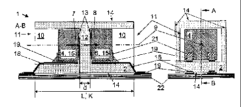
Fig. 1 shows a first example of an embodiment of the
optoelectronic apparatus 1 of the invention for transmission of
an electrical signal S, on the right as side view and on the
left as sectional view according to the cutting plane A-B of the
side view. This optoelectronic apparatus 1 can, for example, be
applied for galvanic isolation of an input electrical current
circuit 3 from an output electrical current circuit 5. The
optoelectronic apparatus 1 is composed essentially of a one-
piece, translucent, plastic body 2, in which, galvanically
isolated via a partition 12, an optical transmitting element 4
in the input current circuit 3 and an optical receiving element
6 in the output current circuit 5 are placed. For this, two,
oppositely lying cavities 10 separated via the partition 12 are
formed in the plastic body 2. Via the openings 11 of the
cavities 10, the optical transmitting element 4 and the optical
receiving element 6 can be emplaced in the plastic body 2.
Electrical contacting occurs via connecting conductors 18, which
are connected via solder connections 19 at contact surfaces 21
on the optical transmitting element 4 and optical receiving
element 6. The connecting conductors 18 are led out of the
cavities 10 to the conductive trace connections on the circuit
3
' CA 02674125 2009-06-25
board 22 and electrically conductingly connected via solder
connections 19. The creep path length L between the connection
conductors 18 on the circuit board 22 or on the outer surface 14
of the plastic body 2 is greater than ten millimeter. Thus,
there results a base length K of the plastic body 2 of somewhat
more than ten millimeters, e.g. eleven millimeter, whereby the
electrical requirements for the optoelectronic apparatus 1
according to German Industrial Standard EN 50020 are met.
Orientation of the transmission element 4 and the receiving
element 6 occurs via the cavities 10 in the plastic body 2. For
example, the cavities 10 slightly conically narrow toward the
faces 13 of the partition. In this way, for example, the
principle transmission axis 7 of the transmission element 4
coincides with the principle receiving axis 8 of the receiving
element 6 along the optical axis 9.
The transmitting element 4 and the receiving element 6 are
constructed in this embodiment as surface mountable components
15, with mounting being on their lateral edges. However, an
application of discrete components or, such as shown in Fig. 3,
of thin film components 16 of an organic, semiconducting
material are other options for examples of embodiments of the
invention.
The faces 13 of the partition 12 are, for example, polished,
whereby an increased direct current, transfer ratio, of about
240, is reached. The direct current, transfer ratio (CTR =
Current Transfer Ratio) states for optocouplers the ratio
between the input signal current to the output signal current.
In the case of optocouplers having a photodiode as receiving
element 6, the direct current, transfer ratio lies in the range
of 0.001-0.005 of the input electrical current, while in the
case of optocouplers having a photo transistor as receiving
element 6, the range is 10-10000. The partition has a thickness
d of at least one millimeter.
A great advantage of this embodiment of the plastic body 2 of
the invention is that, even after an explosion of the
transmission element 4 or of the receiving element 6 due to a
supplying of the components with a high voltage, e.g. 250 volt,
no creep path can occur over the outer surfaces 14 of the
plastic body 2 or the circuit board 22. The arising metal
vapors are, due to the embodiments of the cavities 10 of the
invention, expelled from the openings 11 in different
directions, so that no metal fog can deposit. Furthermore, the
pressure wave of an exploding transmission element 4 or
4
CA 02674125 2009-06-25
receiving element 6 directed toward the openings 11 in the
plastic body 2 has scarcely any mechanical effect on the plastic
body 2 itself, so that it is not destroyed. Therefore, even a
thickness d of the partition 12 of a millimeter can be
sufficient to resist the possibly arising, pressure wave. Since
short circuit resistance is also assured after an explosion of
the components, the placing of fuses before the transmission
element 4 or the receiving element 6 for limiting power uptake
can be omitted, which leads to a considerable space saving on
the circuit board 22.
Fig. 2 shows a second example of an embodiment of the
optoelectronic apparatus 1 of the invention for transmission of
an electrical signal S, on the right as side view and on the
left as sectional view according to the cutting plane C-D of the
side view. In contrast to the first example of an embodiment in
Fig. 1, here in the plastic body 2, the partition 12 is embodied
as an optical filter 17. For this, for example, a filter
element is present during, and locked in place by, the injection
molding manufacture of the plastic body 2. This optical filter
17 has the function of passing only the wavelength, e.g.
infrared light, of the transmission element 4, while background
light irradiation is blocked. The optical filter 17 can, for
example, be embodied as an interference filter, in the form of a
high quality, optical filter, having a narrow transmissive range
and a high degree of suppression in the blocking region. This
optical filter 17 can also be embodied by application of a
filter film to the faces 13 of the partition 12 or directly on
the transmission element 4, or receiving element 6.
Furthermore, Fig. 2 shows another method of contacting the
transmission element 4 and the receiving element 6. For this,
the plastic body 2 was partially coated with a metal or thin
metal layers were applied as connecting conductor 18 on the
surface of the plastic body 2 in the cavities 10. The
connecting conductors 18 are led a segmental width on the outer
surface 14, so that they can be connected with conductive traces
on the circuit board 22.
Another type of manufacture of connection conductors is provided
by MID technology (Moulded Interconnected Devices). In such
case, either a core-catalytically filled, metallizable plastic
is so modified in ascertained regions by a laser, that,
partially, a metal layer can be galvanically deposited or, in
the case of a large-surface, metallized, plastic body 2, a laser
is used to partially vaporize the metal layer and, thus, to form
the connecting conductor 18.
CA 02674125 2009-06-25
The electrical connection between the connection conductors 18
and contact surface 21 of the transmission element 4, or
receiving element 6, as well as to the conductive traces, occurs
by means of an electrical, adhesive connection 20.
Fig. 3 shows a third example of an embodiment of the
optoelectronic apparatus 1 of the invention for transmission of
an electrical signal S, on the right as side view and on the
left as sectional view according to the cutting plane E-F of the
side view. In this example of an embodiment, two thin-film
components 16 of an organic, semiconducting material are adhered
directly to the faces 13 of the partition 12 by means of an
optical adhesive. Advantage of this example of an embodiment
lies in the fact that the connecting conductor 18 can be adhered
with large area of contact on the rear of the thin-film,
transmission element 4 or receiving element 6 by means of an
electrically conductive, adhesive connection 20, whereby a
simple mounting of the optoelectronic element 1 is provided.
Fig. 4 shows a first example of application of the
optoelectronic apparatus 1 of the invention as optocoupler for
transmission of an alternating voltage signal. The input
current circuit 3 comprises a signal generator 33, which feeds,
limited via a resistor 30, a light emitting diode 25 as
transmission element 4. Light-emitting diode 25 sends,
corresponding to the signal of the signal generator, a light
signal to the receiving element 6 in the output current circuit
5. The output current circuit 5 comprises a phototransistor 24
as receiving element 6, whose output signal is amplified by a
non-inverting, operational amplifier circuit. The non-
inverting, operational amplifier circuit is composed of an
operational amplifier 23 and a number of resistors 30 for
setting the amplification.
Fig. 5 shows a second example of application of the
optoelectronic apparatus of the invention as optocoupler for
transmitting the control signal of an AC/DC-converter or DC/DC-
converter. The input current circuit 3 comprises a control
(open, or closed, loop control) unit 27, a field effect
transistor 26 and a first winding of a transformer 21. The
output current circuit comprises a capacitor 29 and a diode 28.
The optoelectronic apparatus measures in the output current
circuit 5 the output voltage Uo, in that this voltage lies
across the light emitting diode 25, so that the light emitting
diode 25 glows in proportion to the output voltage Uo. The
phototransistor 24 as receiving element 6 operates in accordance
6
CA 02674125 2009-06-25
with the light signal. The control unit 27 measures the current
from the phototransistor 24 and controls via the field effect
transistor 26 the energy induced in the transformer 21 for the
input voltage Ui.
7
CA 02674125 2009-06-25
List of Reference Characters
1 apparatus
2 plastic body
3 input current circuit
4 transmission element
output current circuit
6 receiving element
7 principle transmission axis
8 principle receiving axis
9 optical axis
cavity
11 opening
12 partition
13 faces
14 outer surface
surface mountable component
16 thin film component
17 optical filter
18 connecting conductor
19 solder connection
electrical adhesive connection
21 contact surface
22 circuit board
23 OPAmp
24 phototransistor
light emitting diode
26 field effect transistor
27 control unit
28 diode
29 capacitor
resistor
31 voltage supply
32 transformer
33 signal generator
= Electrical signal
Si input signal
So output signal
= base length
= creep path length
= thickness
Ui input voltage
Uo output voltage
8