Note : Les descriptions sont présentées dans la langue officielle dans laquelle elles ont été soumises.
CA 02674337 2015-11-25
75873-7
A CHEMICALLY ENERGIZED SOLID STATE GENERATOR
FIELD
[0001] The field of the invention relates generally to energy conversion
systems and more
particularly relates to a method and system for using pre-equilibrium
ballistic charge carrier
refraction.
BACKGROUND
[0002] The use of solid state junctions to convert ballistic charge carrier
motion directly into
=
electricity has recently been demonstrated in several novel methods and
approaches. As shown
in cross section in Figure 1-A, in each case a charge carrier, most often an
electron, is energized
on or near a conducting surface 10A by an energizer 12A, such as chemical
reactions with or
without using conducting catalysts, using photovoltaic energizing materials,
or using heat
combined with a thermal gradient. In each case the charge carrier
ballistically moves from a
conductor 10A into a semiconductor or dielectric 11A. The conductor 10A is so
thin that the
electron effectively travels through it ballistically, without loosing energy
or colliding with
another electron or atom. The result is a voltage 14A across positive terminal
17A and negative
terminal 16A. In Figure 1-A, the dielectric junction 15A is a semiconductor
junction
specifically chosen to create an electrical potential voltage barrier which
tends to impede the
electron ballistic motion, shown as 11B in Figure 1-B. Figure 1-B shows the
electrical
potential in the device as a function of distance along the device. As shown
in Figure 2-A,
electrons 21A at the conductor surface 22A have an energy greater than the top
of the potential
voltage barrier. These electrons 21A cross over the voltage barrier and lose
energy to heat 24A
before they settle down to the semiconductor conduction band 25A, which
separates the charge
across the conductor-dielectric junction. Electrons traveling against a
potential voltage barrier
convert some of the ballistic electron kinetic energy into electrical
potential energy 27A. The
rest of the ballistic electron kinetic energy becomes heat 24A. The voltage
27A developed is
the difference between the Fermi level of the conductor on one side 28A and
the Fermi level of
the dielectric conductor electrode on the other side 26A. A voltage, V
(Volts), is developed
when the charges separate.
[0003] In a prior art, when energetic chemicals adsorbed on a thin conductor
surface, electrons
with energies greater than a voltage barrier of about 0.5 eV were detected in
sensors similar to
those represented by Figure 1-A, 1-B and 2-A. However, the energy distribution
decreased
exponentially beyond ¨ 0.1 eV, rendering the effect not useful for energy
conversion and
generation. Further, in those sensors the effective electron mass of the metal
conductor 10A, of
order 1 me, is much greater than the effective electron mass in the
semiconductor 11A,
1
CA 02674337 2013-03-21
53965-47
typically silicon, of order 1/3 m_e. This results in most of the generated
electrons being
reflected away from the semiconductor metal interface 15A, and therefore not
collected. The
relevance or utility of the role of electron effective mass has not been
disclosed or expanded.
The scheme also required the cryogenic cooling of the diode to reduce thermal
noise. The
efficiency of this scheme is so low that current can only be measured in the
short circuit mode.
The system can only be used as a chemical sensor and is not a useful electric
generator.
[0004] In a prior system, association reactions on or near a conducting
catalyst surface
energized and initialized highly vibrational excited molecules. The energy of
the vibrationally
excited molecules was transferred to the electrons in the conductor. The
electron energy was
apparently in excess of a 1.2 volt barrier 11B. When a wide bandgap oxide
semiconductor,
TiO2 was used, useful short circuit currents at temperatures well exceeding
the boiling point of
water, (up to 473 Kelvin) are observed. Useful open circuit forward voltage
was observed
under conditions of almost zero temperature gradient at room temperature. The
forward voltage
was similar to that observed in a photovoltaicaly energized system using the
same oxide
semiconductor.
[0005] It would be highly advantageous to use a fabrication method resulting
in predictable
high output voltages and currents, and to be able to choose materials other
than Ti02, to
operate such a converter at an elevated temperature and to generate
electricity in devices of this
type using thermal gradients.
[0006] The field of solid state thennionics uses thermal gradients to energize
charge carriers
and uses semiconductor bandgap engineering to provide voltage barriers across
semiconductor
junctions. In such devices, charge carriers must travel ballistically through
the dielectric 11A.
No charge carrier ballistic travel is required in the material 10A. Moreover,
it is acknowledged
that charge carriers travel in all directions from material 10A towards the
dielectric 11A. The
effects of a step increase in the carrier effective mass during ballistic
transport has not been
used to enhance conversion efficiency and lower fabrication costs.
[0007] All known related converter concepts suffered an inefficiency directly
related to the
unspecified and therefore uncontrolled relative charge carrier effective
masses of junction
materials used. Nowhere does the field claim nor profess to claim any method
or knowledge of
tailoring or controlling carrier effective masses to enhance energy conversion
efficiency.
2
CA 02674337 2014-12-19
53965-47
SUMMARY
[0008] A method and system for using pre-equilibrium ballistic charge carrier
refraction are
disclosed.
[0008a] According to an aspect of the present invention, there is provided an
apparatus,
comprising: one or more solid-state electric generators, the solid-state
electric generators
including at least one chemically energized solid-state electric generator;
wherein the one or
more solid-state electric generators include, a first region of a solid-state
junction, the first
region including a first material having a first charge carrier effective
mass; a second material
of the solid-state junction, the second material having a second charge
carrier effective mass
= 10 greater than the first charge carrier effective mass, wherein a charge
carrier effective mass
ratio between the second charge carrier effective mass and the first charge
carrier effective
mass is greater than or equal to two; and a heat sink connected to the second
material, the heat
sink having a heat sink temperature higher than an ambient temperature and
being configured
to remove heat from said one or more solid-state electric generators; wherein
the one or more
solid-state electric generators are configured to use an interaction of
chemically energized
= reactants to energize a charge carrier in the first material, to have an
effective carrier
temperature higher than a second material temperature of the second material;
wherein the
first material permits ballistic transport of the charge carrier through the
first material and into
the second material.
[0008b] According to another aspect of the present invention, there is
provided an
apparatus, comprising: one or more solid-state electric generators, the solid-
state electric
generators including at least one chemically energized solid-state electric
generator; wherein
the one or more solid-state electric generators include: a solid-state
junction comprised of a
first material layer and a second material layer, wherein the first material
layer comprises a
nanoscopic cluster and is over the second material but maintains sufficient
contact with the
second material, the second material being porous, to form a solid-state
electric generator;
wherein the one or more solid-state electric generators use an interaction of
chemically
energized reactants to energize a charge carrier between the first and second
material.
2a
CA 02674337 2015-11-25
75873-7
[0008c] According to another aspect of the present invention, there is
provided a chemically
energized solid-state electric generator comprising: a solid-state junction
comprising a first
material layer and a second material layer, wherein the first material layer
comprises a
nanoscopic cluster and is over the second material but maintains sufficient
contact with the
second material, the second material being porous, to form a solid-state
electric generator; and
wherein the chemically energized solid-state electric generator uses an
interaction of
chemically energized reactants which energizes a charge carrier between the
first and second
material.
[0008d] According to another aspect, there is provided an apparatus,
comprising: one or
more solid-state electric generators, the solid-state electric generators
including at least one
thermally energized solid-state electric generators; wherein the one or more
solid-state electric
generators include, a first region of a solid-state junction, the first region
including a first
material having a first charge carrier effective mass; a second material of
the solid-state
junction, the second material having a second charge carrier effective mass
greater than the
first charge carrier effective mass, wherein a charge carrier effective mass
ratio between the
second charge carrier effective mass and the first charge carrier effective
mass is greater than
or equal to two; one or more third materials in the first region electrically
in contact with the
first material and not in contact with the second material; a heat source in
thermal contact with
the one or more third materials; and a heat sink connected to the second
material, the heat sink
having a heat sink temperature higher than an ambient temperature; wherein the
one or more
solid-state electric generators are configured to energize a charge carrier in
the first material,
to have an effective carrier temperature higher than a second material
temperature of the
second material; wherein the first material permits ballistic transport of the
charge carrier
through the first material and into the second material.
[0008e] According to another aspect, there is provided a method comprising:
providing one
or more solid-state electric generators including, generating a first region
of a solid-state
junction including a first material having a first charge carrier effective
mass; generating a
second material of the solid-state junction, the second material having a
second charge carrier
effective mass greater than the first charge carrier effective mass, wherein a
charge carrier
2b
CA 02674337 2014-12-19
53965-47
effective mass ratio between the second charge carrier effective mass and the
first charge
carrier effective mass is greater than or equal to two; connecting a heat sink
to the second
material, the heat sink having a heat sink temperature higher than an ambient
temperature; the
first material permits ballistic transport of a charge carrier through the
first material into the
second material; and retarding transport of a charge carrier from the first
material to the
second material with an electrical potential barrier that permits the charge
carrier to traverse
into the second material.
[0008f] According to another aspect, there is provided an apparatus,
comprising: one or
more solid-state electric generators, the solid-state electric generators
including one or more
solid-state electric generators energized by electromagnetic radiation,
including one or more
of evanescent and propagating radiation; wherein the one or more solid-state
electric
generators include, a first region of a solid-state junction, the first region
including a first
material having a first charge carrier effective mass; a second material of
the solid-state
junction, the second material having a second charge carrier effective mass
greater than the
first charge carrier effective mass, wherein a charge carrier effective mass
ratio between the
second charge carrier effective mass and the first charge carrier effective
mass is greater than
or equal to two; and a heat sink connected to the second material, the heat
sink having a heat
sink temperature higher than an ambient temperature; wherein the one or more
solid-state
electric generators have an effective carrier temperature higher than a second
material
temperature of the second material; wherein the first material permits
ballistic transport of the
charge carrier through the first material and into the second material.
[0008g] According to one embodiment, a device comprises one or more solid-
state electric
generators. The solid-state electric generators include one or more from the
group including a
2c
CA 02674337 2009-07-02
WO 2008/085757 PCT/US2007/088972
chemically energized solid-state electric generator and a thermionic solid-
state electric
generator. A first material having a first charge carrier effective mass is
used in a solid-state
junction of a solid-state electric generator. A second material having a
second charge carrier
effective mass greater than the first charge carrier effective mass forms the
solid-state junction.
A charge carrier effective mass ratio of the second effective mass divided by
the first effective
mass is greater than or equal to two.
[0009] The above and other preferred features, including various novel details
of
implementation and combination of elements, will now be more particularly
described with
reference to the accompanying drawings and pointed out in the claims. It will
be understood
that the particular methods and systems described herein are shown by way of
illustration only
and not as limitations. As will be understood by those skilled in the art, the
principles and
features described herein may be employed in various and numerous embodiments
without
departing from the scope of the teachings herein.
BRIEF DESCRIPTION OF THE DRAWINGS
[0010] The accompanying drawings, which are included as part of the present
specification,
illustrate the presently preferred embodiment and together with the general
description given
above and the detailed description of the preferred embodiment given below
serve to explain
and teach the principles of the present teachings.
Figure 1-A illustrates a prior art solid-state electric generator.
Figure 1-B illustrates a prior art graph of potential versus distance and
indicating the effect of a
voltage barrier in a solid-state junction.
Figure 1-C illustrates a graph of potential versus distance in an exemplary
solid-state electric
generator having a Schottky barrier.
Figure 1-D illustrates a graph of potential versus distance in an exemplary
solid-state electric
generator having a p-n junction potential barrier.
Figure 1-E illustrates a graph of potential versus distance in an exemplary
solid-state electric
generator having a conductor-dielectric-conductor nanocapacitor potential
barrier.
Figure 2A illustrates a prior art graph of potential versus distance,
indicating the effect of heat
in an energy conversion process.
Figure 2-B illustrates a graph of potential versus distance in an exemplary
solid-state electric
generator where electrons experience energy loss to heat.
Figure 2-C illustrates a graph of potential versus distance in a solid-state
electric generator
where heat re-energizes electrons to leak back across the junction.
3
CA 02674337 2009-07-02
WO 2008/085757 PCT/US2007/088972
Figure 2-D illustrates a graph of potential versus distance in an exemplary
solid-state electric
generator with a heat sink.
Figure 3-A illustrates an exemplary diagram of potential versus distance in a
region where a
pre-equilibrium ballistic charge carrier moves from a region of low charge
carrier effective
mass into a region of high charge carrier effective mass.
Figure 3-B illustrates an exemplary diagram of a single pre-equilibrium
ballistic charge carrier
refracted into a concentrated angle of travel across a junction
Figure 3-C illustrates an exemplary diagram of multiple pre-equilibrium
ballistic charge
carriers refracted into a concentrated angle of travel.
Figure 3-D illustrates an exemplary diagram of multiple charge carriers
reflected back towards
the junction.
Figure 4 illustrates an exemplary solid state electric generator using diode
pre-equilibrium
energy converter with pre-equilibrium ballistic refraction and heat rejection.
Figure 5 illustrates an exemplary solid-state, in-series, chemically energized
pre-equilibrium
electric generator, according to one embodiment of the present invention.
Figure 6 illustrates exemplary electrically and thermally stacked thermal
gradient converters
using pre-equilibrium energy converters with ballistic refraction.
Figure 7 illustrates an exemplary cross section of a pillar structure on which
pre-equilibrium
ballistic refraction converters are attached.
Figure 8 illustrates an exemplary cross section of a generalized pillar
structure that includes
multiple forms such as corrugations, channels, pores and holes on which
ballistic refraction
converter assemblies are affixed.
Figure 9 illustrates an exemplary cross section showing reactant and coolant
flow from coldest
(inside of structure) to hottest (outside of structure) on which pre-
equilibrium ballistic
refraction converter assemblies are affixed.
Figure 10-A illustrates an exemplary cross section showing inert spacers
formed along with
ballistic refraction converter assemblies on a supporting substrate.
Figure 10-B illustrates an exemplary cross section detail of a spacer and
ballistic refraction
converter assemblies on a supporting substrate.
Figure 11 illustrates an exemplary cross section showing stacking of
substrates containing
ballistic refraction converter assemblies and showing reactant, cooling and
exhaust flows in the
spaces between stacked elements.
4
CA 02674337 2009-07-02
WO 2008/085757 PCT/US2007/088972
Figure 12 illustrates an exemplary cross section showing pre-equilibrium
ballistic refraction
converter assemblies connected electrically in series across the surface of a
supporting
structure.
Figure 13 illustrates an exemplary cross section showing a substrate with
reactant and coolants
flowing through a supporting structure and around ballistic refraction
converter assemblies on
the structure.
Figure 14 illustrates an exemplary cross section of clusters electrically
connected
predominantly by tunneling and physically separated on an energy converter.
Figure 15 illustrates an exemplary addition of materials useful to manage
thermal conductivity
issues into a low charge carrier effective mass region.
Figure 16-A illustrates an exemplary device with minimal or no barrier in the
first material and
an increasing charge carrier effective mass.
Figure 16-B illustrates an exemplary device with minimal or no barrier in the
first material and
the middle material having the lowest charge carrier effective mass.
Figure 16-C illustrates an exemplary device with a barrier in the first
material and an increasing
charge carrier effective mass.
Figure 16-D illustrates an exemplary device with potential barriers against
charge transport in
both directions, and a minimum charge carrier effective mass in the middle
material.
Figure 17 illustrates an exemplary cross section of catalytic accelerators on
pillars, thermally
isolated nanoscopically and near active surface of ballistic refraction
converter assemblies on a
support structure.
Figure 18 illustrates an exemplary surface containing ballistic refraction
converters and spacers
being rolled, permitting reactant and coolant flow through the roll.
DETAILED DESCRIPTION
[0011] Methods, devices and systems for using pre-equilibrium ballistic charge
carrier
refraction are disclosed. According to one embodiment, a method comprises
fabricating one or
more solid-state electric generators. The solid-state electric generators
include one or more
chosen from the group including a chemically energized solid-state electric
generator and a
thermionic solid-state electric generator. A solid state electric generator
energizes a pre-
equilibrium energy distribution of charge carriers in a first material having
a first charge carrier
effective mass and forming a solid-state junction with a second material. The
second material
has a second charge carrier effective mass greater than the first charge
carrier effective mass. A
charge carrier effective mass ratio of the second effective mass divided by
the first effective
mass is greater than or equal to two.
CA 02674337 2015-11-25
75873-7
[0012] In the following description, for purposes of explanation, specific
nomenclature is set
forth to provide a thorough understanding of the various inventive concepts
disclosed herein.
However, it will be apparent to one skilled in the art that these specific
details are not required in
order to practice the various inventive concepts disclosed herein. Some
embodiments of the
present methods, devices and systems improve the energy conversion efficiency
of junctions used
in solid-state devices to generate electricity. An energy source creates an
unbalanced, pre-
equilibrium energy distribution of charge carriers, e.g. electrons, on one
side of a junction. When
a net excess of charge carriers travel ballistically and surmount an
electrical potential barrier upon
crossing from one side of a junction to the other, some of the charge carrier
kinetic energy
associated with motion is directly converted into an electrical potential
energy. Charge separation
occurs and the regions form a capacitor. In the absence of tunneling, only the
velocity component
close to the normal to the potential barrier contributes to surmounting the
barrier.
[0013] The result is the conversion of some pre-equilibrium distribution of
energy into the
useful form of an electrically charged capacitor. A key element of the
embodiments, the
efficiency of this process is improved when the directions of the charge
carriers are refracted to
travel substantially normal to the electrical potential by providing a
material with an abrupt
increase in the carrier effective mass across the junction. Carriers
ballistically traveling
backwards, from high to low charge carrier effective mass regions may
experience total internal
reflection if they approach the junction from any angle greater than a
relatively small critical
= angle. Backward flow tends to drain the separated charges.
[0014] Energizing methods which cause a higher effective charge carrier
temperature in a
material with low charge carrier effective mass compared to the temperature of
the high charge
carrier effective mass region define a non-isothermal charge carrier
distribution, and include
transient, pre-equilibrium distributions of charge carriers. Energizing
methods include using
chemical reactions, using photovoltaic methods, using propagating and/or
evanescent
electromagnetic radiation, using electric coulomb coupling, using heat flow
and associated
thermal gradients, using solar energizers, using heat sources such as
geothermal, friction, and
nuclear heat sources, using nuclear energizing, using in-situ ionizing
radiation, using
radioactive waste radiation, using flame heaters and catalytic heaters, using
piezo-electric
energizing and initializing highly vibrationally excited reaction products
using energetic
chemical reactions.
[0015] According to one embodiment, the present system improves energy
conversion
efficiency by adding a charge carrier effective mass element. The element
includes a
nanoscopic ballistic carrier refraction effect inherent in ballistic charge
transport from a region
of lower charge carrier effective mass into a region of higher charge carrier
effective mass.
6
CA 02674337 2009-07-02
WO 2008/085757 PCT/US2007/088972
[0016] The ratio of the charge carrier effective masses (m_e_high / m _ e_
low) determines the
degree to which the ballistic charge carrier gets refracted towards the
potential barrier. This
ballistic refraction maximizes the charge carrier velocity component towards
and directly
against the potential barrier and minimizes the other charge carrier velocity
components
transverse to the barrier. Minimizing the other components minimizes energy
losses. Ballistic
transport is assured when the lower charge carrier effective mass region is
thin enough to be
transparent to charge carrier motion. The lower charge carrier effective mass
region forms a
nano-layer electrode of the capacitor. The junction of the low and high charge
carrier effective
mass regions forms a capacitor, which stores electrical potential energy as
separated charges.
The material with higher carrier effective mass is the dielectric of the
capacitor.
[0017] According to another embodiment, heat transport across the junction is
minimized.
Ballistic refraction and a junction electrical potential barrier reflect heat-
carrying charge
carriers away from the junction. In the low charge carrier effective mass
region, carriers with
energy less than the barrier potential are reflected back into the hotter
region from whence they
came. In the high charge carrier effective mass side, carriers approaching the
junction with
angles greater than the relatively small critical angle (relative to the
surface normal) are
reflected and can not travel backwards to the low charge carrier effective
mass side.
[0018] Additional embodiments connect nanoscopic thermal gradient converters
thermally in
parallel and/or in series and connect them electrically in parallel and/or in
series. The connected
converters are further connected in parallel and/or in series. The thermal
connections can be
physically distinct from the electrical connections. The energy and heat
sources include those
with unique, spatially non-uniform temperature profiles, temporally sporadic
and non-constant
energy bursts, and various regions may present non-uniform heat flow rates.
[0019] According to one embodiment, a secondary energy conversion process is
used to extract
electrical work by operating a solid state thermionic/thermoelectric heat
engine between a
higher temperature, such as reject heat from a primary energy conversion
process, and the
colder temperature heat sink of the ambient surroundings. Efficiency is
enhanced by using pre-
equilibrium ballistic charge carrier (e.g. electron) refraction (PEBCCR). Heat
engine device
components utilizing PEBCCR are nanoscopic thermal gradient converters (NTGC).
Stacking
nanoscopic thermal gradient converters in series thermally and electrically
provides an efficient
way to implement a heat engine.
[0020] According to one embodiment, a system has successive converter units
one on top of
the other, each converter unit having (a) conductor electrode, (b) low charge
carrier effective
mass region (also referred to as a nano-layer electrode or nano-electrode),
(c) high charge
carrier effective mass region (also referred to as the dielectric) and (d)
conductor electrode.
7
CA 02674337 2015-11-25
One preferred embodiment of this nano-electrode capacitor system forms element
(b) from
conductors such as metals that have relatively long carrier mean free paths,
such as Cu, Ag, Au,
Al; forms material (c) using oxidized Ti metal to create n-type Ti02; and
forms material (a) and
(d) from unoxidized Ti. Another embodiment includes a heavily doped n-Si layer
between the
conductor electrode (a) and the nano-layer electrode (b). Another embodiment
forms the
element (b) using a heavily doped semiconductor such as n-Si or SiGe alloy.
The electrical
barrier of this junction is formed by the band offsets, which are
approximately 0.1 eV. This
favors operation at the maximum power density. Another embodiment includes a
heavily
doped n-Si layer between the high charge carrier effective mass region (c) and
the conductor
electrode (d).
[0021] According to one embodiment, the thickness of the region of lower
charge carrier
effective mass is formed so thin that the carriers effectively travel
predominantly ballistically.
The lower charge carrier effective mass region is formed with one or more
materials with a
lower thermal conductivity relative to electrical conductivity over nanoscopic
dimensions.
Materials with a favorable, enhanced, or high ZT thermoelectric figure of
merit, values of ZT
greater than approximately 0.05, are generally considered to be at least
favorable. The region
including the lowest charge carrier effective mass material with the other
materials is referred
to generally as low charge carrier effective mass region.
[0022] Some embodiments of the methods and systems may be used as a cooler or
refrigerator upon
application of a potential across the junction. The addition of PEBCCR
increases both the cooling
efficiency and the cooling rate. The methods and systems may be also be used
to alter reaction rates.
[0023] One embodiment uses three-dimensional constructs and methods for
tailoring heat
transfer, cooling and power density and for increasing the active area per
volume (volumetric)
to enhance the performance made possible by ballistic carrier refraction.
[0024] According to one embodiment, using pre-equilibrium ballistic charge
carrier refraction
enhances energy conversion efficiency in solid state electric generators. The
embodiment
includes a ballistic charge carrier transport from a region of lower charge
carrier effective mass
into a region of higher charge carrier effective mass. A ratio of high to low
charge carrier
effective mass in excess of approximately 2 provides desirable performance
enhancement. An
absolute high effective carrier mass in excess of approximately 2 will
generally provide
acceptable performance enhancement. The junction region materials are chosen
such that a
surmountable electrical potential is formed for charge carriers traveling from
the low charge
carrier effective mass side to the high charge carrier effective mass side.
Any pre-equilibrium
effective temperature gradient of charge carriers across the junction enables
the energy
conversion.
8
CA 02674337 2009-07-02
WO 2008/085757 PCT/US2007/088972
[0025] Several configurations utilizing PEBCCR include devices energized by
the products of
chemical reactions, surface chemical reactions, interactions with highly
vibrationally excited
molecules, thermal gradients, all forms of electromagnetic coupling such as
propagating and/or
evanescent radiation, in-situ energizing by nuclear radiation, or other
methods.
Pre-Equilibrium Ballistic Charge Carrier Refraction Process (PEBCCRP)
[0026] One embodiment of the present teachings uses a combination of a step
increase in the
charge carrier (electron or hole) effective mass at a material junction and an
electrical potential
barrier at the junction which tends to retard the charge carrier from
traveling into the junction,
as shown generally in Figures 3-A thru 3-D. The step increase in the charge
carrier effective
masses refracts the direction of ballistic travel towards the normal to the
surface junction.
Velocity components transverse to the normal are therefore diminished. In the
solid state, these
effects occur in the nanoscopic regime where transport is ballistic and the
dimensions are less
than the charge carrier mean free path, typically ¨ 1-50 nm and preferably >
¨1 nm. Thickness
dimensions greater than 1 nm can be acceptable. Thicknesses greater than 4 nm
are desirable.
This is referred to as the pre-equilibrium ballistic charge carrier refraction
process (PEBCCRP).
Devices or device components based on PEBCCRP that convert thermal gradients
to electrical
potential are referred to as nanoscopic thermal gradient converters (NTGC).
[0027] For example, as in Figure 3-B, an electron crossing from a region of
low to a region of
high electron effective mass changes direction towards the normal to the
region of higher
electron effective mass. This is equivalent to the Snell's law effect on light
when traveling
from a region of low index of refraction (air) to a region of high index of
refraction (water or
glass), and the governing equations are the same.
[0028] One embodiment provides ballistic carrier refraction. Electrons
generally move in all
directions in a material. Electrons in the low electron effective mass
material approaching the
interface ballistically from any approaching direction all find themselves
traveling nearly
entirely forward with a restricted range of angles into the region of higher
electron effective
mass, as shown in Figure 3-C. Electrons in the high electron effective mass
material
ballistically moving backwards into the region of lower electron effective
mass are reflected
and can not move back unless they approach with angles restricted inside the
critical angle, as
shown in Figure 3-D.
9
CA 02674337 2009-07-02
WO 2008/085757 PCT/US2007/088972
Recursive Pre-Equilibrium Ballistic Charge Carrier Refraction (R-PEBCCR)
[0029] One embodiment provides a method to recursively connect PEBCCRP and/or
nanoscopic thermal gradient converter (NTGC) units where one end of the
recursive system is
the hottest and the other end of the recursive system is the coldest and
attached to a heat sink.
Connecting PEBCCRP and/or nanoscopic theimal gradient converter (NTGC) units
allows
conversion of the heat flow at a higher temperature of a previous PECCRP unit
in the recursive
system to an electrical potential.
Charge Carrier Effective Mass Discontinuity for Chemically Energized Pre-
Equilibrium
Electric Generators.
[0030] To enhance the energy conversion efficiency of chemically energized pre-
equilibrium
electric generators, one embodiment of the teachings uses the carrier
effective mass
discontinuity principle in choosing the material for the junction of lower
charge carrier
effective mass region with dielectric and electrical potential barrier higher
charge carrier
effective mass region. The conductor material is chosen such that its charge
carrier effective
mass is as low as possible compared to the dielectric material whose charge
carrier effective
mass is as high as material choices permit.
Thermal or Heat Rectifier
[0031] One embodiment provides a form of thermal isolation and the resemblance
to heat
rectification. Almost all of the thermal conductivity in most conductors is
associated with
(charge carrier) electron flow, not with phonon or lattice vibrations. The
ballistic charge carrier
refraction permits charge carriers approaching from the low charge carrier
effective mass side
material to transport electrical energy, and hence heat, directly into the
high charge carrier
effective mass side material. The total internal reflection in the high charge
carrier effective
mass side material greatly reduces electrical energy flow backwards, and
therefore also
minimizes heat energy flow backwards. Consistent with the Second Law of
Thermodynamics,
this is analogous to the total internal reflection of binocular prisms and
certain reflective
coatings used for thermal insulation.
Heat Sink and Energy Losses
[0032] One embodiment converts a fraction of the ballistic charge carrier
motion into electrical
potential energy. Energy conversion from ballistic charge carrier motion into
electrical
potential occurs when charges are separated after surniounting an electrical
potential barrier.
CA 02674337 2009-07-02
WO 2008/085757 PCT/US2007/088972
The potential barrier can be formed in any one of many ways, for example, a
Schottky barrier,
Figure 1-C, a p-n junction Figure 1-D and a conductor - dielectric - conductor
nanocapacitor
Figure 1-E.
[0033] A forward biased diode provides one of the simplest methods to
implement this energy
converting nano-layer electrode capacitor. Figure 1-C depicts a forward biased
Schottky diode
whose positive terminal, a conductor, is the nano-layer electrode and whose
junction
capacitance forms the capacitor. Figure 1-D depicts a forward biased p-n
junction diode. A
nano-layer electrode forms one side of the capacitor, the p-type semiconductor
forms the
dielectric of the capacitor, and the n-type semiconductor forms the other
conductor of the
capacitor. Figure 1-E depicts a conductor-dielectric-conductor capacitor,
where the nano-layer
electrode forms one side of the capacitor and an insulator forms the
dielectric of the capacitor.
The devices can all be generally described as energy converting nano-layer
electrode
capacitors.
[0034] In all these energy-converter nano-layer electrode capacitors,
minimizing conduction
across the capacitor in the forward bias direction increases the efficiency of
energy conversion.
In contrast, a good diode maximizes conduction in the forward bias direction.
[0035] One conduction property of a diode is characterized by the property
referred to as an
"ideality factor", "n". The ideality factor of 1.0 describes a theoretically
optimized diode, and
values greater than 1 are less ideal. The smallest n close to unity is best
for a diode. Ideality
factors of 1.5 and greater generally reduce forward conduction and are not
generally regarded
as "good" for a diode. A good capacitor requires the exact opposite of the
diode and requires
such minimizing of conduction in the forward bias direction.
[0036] One way to minimize conduction of a forward biased diode used as an
energy-converter
nano-layer electrode capacitor is to tailor the diode ideality property to be
large to minimize the
forward current. Minimizing forward current is achieved by favoring diodes
with ideality
factors, n, greater than unity. Calculations show that diodes with ideality as
low as 1.2 can
enable a 50 Celsius increase in reaction temperature, which can result in an
order of magnitude
increase in reaction rates. Diodes with ideality > 2 can enable more than 150
Celsius increase in
reaction temperature.
[0037] Tailoring diodes to have relatively high generation - recombination (R-
G) currents tends
to result in ideality factors approaching n = 2. Forming diodes with a large
state density due to
metal interdiffusion and dangling bonds is a way to increase ideality. Forming
diodes with high
defect density results in diodes with n> 2. Diodes with significant Poole-
Frenkel tunneling
transport and trap-assisted tunneling transport both increases n. Good diodes
are not good
11
CA 02674337 2015-11-25
75873-7
capacitors, and vice versa. We emphasize that, for some embodiments, the
objective is to achieve
the highest "fill factor" for the energy conversion.
[0038] Thermionic models of Schottky diodes use "effective Richardson
constant" as a
multiplying factor for the diode forward current. Minimizing the effective
Richardson constant
is also a way to minimize diode forward conduction. The methods of some
embodiments include the
methods to maximize ideality and choosing semiconductors known to have
relatively small
effective Richardson constants, e.g. less than approximately 10 amp/cm2-
Kelvin2. For
example, TiO2 has a Richardson constant less than 0.05 amp/cm2-Kelvin2Kelvin2.
Using
ballistic refraction in diode junctions can be an effective method to reduce
effective Richardson
constants.
[0039] To tailor solid state junctions, bandgap engineering, degenerative
doping, doping
gradients and composition gradients are effective in optimizing the charge
separation property
of the junction. Potential barriers may be tailored to enhance tunneling and
resonant tunneling
throUgh the junction by narrowing and shaping the junction. Shaping includes
forming periodic
or almost periodic electrical potential barriers using quantum well
superlattice structures.
Barriers may be tailored to enhance carrier diffusion in the direction of
charge separation by
deliberately tailoring a sloping junction potential.
[0040] Embodiments remove reject heat in various ways, e.g. 3 D constructions.
Embodiments
stack and connect planar devices to maximize power density.
Pre-Equilibrium Ballistic Refraction Energy Converter
[0041] Referring to Figure 4, one embodiment uses chemically energized, pre-
equilibrium hot
carriers as the first source of energy and converts the energy using pre-
equilibrium ballistic
charge carrier refraction process coupled with a heat sink. Another embodiment
adds one or
more stacked nanoscopic thermal gradient converters to convert reject heat
from the chemically
energized conversion step to electrical potential.
[0042] Referring to Figure 4, chemical reactants in a region bounded in part
by a surface 401
containing a catalyst may react in the vicinity of the surface, may contact,
adsorb, dissociate,
recombine, or form reaction intermediates on, near or in the vicinity of the
surface 401.
Reactions typically form highly vibrationally excited intermediates and
products. Highly
vibrationally excited products have been recently shown to transfer a major
fraction of their
vibrational energy directly to an electron in the first conductor encountered.
[0043] One embodiment initializes highly vibrationally excited products
directly on or near a
conductor to energize a pre-equilibrium ballistic refraction energy converter
conceptually
shown in Figure 4 and Figure 5, 505-508. In one embodiment, the catalyst
conductor 505 is
12
CA 02674337 2009-07-02
WO 2008/085757 PCT/US2007/088972
part of the device and promotes association reactions directly on or near the
catalyst conductor.
As a result, highly vibrationally molecules are initialized directly on or
near the conductor 505.
Approximately one electron per association reaction is energized with energy
sufficient to
surmount 0.5 - 1.2 eV barriers in various conductor-dielectric junctions. The
energy
distribution of the ballistically transported electrons in the conductor
during the compressed
phase of vibration is peaked about the higher energies. Adsorbtion reactions
are similar to
molecular association reactions and result in similar energy transfer, but
with an exponentially
decreasing distribution. Charge transfer associated with precursor mediated
adsorbtions are
associated with charged intermediates, such as peroxo and superoxo adsorbates,
which have
short residence times on the surface and in some cases also energize and emit
energetic
electrons. Highly vibrationally energized gas specie transfer vibrational
kinetic energy to
energize electrons in the surface conductors 505.
[0044] The dielectric and electric potential barrier material 403 in this
device is chosen to have
a large charge carrier effective mass, such as semiconductor Ti02, compared to
the conductor.
Ti02 is one of at least several semiconductors known to have charge carrier
effective mass
greater than 2. The charge carrier effective mass of TiO2 has been measured
under various
conditions to be in the range 5 - 200 me, with probable values ¨ 25 m_e.
Therefore, nearly all
the carriers energized in the nano-electrode conductor 402 are refracted to
have a direction
nearly normal to the Schottky barrier formed by the conductor 402 and the
highest charge
carrier effective mass material, e.g. TiO2 dielectric semiconductor 403.
Electric potential is
observed between negative electrode 406 and positive electrode 407. Both
conductor and
electrode materials include materials chosen from the group including at least
a conductor such
as a metal, a conducting oxide, and degeneratively and heavily doped
semiconductors such as
heavily doped silicon, and semiconductors, materials with a high ZT figure of
merit. Heat
generated by the reactions and by the Schottky junction energy converter is
rejected into a
colder temperature heat sink 405.
[0045] The lower temperature heat sink may comprise the reactants 400
themselves, because
the reactants in this device are generally not hot when supplied to the
system.
[0046] One embodiment includes using dielectric or semiconductor 403 other
than TiO2 with
higher than unity carrier effective mass, including but not limited to, for
example, rutile Ti02,
anatase Ti02, porous anatase Ti02, SrTiO3, BaTiO3, Sr_x-Ba_y-TiO_z, LiNiO, and
LaSrV03,
and certain organic semiconductors, such as PTCDA, or 3,4,9,10-
perylenetetracarboxylicacid-
dianhydride. The subscripts x,y and z denote concentrations, per usual
conventions. One
advantage of SrTiO3 is that Schottky barriers on it may be unpinned, providing
a relatively
larger barrier compared to that of TiO2.
13
CA 02674337 2009-07-02
WO 2008/085757 PCT/US2007/088972
[0047] One embodiment includes providing a direct heat sink 405 to the
dielectric 403. Such
heat sinks can include but are not limited to heat pipes, capillary systems
with fluid flow,
evaporative cooling including but not limited to using reactants themselves,
heat conductive
materials and convective flow methods, and a nanoscopic thermal gradient
converter.
Nanoscopic Thermal Gradient Converter (NTGC)
[0048] One embodiment is a device based on the pre-equilibrium ballistic
charge carrier
refraction process: a nanoscopic thermal gradient converter. In one
embodiment, shown in
Figure 5, elements 501-503 are a Surface Nanoscopic Thermal Gradient Converter
(SNTGC),
while element 703 of Figure 7 is a Volumetric Nanoscopic Thermal Gradient
Converter
(VNTGC). The junction providing an electrical retarding potential between the
materials may
include at least a conductor-dielectric, dielectric-dielectric, or a
dielectric-conductor-dielectric
junction. Insulators and semimetals are considered subsets of dielectrics and
metals here.
Elements 501-503 of Figure 5 show an example schematic layout of conductor-
semiconductor
junction in a nanoscopic thermal gradient converter.
[0049] The term "semiconductor junction" includes semiconductor junctions,
junctions
including quantum wells formed of metal and/or semiconductor, insulator
materials with a
large bandgap and low doped and amorphous materials, semimetal, insulator,
amorphous
material, polycrystalline material. The term "metal" includes heavily doped
semiconductors,
metal, semimetal, heavily doped semiconductor, electrical conductor. In all
the cases related to
pre-equilibrium charge carrier ballistic refraction energy conversion
processes, the guiding
principal is that the junction presents both a retarding and surmountable
and/or tunneling
potential to the approaching ballistic charge carrier, and an increase in
carrier effective mass.
[0050] Referring to Figure 5, one embodiment adds a nanoscopic thermal
gradient converter
501-503 to the chemically energized pre-equilibrium electric generator 505-
508. Heat 500
rejected by the hotter, chemically energized pre-equilibrium electric
generator 505-508 (the
primary energy conversion system), energizes electrons at the input side 501
of the nanoscopic
thermal gradient converter 501-503 (the secondary energy conversion system).
In a
configuration including other primary energy conversion systems in general,
nanoscopic
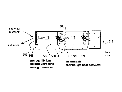
thermal gradient converters are connected in series thermally and
electrically. This
interconnection referred to as "series-parallel" does not preclude series
parallel configurations
used to assure reliability. For example, the negative electrode 508 of the
chemically energized
generator is electrically and thermally coupled to the positive electrode of
low charge carrier
effective mass region 501 of the nanoscopic thermal gradient converter. The
negative electrode
503 and the high carrier effective mass material 502 of the thermal gradient
converter are
14
CA 02674337 2009-07-02
WO 2008/085757 PCT/US2007/088972
coupled thermally to the colder, heat sink 510. Electricity is taken from the
positive electrode
of 506 and the negative electrode 503, and because the devices are in series
for this example,
also from positive electrode of 501 and negative electrode 503. Note the
output voltage may be
tapped from any of the positive and negative electrode pairs. Note that such
multiple outputs
are highly advantageous.
[0051] This configuration permits the chemically energized generator to
operate at a higher
catalyst temperature than without the nanoscopic thermal gradient converter,
permitting an
increase in reaction rates and therefore higher power density. The increased
temperature also
permits use of a wider range of reactants and operation at the ignition
temperature of some
reactants.
Recursive Nanoscopic Thermal Gradient Converters
[0052] Referring to Figure 6, one embodiment recursively repeats nanoscopic
thermal gradient
converters, each connected in series to the next both electrically and
thermally. The first stage
601 can be an electric generator energized by any of the many known methods
[0053] The recursively repeated nanoscopic thermal gradient converters 602
then generate
electricity from the higher temperature reject heat of the first stage 601 and
the lower
temperature ambient heat sink. Estimates suggest that a recursively repeated
nanoscopic
thermal gradient converter can achieve ¨ 80% of the Carnot limit efficiency
between its heat
source and heat sink temperatures.
[0054] Note again, an output voltage may be tapped from any of the positive
and negative
electrode pairs.
BALLISTIC REFRACTION ENERGY CONVERTERS
[0055] One generalized embodiment is the surface ballistic refraction energy
converter.
Another is the volumetric ballistic refraction energy converter. Other forms
and combinations
may also be used.
[0056] The term "volumetric" refers to configuration where the active surfaces
and reactant
and coolant flow channels are formed on or using three dimensional structures.
Surface Ballistic Refraction Energy Converter (SBREC)
[0057] One embodiment uses a primary energy converter attached to a series of
secondary
nanoscopic thermal gradient converters attached to a heat sink. Figure 6 shows
such a typical
CA 02674337 2009-07-02
WO 2008/085757 PCT/US2007/088972
surface ballistic refraction energy converter. A number of secondary
nanoscopic thermal
gradient converters 602 are connected in series. One end of the series 602 is
attached to a heat
sink 603. The other end of the series 602 is connected to a primary energy
converter 601 based
on the pre-equilibrium ballistic charge carrier refraction process. The
primary energy converter
may be energized by chemical reactions, thermal gradients, photo-voltaic or
other means. The
number of components 602 may be from 0 to a desired number, both inclusive.
The main
function of the components of 602 is to convert a fraction of the reject heat
energy from the
previously connected energy conversion component to an electrical potential.
[0058] One embodiment includes a primary converter 601, with a step increase
in charge
carrier mass between the junction materials, where the electrons are energized
by chemical
reactions on or near the conducting surface, with 0 to desired number of
nanoscopic thermal
gradient converters 602 connected in series electrically and thermally and
attached to a heat
sink.
[0059] One embodiment includes a primary converter 601, without a step
increase in charge
carrier mass between the junction materials, where the electrons are energized
by chemical
reactions on or near the conducting surface, with one to a desired number of
nanoscopic
thermal gradient converters 602 connected in series electrically and thermally
and attached to a
heat sink.
[0060] One embodiment includes a primary converter 601, using a photo-voltaic
energy source
with or without the step increase in charge carrier mass between the junction
materials, and
with one to a desired number of nanoscopic thermal gradient converters 602
connected in series
electrically and thermally and attached to a heat sink.
[0061] One embodiment includes a primary converter 601, a thermionic energy
converter
where charge carrier ballistic transport occurs in the first material instead
of the second
material, with zero to a desired number of nanoscopic thermal gradient
converters 602
connected in series electrically and thermally and attached to a heat sink.
[0062] One embodiment includes a primary converter 601, a thermionic energy
converter with
a second material effective charge carrier mass greater than the first
material charge carrier
mass, with 0 to desired number of nanoscopic thermal gradient converters 602
connected in
series electrically and thermally and attached to a heat sink.
[0063] One embodiment includes a primary converter 601, a thermionic energy
converter with
a second material effective charge carrier mass greater than the first
material charge carrier
mass and where charge carrier ballistic transport occurs in the first material
instead of the
16
CA 02674337 2015-11-25
75873-7
second material, with 0 to desired number of nanoscopic thermal gradient
converters 602
connected in series electrically and thermally and attached to a heat sink.
[0064] One embodiment includes a primary converter 601, attached to a series
of nanoscopic
thermal gradient converters 602, one or more of which may include a dielectric-
conductor-
dielectric junction for the region generally referred to as the low carrier
effective mass region,
and connected in series electrically and thermally and attached to a heat
sink. The number of
nanoscopic thermal gradient converters may be from 0 to the number desired,
both inclusive.
Volumetric Ballistic Refraction Energy Converter (VBREC)
[0065] One embodiment includes volumetric ballistic refraction energy
converters on a pillar-
like form. A desirable feature of the pillar is a high area per length, which
results in a high
volume power density resulting from the pillar's relatively large area per
volume. The cross
section of such a high area pillar may include deep corrugations, holes and
pits, all of which
may be irregular. The cross section of a pillar is limited mainly by the
constraints imposed by
the converters formed on it and has no general constraints. For example, the
cross section may
be any combination from the group including at least: wire-like, circular, bar-
like, square,
rectangular, irregular, wrinkled, sponge-like, a truncated cone, a tapered
cone, and a cross
section like that of wings or other aerodynamic forms.
[0066] Referring to Figure 7, the pillar itself 701 can be can be any
material, such as strands,
fibers, strips formed with one or more materials each chosen for their
strength, thermal
conductivity, electrical conductivity, or any other desirable property.
[0067] A pillar would first be at least partly coated with a conductor 702 to
form the back
electrode of the device. Then as many as required secondary nanoscopic thermal
gradient
converters 703 are formed over the pillar and under a final primary energy
converter 704, with
or without a step increase in charge carrier mass between the junction
materials. The primary
energy converter 704 may be energized either chemically, photo-voltaically, by
thermal
gradients or other means. The outer region 705 is the source energizing
region. The number of
units 703 range from zero to the required number, both inclusive. The positive
electrode
connection 706 is in electrical contact with the final converter 704. An
insulator 707 separates
the positive electrode connection 706 from the negative electrode connection
708, which is in
electrical contact with the conductor 702. Heat sink can be provided by the
reactants and gasses
surrounding the pillar region 705 and or by the substrate 709 which can be
physically
connected to a heat sink.
17
CA 02674337 2015-11-25
75873-7
[0068] One embodiment includes a primary converter 704 where the electrons are
energized by
chemical reactions on or near the conducting surface, with 0 to a desired
number of nanoscopic
thermal gradient converters connected in series electrically and thermally and
attached to a heat
sink.
[0069] One embodiment includes a primary converter 704, a photo-voltaic energy
converter
with 0 to a desired number of nanoscopic thermal gradient converters connected
in series
electrically and thermally and attached to a heat sink.
[0070] One embodiment includes a primary converter 704, a thermionic energy
converter with
0 to a desired number of nanoscopic thermal gradient converters connected in
series electrically
and thermally and attached to a heat sink.
[0071] One embodiment includes long mean free path semiconductors as well as
long mean
free path metals as the materials forming the minimum charge carrier effective
mass region.
Band gap alignments may be used to form potential barriers.
[0072] One embodiment includes a primary converter 704, a solid state thermal
gradient energy
converter using a dielectric-conductor-dielectric junction attached to a
series of similar
nanoscopic thermal gradient converters connected in series electrically and
thermally and
attached to a heat sink. The number of nanoscopic thermal gradient converters
may be from 0
to the number desired, both inclusive.
[0073] In general, ballistic refraction energy converters can be attached to
various kinds of
objects, including to devices used to cause reactant flow, air flow, and
cooling, such as such fan
blades. It can take the form of a sheet following the contour of the objects.
For example, the
converters can be "coated" on to the air flow system. Alternatively, the
converters can be
separately made and "pasted" on to the system. Or, they can be integral to the
system.
[0074] In some embodiments, placing ballistic refraction energy converters
directly on the fan blade
may maximize the efficiency with which the fan provides cooling, heat transfer
and heat removal.
[0075] As suggested by Figure 8, ballistic refraction energy converters 801
affixed to the pillar
with cross section profile 802 may be any shape consistent with the
requirements for making
the ballistic refraction energy converters. A large energy collection area is
desirable and may
be achieved in many ways, including forming the profile to include long, thin
forms 802,
wedges 803, channels 804, irregular polygonal sides 805, deep narrow channels
or pores 806,
pores that completely go through the pillar 807, symmetric forms 808 and 803,
almost
symmetric forms 809, and smoothly symmetric forms 810.
[0076] Pores can take the form of deep holes into the stack 804, or as holes
that go entirely
through the stack 807.
18
CA 02674337 2009-07-02
WO 2008/085757 PCT/US2007/088972
Wire Geometry
[0077] One embodiment forms a converter geometry resembling a long thin device
such as a
wire 802. The converter wire can be preformed and poked into the surface or
otherwise
attached to the surface in regular or irregular patterns.
Flow Geometry
[0078] One embodiment provides a heat sink for ballistic refraction energy
converters. A heat
sink for cooling can be achieved in many ways, including by convective flow,
phase change or
evaporative cooling, and heat pipes. Reactants or reactant components may be
used. For
example, Figure 9 illustrates an embodiment using channels, ducts or pipes
associated with the
structure supporting the converters and with the interior of the converter
assembly, through
which coolant may flow, reactants may flow, additives may flow, or any
combination of these
materials may flow. Each case has its advantages. Materials 901 flow from the
colder side 902,
through pores or holes 903 to the hot region 904. Both the cold side 902 and
the hot side 904
may include reactants or additives, and the hot side is associated with both
exhausts and air
flow.
[0079] Evaporation of reactants 901 on the cold side 902 as well as the flow
of colder materials
901 causes cooling. Reactants 901 can be concentrated and fuel rich near the
stack hot surface
905.
[0080] Using liquid reactants or evaporative coolant 901 that becomes gas upon
contact with
warmer, reaction surface 905 provides a desirable gas specie for chemically
energized hot
electron processes.
[0081] One embodiment forms converters directly on aerodynamic surfaces. This
permits both
direct generation of electricity as well as using the gas generated by the
liquid-gas
transformation as mass flow to push a turbine or other mechanical extraction
of useful work
and generation of shaft energy.
[0082] One embodiment uses liquid air and other liquid gasses 901 for their
low temperature
heat sink in an electric generator. Liquid air and similar inert liquid gasses
may provide a heat
sink to the region 902, the ambient air in the exhaust region 904 may provide
the heat source,
and the device may thereby generate electricity directly using the temperature
difference. The
liquid / gas phase transition may also operate a mechanical energy converter
such as a turbine,
at the same time.
19
=
CA 02674337 2015-11-25
75873-7
[008.3] One embodiment uses natural convection to provide air flow. It is
noted that the cooling
air volume can typically be orders of magnitude greater than the reaction air
volume.
[0084] One embodiment based on Figure 9 may also represent the cross section
of generalized
tube geometry, such as flattened tubes. A generalized tube is coated on one or
more faces with
ballistic refraction energy converters. "Tube" here refers to something with
any partly hollow
geometry, with any relative wall thickness, including non-uniform walls. For
example, a tube
can be flattened so that it looks like two sheets with an enclosed space
between them to allow
gas or fluid flow and with the volume enclosed at the edges. Note that the
concepts of Figure
9 could be used in surface as well as volumetric devices (SBREC and VBREC).
Stacking Geometry
[0085] Referring to Figure 10, an elementary stackable unit is placed on a
structure that
includes one or more of the electrically conducting layer, thermally
conducting layer, and the
structural support layer.
[0086] Some embodiments connect and stack together more than one ballistic
refraction
energy converter (surface (SBREC), or volumetric (VBREC)) assembly to create a
volume of
= electric generators instead ofjust an area provided by the surface of a
single converter
assembly. The stacks can be connected electrically in series or parallel.
= [0087] One embodiment of an elementary stackable unit, shown in cross
section in Figure 10,
includes the key element: ballistic refraction energy converter assembly 1001
(which may
comprise of primary only or primary and secondary energy converters) to be
connected
electrically with positive and energized side 1004 up and negative side down.
The ballistic
refraction energy converters are supported and connected with positive
electrode connection
1002, negative electrode connection 1003. Structure 1003, which may include
one or more of
an electrically conducting element, a thermally conducting element and a
strength structure
element. Stacking involves placing the elementary stackable unit on top of
other elementary
stackable units, leaving a space above the active surface of the converter
1001 for energizing
and heat sources. The same may be accomplished in any workable configuration
or
arrangement.
[0088] The embodiment shown in Figure 10 connects the positive electrode 1002
to the
negative electrode 1003 of the converter above it. A cross section of this is
shown in Figure 11.
Note that each elemental structure of Figure 11 may be recursively stacked in
the vertical
and/or in the horizontal direction to form a matrix of the three-dimensional
elemental stacked
structures.
CA 02674337 2009-07-02
WO 2008/085757 PCT/US2007/088972
[0089] Figure 10-b provides detail related to electrical and thermal
connections and interfaces
that have been deliberately left out for clarity in the embodiments.
[0090] Referring to Figure 10-b, for example, the positive electrode-1002
would not be directly
placed on the active surface of the converter 1001 as shown because the active
surface is
typically a nanometers-thick structure that is easily damaged. In practice,
those generally
skilled in the art would use one of many known methods to connect the
electrode to the
converter. One embodiment places the positive electrode 1002 on an insulator
1005 formed
directly on the structure 1003 and then an electrical bridge 1006 is formed to
electrically
connect the positive electrode 1002 to the positive end and active surface
1004 of the ballistic
refraction converter assembly. The structure element 1003 would in practice
include an
electrical conductor connected to the negative side of the converter and would
also include a
thermal connection to the converter. A simple embodiment forms the structure
1003 to be both
electrically and thermally conducting, for example a 5 micron thick aluminum
or copper foil.
[0091] One embodiment stacks the elementary stackable units shown in Figure 10
on top of
each other, forming a volume of electric generator energy converters.
Reactants and coolants
1100 flow into the spaces 1101 between the stacks and exhausts flow out
through the spaces.
[0092] One embodiment connects the converters in series along the plane of the
stack by
connecting the positive electrode to the negative electrode of adjacent
converters in the same
plane. This can be accomplished several ways, one of which is shown in Figure
12. An
electrical connection 1202 is made to the positive side and active surface of
a first converter
1201 and is connected to an interconnecting conductor 1203 isolated by
insulators 1204. The
interconnect 1203 electrically contacts the negative side 1205 of a second
converter. The
insulating spacer 1200 is shown conceptually behind a converter in the figure.
[0093] One embodiment provides coolants and/or reactants 1300 through the body
of an
elementary stackable unit, as sketched in Figure 13. For example, ballistic
refraction energy
converters 1301 and spacers 1302 are formed on a structure and substrate 1303
inside of which
1304 flow reactants and/ or coolants 1300. Referring to Figure 18, the device
of this
embodiment can be rolled up and the spaces 1305 between the roll formed by
spacers 1302
permit reactants to flow into and exhausts can flow out of the spaces 1305.
The spacers and
electrical interconnects are shown in Figure 13 for clarity. Detailed
connections could also be
like those explained in Figure 12 and Figure 10-b.
[0094] In each of these embodiments, the converters can take on many forms,
including the
pillar forms described above, and can be attached on many surfaces of nearly
arbitrary shapes.
21
CA 02674337 2009-07-02
WO 2008/085757 PCT/US2007/088972
Tunneling Cluster Catalysts
[0095] One embodiment uses physically disconnected, electrically tunneling
connected
nanoscopic catalyst clusters to enhance the effective temperature gradient of
excitations on the
active surface of a ballistic refraction energy converter. Figure 14
schematically shows
conductor catalyst structures 1400 with typical dimension D and typical
separation S on the
converter 1401 with active surface 1402. The dimension D is formed to be less
than the mean
free path for hot carriers in the cluster 1400, chosen to allow the carrier
transit time to be
shorter than the period of the highest lattice vibration of the cluster 1400
and hence decouples
carrier temperature from lattice temperature. This dimension is typically in
the range of order 4
to 50 nm in materials such as Cu, Ag, Au, Pd, and Pd. The cluster separation D
is chosen to be
small enough to permit charge carrier electron tunneling between clusters
1400. This dimension
is typically in the range 1 - 20 nm. Electrical connections to the cluster are
formed by electrical
conductor contacts 1403 and 1404. In an ideal case, the disconnected clusters
are formed on a
low electrical conductivity and low thermal conductivity material. This
cluster arrangement
can then form a Schottky barrier with the converter 1401, permitting the
clusters to be an
integral part of a ballistic refraction energy converter.
[0096] One embodiment uses the enhanced catalyst activity of catalyst clusters
in contact with
ceramic substrates such as converter material. One embodiment uses the
enhanced cluster
electron temperature to increase reaction rates and therefore increased power
output. One
embodiment applies an electrical potential across electrodes 1403 - 1404,
which has been
shown to heat the clusters to temperatures (-2000 K - 5000 K) far in excess
the substrate
temperature ( ¨ 300 K) and hence can greatly increase reaction power without
increasing
converter diode temperature.
Coupling and Conversion Layers
[0097] One embodiment uses a quantum well superlattice for the lowest charge
carrier
effective mass material. To maximize conversion efficiency, the superlattice
is tailored such
that it filters carriers with energies slightly greater than the barrier
height from the low carrier
effective mass region to the high carrier effective mass region.
[0098] One embodiment forms closely spaced buss bars on the active surface to
minimize
ohmic losses across the surface. Chemically inactive buss bars are formed as
close as 100 nm
apart, with active material such as tunneling cluster catalysts between the
buss bars.
22
CA 02674337 2009-07-02
WO 2008/085757 PCT/US2007/088972
[0099] One embodiment uses very thin semiconductor for the barrier-presenting
material. The
minimum thickness is typically of order 5 nm. A preferable semiconductor
thickness is in the
range between 20 and 100 nm although other thicknesses are contemplated.
Thermal Conductivity Management
[00100] Referring to Figure 15, one embodiment tailors the lower charge
carrier
effective mass region 1500-1501 to include elements for controlling and
limiting the transfer of
heat, and enhancing the transfer of charge carrier kinetic energy. These
elements include one or
more of low thermal conductivity materials, long carrier mean free path
materials, thermal
diode elements, quantum confinement elements and graded carrier effective mass
elements.
The principle is to present multiple regions of increasing carrier effective
mass to the charge
carrier as it travels ballistically towards the barrier region. Figure 15 show
two such regions
1500, 1501.
[00101] Referring to Figure 15, one embodiment uses a semiconductor (S)
1500 with a
charge carrier effective mass as low as practical, such as silicon with a
charge carrier effective
mass ¨ 0.3 m_e in contact with a conductor (C) 1501 with a higher charge
carrier effective
mass and known to have unusually long electron mean free paths at ¨ 1 eV. Such
conductors
1501 include, for example, Au (-20 - 100 nm), Ag (¨ 20 nm) and Cu (reported as
high as 60
nm) and Al (-20 nm). A ballistic charge carrier refraction effect then exists
between the
semiconductor 1500 and the conductor 1501. The semiconductor 1500 may then
inject its
hotter charge carriers via a narrow range of directions into the conductor C
1501. The
conductor C 1501 is chosen to have a thickness less than approximately 2 times
a charge carrier
mean free path. Nearly all charge carriers traveling through the conductor C
1501 are already
directed towards the semiconductor S_barrier 1502, for example TiO2 with
charge carrier
effective mass ¨25 m_e, higher than 1501 charge carrier effective mass.
[00102] Materials with electron effective mass less than 1.1 and
materials with
relatively long electron mean free paths can be used for either semiconductor
1500 or lowest
charge carrier effective mass material 1500, including, but not limited to:
air, aluminum,
conducting carbon nanotubes, conductors, copper, degeneratively doped
materials, gasseous
material, gold, metals, metals, molybdenum, nickel, palladium, platinum,
rhodium, ruthenium,
silver, tantalum, vacuum. The materials with a ZT figure of merit greater than
approximately
0.05 and generally preferred for thermoelectric applications may also be used
for lowest charge
carrier effective mass material 1500, including but not limited to: aluminum
antimonide
(AlSb), aluminum arsenide (AlAs), aluminum gallium nitride (AlxGal-xN),
bismuth selenide
(Bi2Se3), bismuth telluride (Bi2Te3), and boron nitride (BN), gallium aluminum
arsenide
23
CA 02674337 2009-07-02
WO 2008/085757
PCT/US2007/088972
(GaxAl 1 xAs), gallium aluminum arsenide antimonide (GaxAll xAs1 y), gallium
antimonide
(GaSb), gallium arsenide phosphide (GaAsyP1 y), gallium arsenide, gallium
indium
antimonide (GaxInl-xSb), gallium indium phosphide (GaxInl xP), gallium nitride
(GaN),
gallium phosphide (GaP), germanium (Ge), indium aluminum arsenide (InxAll
xAs), indium
antimonide (InSb), indium arsenide (InAs), indium arsenide phosphide (InAsyP1-
y), indium
gallium aluminum arsenide (InxGyAll x yAs), indium gallium arsenide (InxGal-
xAs),
indium gallium arsenide antimonide (InxGal xAsySB1 y) indium gallium arsenide
phosphide
(InxGa 1 xAsyP1 y), indium gallium nitride (InxGal-xN), indium phosphide, lead
telluride,
lead tin telluride (Pbx Snl xTe), mercury cadmium selenide (HgxCd.1 xSe),
mercury
cadmium telluride (HgxCd1-xTe), silicon germanium, silicon, zinc selenide
(ZnSe), zinc
telluride (ZnTe), where the subscripts x, y, z, 1-x,and 1-y denote the
relative amounts of the
atomic species in each ternary or quartenary materials and range from zero to
one, inclusive.
[00103] The
barrier-presenting layer 1502 may be made from materials including but
not limited to semiconductors known to have carrier effective masses greater
than 2, including
but not limited to: ruffle TiO2, anatase TiO2, porous anatase TiO2, SrTiO3,
BaTiO3, Sr_x-
Ba_y-TiO_z, LiNiO, LaSrV03, organic semiconductors PTCDA, (3,4,9,10-
perylenetetracarboxylicacid-dianhydride). The following materials and
semiconductors with at
least favorable ZT figure of merits and generally preferred for thermoelectric
applications may
also be used when their charge carrier effective masses are greater than two
times that of the
material chosen for their junction, including but not limited to: aluminum
antimonide,
aluminum gallium arsenide, aluminum oxide, bismuth selenide, bismuth
telluride, boron
nitride, gallium aluminum arsenide antimonide, indium aluminum arsenide
phosphide,
indium gallium alluminum nitride, indium gallium arsenide antimonide, indium
gallium
arsenide phosphide, lead europium telluride, lead telluride, and air. lead tin
telluride, mercury
cadmium selenide, mercury cadmium telluride, silicon germanium, silicon oxide,
zinc
selenide, zinc telluride.
[00104] The conductor becomes more like an insulator against heat energy
transport, on
the timescale of ballistic transport, and a very good, one directional
conductor for charge carrier
energy transport in the present thermoelectric and thermionic energy
converters. Within this
nanoscopic dimension the conductor can sustain a useful temperature gradient
across it. The
thermal isolation of the nanoscopic sandwich 1500-1501-1502 increases the
efficiency of the
electric generator process.
[00105] The addition of a low charge carrier effective mass material, a
conductor 1501,
between a lower charge carrier effective mass material 1500 (with values as
low as 0.02 me),
24
CA 02674337 2009-07-02
WO 2008/085757 PCT/US2007/088972
and a highest charge carrier effective mass material 1502 (with values as high
as 200, m_e,
such as Ti02), expands the range of materials that may be used in a solid
state energy converter.
[00106] One embodiment includes catalyst clumps 505 physically isolated
and
electrically connected through electron tunneling. The clumps 505 replace at
least some and in
some configurations the entire conductor 506 on the surface of an electric
potential barrier
(dielectric) material 507.
[00107] Another embodiment uses such nanoscopic constraints on the
dimension of
conducting catalyst clusters, sheets, nano-wires, nano-dots, nano-tubes,
quantum dots, layers
and constructs 505 to enhance reaction rates in chemically energized pre-
equilibrium energy
converters.
Tailoring Charge Carrier Thermal Coupling
[00108] According to one embodiment the energy transfer between materials
in contact
with the heat or hotter electron source and the colder region are controlled
to be predominantly
by ballistic charge carrier transport. Referring to Figures 16-A through 16-D,
we show a cross
section of a device using three materials or regions. As a general governing
principle, the first
and second regions, 1601 and 1602, are designed to block heat and transmit
energized, ballistic
carriers with minimal energy loss. The ideal condition is the transport of
energy only by
ballistic electrons (charge carriers) and not by heat, from region 1601, 1602
to region 1603. As
a general governing principle, third region 1603 is designed to pass only the
more energetic
ballistic charge carriers against and over an electrical potential barrier,
and to refract the
direction of the ballistic carriers so they transport directly into the
potential. The refraction is
enhanced when the third region 1603 has a carrier effective mass at least two
times higher that
of the conductor region 1602, and is overwhelmingly so when it is higher by at
least a factor of
2. The first and second regions 1601, 1602 are generally characterized by a
favorable ZT
thermoelectric figure of merit. The second region 1602 is generally
characterized by an
enhanced tendency to transmit a large number of ballistic electrons, and this
is generally
referred to as having a relatively long mean free path.
[00109] The first material 1601 may have a higher, equal or lower charge
carrier
effective mass than the second material 1602. In addition, the first material
1601 may or may
not present an electrical potential barrier to carriers traveling, backwards
from the second
material 1602 back into the first material 1601. These two options result in
four cases, each
case having relative advantages. The choice depends on material availability,
manufacturability, cost, stability and other factors.
CA 02674337 2009-07-02
WO 2008/085757 PCT/US2007/088972
[00110] One embodiment including the first case Figure 16-A, with minimal
or no
barrier in the first material and an increasing charge carrier effective mass
from left to right
1601, 1602, 1603, offers the fastest and shortest path transfer of energetic
electron energy into
the barrier material with highest charge carrier effective mass 1603. Nearly
any of the common
semiconductors may be used as the first material because virtually all of them
are commercially
valuable precisely in part because their charge carrier effective masses are
all low, less than 1
m_e. This means that all the known favorable ZT materials can be used very
effectively. A
minimal barrier can be achieved by band gap engineering or degenerative
doping.
[00111] One embodiment including the second case Figure 16-B, with minimal
or no
barrier in the first material 1601 and since the middle material 1602 has the
lowest charge
carrier effective mass, it allows charge carriers in the middle material to
exit the material more
easily than allowing entry of charge carriers from materials 1601 and 1603.
For example,
electrons that have energies too low to surmount the barrier in material 1603
are not only
reflected back into middle material 1602 but also are quickly transported to
the warmer
material 1601 for reheating and reprocessing. The middle, inner region 1602 is
electronically,
and therefore in the case of ballistic transport, thermally isolated to the
outer regions 1601,
1603. This tends to minimize energy transfer from electrons to lattice, which
in turn minimizes
heat conductivity losses. The back-to-back ballistic refraction tends to
isolate the two heat bath
regions 1601 and 1603.
[00112] One embodiment including the third case Figure 16-C, with a
barrier in the first
material 1601 and an increasing charge carrier effective mass, provides
fastest transport of
only the hottest charge carrier of the first material 1601.
[00113] One embodiment including the fourth case Figure 16-D, presents
electrical
barriers against charge carrier transport back into the hotter material 1601
and into the colder
material 1603, and has the minimum charge carrier effective mass in the middle
material 1602.
This configuration almost reversibly communicates carrier energy between two
heat baths,
which is a key property, and because of the ballistic transport, and
preferentially transports
charge carrier energy faster than by lattice phonon or other energy transfer.
Note that ballistic
transport is only necessary in the middle region 1602 and not in the
surrounding regions 1601,
1603. The charge carrier may be negative or positive, and the barriers are
designed to retard
transport. Example materials for the regions can be, for example, TiO2 for the
outer regions
and Silicon for the middle region, where band gap alignments provide the
barrier. The middle
region 1602 materials can be chosen from the group including at least metals
with long mean
free paths, such as Cu, Au, Ag, Al, and materials with high ZT.
26
CA 02674337 2015-11-25
75873-7
[00114] One embodiment uses the same barrier region material on both
sides of the
conductor.
[00115] One embodiment to use thermally energized ballistic refraction
energy
converters as refrigerators utilizes one or more stacked converters and
applies a positive
potential across the terminals instead of the negative potential obtained from
the same device
used as a generator. The heat sink may then be hotter than the heat source,
and cooling occurs
because the hot electrons are efficiently removed from the cooled regions. The
use of ballistic
refraction enhances the efficiency of such a cooling method and device over
devices where
carriers are not directed predominantly into the potentials at the interfaces
of low and high
charge carrier effective mass materials.
[00116] Some embodiments form one or more refrigerating ballistic
refraction energy
converters directly on integrated circuits to cool them. A similar embodiment
forms a
refrigerating ballistic refraction energy converter directly on chemical
reaction surfaces, for
example, to control reaction pathways and control reactions.
=
Fuels, Oxidizers, Autocatalysts, Stimulators
[00117] Embodiments use storable reactants including oxidizers,
autocatalytic reaction
accelerators, decelerators, and monopropellants. The liquid phase, such as
liquid hydrogen
peroxide H202 at standard pressure and temperature, are convenient because
their heat of
vaporization is used as coolant and the liquid is conveniently storable.
Monopropellants such as
H202 and monomethylhydrazine (MMH) are similarly convenient and energize the
active=
surface of converters. Autocatalytic accelerators include monopropellants such
as H202.
[00118] One embodiment uses thermally isolated catalysts in close
proximity to the
active surface of ballistic refraction converter assemblies to enhance
reaction rates and
concentrate thermally hot entities to the thermally hot region of the
converter.
[00119] Figure 17 shows'an embodiment where a highly reactive catalyst
1701 is placed
on a thermally isolated pillar structure 1702 in close proximity to the active
surface 1703 of a
converter. Gas phase reaction products created in the vicinity of the catalyst
energize the
converter. The products may include one or more of at least highly
vibrationally excited
molecules, reactive molecules, and hot gases.
[00120] Some embodiments use energetic reactants chosen to maximize the
energizing of
highly energetic specie, which include one or more of highly vibrationally
excited molecules
(HVEM), hot atoms, charged adsorbate intermediates such as peroxo and superoxo
specie
formed during precursor mediated dissociative adsorbsion, adsorbates
participating in
27
CA 02674337 2015-11-25
=
75873-7
association reactions both of the Langmuir-Hinshelwood and of the Eley-Rideal
type, and
reaction intermediates such as radicals, free radicals and specie considered
to be catalytic or
autocatalytic.
[00121] Some embodiments provide means for the energizing to occur
directly on or in
the vicinity of a conductor. The term "vicinity" refers here to a distance
less than a few mean
free paths of the particular energetic excitation. Some embodiments use these
excitations to
energize a low charge carrier effective mass material of the ballistic
refraction energy converter.
[00122] Chemical reactions using reactants of this kind result in pre-
equilibrium
excitation including reaction effective temperatures and effective carrier
temperatures in excess
of 10,000 Kelvin on and in metals, conductors, catalysts, semiconductors and
ceramics, and
where the carriers include excitons, carriers in the conduction and/or valence
band of
semiconductors and insulators.
[00123] One embodiment uses reactions and reactants to energize these
excitations. The
reactions, reactants and additives include at least monopropellants, high
energy fuels with
oxidizers, hypergolic mixtures, and additives and combinations of reactants
known to produce
autocatalytic specie, reactants chosen to accelerate reactions or to control
reactions, and
combinations thereof. The reactants and/or additives include but are not
limited to the
following reactants:
Table I
energetic fuels more storable than ammonia
amine substituted ammonias
Di-Methyl-Amine (CH3)2NH
Tr-Methyl-Amine (CH3)3N
Mono-Ethyl-Amine (C2H5)NH2
Di-Ethyl-Amine (C2H5)2NH)
other classes more easily storable
Methanol, CH3OH
Ethanol, Et0H CH3CH2OH
Formic Acid, HCOOH
diesel fuels
gasoline
alchohols
28
CA 02674337 2009-07-02
WO 2008/085757
PCT/US2007/088972
slurries including solid fuels
Carbon Suboxide, C302 , CO=C=CO,
Formaldehyde HCHO,
Paraformaldehyde, = better HCH0),, , sublimeable to Formaldehyde gas.
(Potentially a cell coolant at the same time).
less storable fuels
Carbon Monoxide
Hydrogen
Ammonia NH3
energetic fuels containing Nitrogen
Nitromethane, CH3NO2
Nitromethane "cut" with Methanol = model airplane "glow plug" engine fuel
High energy fuels with wide fuel / air ratio
Epoxy-Ethane, = Oxirane or Ethylene-Oxide CH2-CH2 0
1,3-Epoxy-Propane = Oxetane and Tri-Methylene-Oxide = 1,3-Methylene-Oxide
CH2-(CH2)-CH2 0
Epoxy-Propane CH2-(CH2)-CH2 0
Acetylene, C2H2
Diacetylene = 1,3-Butadiyne
1,3- Butadiene CH2=CH-CH=CH2,
less exotic high energy fuels
Di-Ethyl-Ether or surgical ether
Acetone = Di-Methyl-Ketone
less exotic, volatile fuels
Cyclo-Propane
29
CA 02674337 2009-07-02
WO 2008/085757 PCT/US2007/088972
Cyclo-Butane
Hydrocarbons such as methane, propane, butane, pentane, etc.
other storable fuels
Methyl Formate HCOO-C2H5
Formamide HCO-NH2
N, N, -Di-Methyl-Formamide HCO-N-(CH3)2
Ethylene-Diamine H2N-CH2-CH2-NH2
Ethylene-Glycol
1,4-Dioxane =bimolecular cyclic ether of Ethylene-Glycol
Paraldehyde (CH3CH0)3 cyclic trimer of Acetaldehyde
powerful oxidizer
Tetra-Nitro-Methane, C(NO2)4 ... does not spontaneously decompose ... just
pass
the two separate vapors over the reaction surface of the cell in the gas phase
Hydrogen Peroxide H202
low initiation energy mixtures
Cyclo-Propane with Oxygen = surgical anesthetic, microjoules initiator
Hypergolics
UDMH = Unsymmetrical DiMethyl Hydrazine = 1,1-DiMethyl Hydrazine
(CH3)2NNH2
UDMH is hypergolic usually with N204 and is a very potent carcinogen
MMH MonoMethyl Hydrazine (CH3)HNNH2 hypergolic with any oxidizers, e.g.
N204
Corrosive Toxic energetic monopropellant
Hydrazine = H2NNH2 decomposed easily with a catalyst (usually Pt or Pd or
Molybdenum Oxide
Hydrazine Hydrate
CA 02674337 2009-07-02
WO 2008/085757 PCT/US2007/088972
[00124] A method and system for ballistic charge carrier refraction have
been disclosed.
Although the present methods and systems have been described with respect to
specific
examples and subsystems, it will be apparent to those of ordinary skill in the
art that it is not
limited to these specific examples or subsystems but extends to other
embodiments as well.
31