Note : Les descriptions sont présentées dans la langue officielle dans laquelle elles ont été soumises.
CA 02676495 2009-08-24
MECHANICAL BARRIER ELEMENT FOR IMPROVED THERMAL RELIABILITY OF
ELECTRONIC COMPONENTS
BACKGROUND OF THE INVENTION
Field of the Invention
[0001] The present invention is generally related to packaging of integrated
circuit
devices, and more specifically providing a thermal paste for cooling an
integrated circuit
device during operation.
Description of the Related Art
[0002 Since the invention of the transistor, dissipation of heat during
operation has
been an important consideration in semiconductor device package design. Heat
can
damage the delicate and tiny structures which allow transistors to function as
intended
in a semiconductor device. Power drawn by transistors and other electronic
devices
must be dissipated to avoid build up of heat and the development of high
temperatures
which can degrade the devices by such mechanisms as dopant diffusion, metal
migration including solder softening and reflow, or the like.
[0003) As semiconductor devices become smaller and smaller, it has become more
difficult to provide efficient heat dissipation mechanisms. Current designs
provide
thermal pastes in conjunction with heat sinks that facilitate internal cooling
of the
semiconductor devices. Thermal pastes are generally high thermal conductivity
interface materials that fill the gaps between the back-side of integrated
circuit chips
and the inside surfaces of heat sinks. Generally, semiconductor device package
components, like the back surface of the integrated circuit and the inside of
the cap
must be chemically compatible with the thermal paste, so that the paste can
adhere to
them. Furthermore, the package must be designed such that the thermal paste
filled
chip-to-heat sink gap has sufficient thickness that it will form a reliable
and efficient heat
dissipating structure.
CA920090006 1
CA 02676495 2009-08-24
SUMMARY OF THE INVENTION
[0004 The present invention is generally related to packaging of integrated
circuit
devices, and more specifically to the placement of thermal paste for cooling
an
integrated circuit device during operation.
[00051 One embodiment of the invention provides an integrated circuit package,
generally comprising a substrate, an integrated circuit chip coupled with the
substrate,
and a cap configured as a heat dissipation element, wherein a thermal paste
forms an
interface between a top surface of the integrated circuit chip and a bottom
surface of the
cap. The integrated circuit package further comprises at least one barrier
element
formed proximate to at least one side of the integrated circuit chip, wherein
a region
between the barrier element and the at least one side of the integrated
circuit chip
defines a reservoir for excess thermal paste pumped from between the top
surface of
the integrated circuit chip and the bottom surface of the cap.
[0006 Another embodiment of the invention provides a method for fabricating an
integrated circuit package. The method generally comprises providing an
integrated
circuit chip coupled with a substrate, placing a barrier element on the
substrate
proximate to at least one side of the substrate, depositing a thermal paste on
a portion
of a top surface of the integrated circuit chip, and pushing the thermal paste
towards
the integrated circuit chip with a surface of a cap, wherein the pushing
spreads the
thermal paste over the top surface of the integrated circuit chip and into a
region
between the barrier element and the at least one side of the substrate to form
a
reservoir of thermal paste.
[00071 Yet another embodiment of the invention provides an integrated circuit
package, generally comprising a plurality of integrated circuit chips coupled
with a
substrate, a cap configured as a heat dissipation element, wherein a thermal
paste
forms an interface between top surfaces of the integrated circuit chips and a
bottom
surface of the cap, and at least one barrier element formed proximate to at
least one
side of at least one of the integrated circuit chips, wherein a region between
the barrier
element and the at least one side of the integrated circuit chip defines a
reservoir for
CA920090006 2
CA 02676495 2009-08-24
excess thermal paste pumped from between the top surface of the integrated
circuit
chip and the bottom surface of the cap.
BRIEF DESCRIPTION OF THE DRAWINGS
[0008] So that the manner in which the above recited features, advantages and
objects of the present invention are attained and can be understood in detail,
a more
particular description of the invention, briefly summarized above, may be had
by
reference to the embodiments thereof which are illustrated in the appended
drawings.
[0009] It is to be noted, however, that the appended drawings illustrate only
typical
embodiments of this invention and are therefore not to be considered limiting
of its
scope, for the invention may admit to other equally effective embodiments.
[0010] Figure 1 illustrates an exemplary integrated circuit package according
to an
embodiment of the invention.
[0011] Figure 2 illustrates another exemplary integrated circuit package
according to
an embodiment of the invention.
[0012] Figure 3 illustrates yet an exemplary integrated circuit package
according to
an embodiment of the invention.
[0013] Figures 4A-4E illustrate steps for fabricating an integrated circuit
package
according to an embodiment of the invention.
[0014] Figure 5 is a flow diagram of exemplary operations performed during
fabrication of an integrated circuit package according to an embodiment of the
invention.
DETAILED DESCRIPTION OF THE PREFERRED EMBODIMENTS
[0015] Embodiments of the invention are generally related to packaging of
integrated
circuit devices, and more specifically to the placement of thermal paste for
cooling an
integrated circuit device during operation. A barrier element may be placed
along at
CA920090006 3
CA 02676495 2009-08-24
least one side of an integrated circuit chip. The barrier element may contain
thermal
paste pumped out during expansion and contraction of the package components to
areas near the chip. The barrier element may also form a reservoir to
replenish thermal
paste that is lost during thermal pumping of the paste.
[00161 In the following, reference is made to embodiments of the invention.
However, it should be understood that the invention is not limited to specific
described
embodiments. Instead, any combination of the following features and elements,
whether related to different embodiments or not, is contemplated to implement
and
practice the invention. Furthermore, although embodiments of the invention may
achieve advantages over other possible solutions and/or over the prior art,
whether or
not a particular advantage is achieved by a given embodiment is not limiting
of the
invention. Thus, the following aspects, features, embodiments and advantages
are
merely illustrative and are not considered elements or limitations of the
appended
claims except where explicitly recited in a claim(s). Likewise, reference to
"the
invention" shall not be construed as a generalization of any inventive subject
matter
disclosed herein and shall not be considered to be an element or limitation of
the
appended claims except where explicitly recited in a claim(s).
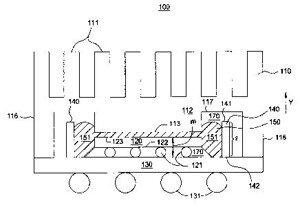
[00171 Figure 1 illustrates a cross-sectional view of an integrated circuit
package 100
according to an embodiment of the invention. As illustrated in Figure 1, the
package
100 includes a cap 110, an integrated circuit chip 120 (hereinafter referred
to simply as
chip), a substrate 130, and at least one barrier element 140. The cap 110 may
be a
heat sink configured to dissipate heat generated by the integrated chip 120.
The cap
110 may include materials that are good conductors of heat. For example, in
some
embodiments, the cap 110 may be formed with copper, aluminum , or like metals.
In
some embodiments, the cap 110 may be made from a metal alloy, for example,
Kovar
(Kovar is a trademark of Carpenter Technology Corporation), CuW, or the like.
In some
embodiments, the cap 110 may be made of a composite material such as, for
example,
Aluminum Oxide, Silicon Cardbide, Aluminum-Silicon Carbide, or the like.
CA920090006 4
CA 02676495 2009-08-24
[0018] As illustrated in Figure 1, in one embodiment, the cap 110 may include
a
plurality of fin or comb like protrusions 111. The protrusions 111 may
increase the
surface area of the cap 110, thereby facilitating fast and efficient
dissipation of heat
received from the chip 120. The cap 110 may receive heat generated by the chip
120
at a protrusion 112 which is generally located over the chip 120 and has a
lower (e.g.,
planar) surface 113 in facing relation with the chip 120.
[0019] In one embodiment of the invention, the cap 110 may be mechanically
coupled with the substrate 130. For example, in Figurel, a leg portion 116 of
the cap
110, may be affixed to the substrate 130 using an adhesive material. Any
reasonable
adhesive material may be used to attach the cap 110 to the substrate 130.
Exemplary
adhesives materials may include, for example, epoxy, solder, silicone
elastomers, or the
like. While the cap 110 is shown attached to the substrate 130 in Figure 1, in
alternative
embodiments, the cap 110 may instead be coupled with the barrier element 140,
or may
simply sit only on top of the chip 120 without being coupled with the
substrate 130. In
other words, the outer leg portions 116 may be omitted in some embodiments of
the
invention.
[0020] While the cap 110 is shown as a single solid structure, in alternative
embodiments, the cap may include a plurality of independent distinct solid
structures
that are coupled together to form the cap 110. For example, in one embodiment,
the
protrusion 112 may be a separate element that is detachable from the rest of
the cap
110. In embodiments where the cap 110 comprises multiple distinct structures,
each of
the multiple distinct structures may be formed with similar or distinct
materials, for
example, the same or different types of metals, plastics, ceramic, or the
like.
[0021] The chip 120 may be any type of integrated circuit including, for
example,
processors, memory controllers, memory devices, or the like. In general, the
chip 120
may include a plurality of transistors, resistors, inductors, capacitors, or
other like circuit
components that consume power and dissipate heat during operation. As
illustrated in
Figure 1, the chip 120 may be electrically coupled with the substrate 130 by
one or
more solder bumps 121. A sealant layer 170 or chip underfill may also be
provided to
CA920090006 5
CA 02676495 2009-08-24
mechanically couple the chip 120 with the substrate 130 and extend the life of
the
solder connections which may be affected by thermal cycling due to CTE
(Coefficient of
Thermal Expansion) mismatch between the chip and substrate materials. In one
embodiment, the sealant layer may also serve to prevent impurities from
reaching the
solder bumps 121 and adversely affecting the transfer of electric signals
between the
chip 120 and the substrate 130. Any reasonable material, for example, an epoxy
resin,
inorganic filler materials, or the like may be used as the sealant 170.
[0022 In one embodiment, the substrate 130 may be a wiring substrate
configured
to route signals from one location of the chip 120 to another location on the
chip 120.
The substrate 130 may also be configured to provide power and/or ground
connections
to the chip 120 via the solder bumps 121. In some embodiments, the substrate
130
may be configured to exchange one or more input and/or output signals with the
chip
120 during operation. While not shown in Figure 1, in some embodiments, the
substrate may include a plurality of chips 120. Accordingly, in such
embodiments, the
substrate 130 may be configured to transfer electric signals from a first chip
120 to a
second chip 120 coupled therewith. Underneath the wiring substrate 130 are
multiple
solder ball connections 131. The solder ball connections 131 may be used to
electrically couple the substrate 130 to another device such as, for example,
a printed
circuit board (PCB) or a chip carrier.
[0023 As illustrated in Figure 1, a thermal paste layer 150 may be provided in
the
gap between the chip 120 and the protrusion 112 of the cap 110. The thermal
paste
layer 150 forms a thermal interface between the chip 120 and the lower surface
113 of
the protrusion 112, allowing heat to be transferred from the chip 120 to the
cap 110. In
one embodiment, the thermal paste 150 may include any combination of silicone
oil,
mineral oil, epoxy oil, aluminum oxide, zinc oxide, boron nitride, aluminum,
or the like.
[0024 The integrated circuit package 100 is commonly known in the industry as
a
flip-chip type package structure. Under this arrangement, most of the heat
generated
by integrated circuit chip 120 is expected to be transferred to the cap 110.
First, the
heat flows from the front side 122 of integrated circuit chip 120 (i.e., a
circuit area) to the
CA920090006 6
CA 02676495 2009-08-24
back side 123 of integrated circuit chip 120. Then, the heat flows from the
back side 123
of integrated circuit chip 120 to the lower surface 113 of cap 110 through
thermal paste
layer 150. Finally, heat flows from the surface 113 of cap 110 to the
protrusions 111 of
cap 110.
[0025] While a flip chip package is described herein, it should be understood
that
embodiments of the invention may be advantageously utilized in other chip
configurations such as, for example, wire bonding configurations. In general,
embodiments of the invention may be used in any type of integrated circuit
package
wherein transfer of heat from an integrated circuit chip to a heat sink is
desired.
[0026 During operation of the chip 120, transistors and other circuit
components of
the integrated circuit may be turned off and on several times. The switching
of
transistors may result in cyclical generation of heat from the integrated
circuit chip 120.
Such thermal cycling may result in the expansion and contraction of the cap
110, the
chip 120, and the substrate 130. The expansion and contraction, particularly
expansion
and contraction along the y axis (see Figure 1), may result in pumping of the
thermal
paste 150, such that the thermal paste 150 moves out of the interface between
the cap
110 and the integrated circuit chip 120.
[0027 The removal of thermal paste from the interface between the cap 110 and
the
chip 120 may be detrimental to the efficient dissipation of heat from the chip
120. For
example, in prior art systems, loss of thermal paste in the interface between
the chip
and the cap may generate voids and/or air pockets at the interface that result
in poor
and uneven thermal conductivity across the interface. Such uneven and poor
heat
dissipation may result in damage to the chip, or to electrical components of
the chip due
to overheating.
[00281 Furthermore, pumped out thermal paste may be deposited at undesired
locations on a substrate, thereby damaging the integrated circuit package. For
example, pumped out thermal paste may interact with adhesive material used to
affix
the cap to the substrate, thereby loosening or even detaching the cap from the
substrate.
CA920090006 7
I
CA 02676495 2009-08-24
[0029] Embodiments of the invention provide at least one barrier element 140
(two
exemplary barrier elements 140 shown in Figure 1) that is configured to
contain the
thermal paste material 150 within desired areas of the package 100. In one
embodiment, the barrier elements 140 may be placed in close proximity to an
edge of
the chip 120. Accordingly, the thermal paste 150 may be contained in a region
that is
close to the chip 120, thereby preventing pumped out thermal paste from
undesirably
interacting with other package components.
[0030] In one embodiment, the barrier element 140 may be formed in a void
region
170 formed between an outer leg 116 of the cap 110, and side wall portions of
the chip
120 and the protrusion 112 of the cap 110, as is illustrated in Figure 1. The
barrier
element 140 may be formed on the substrate 130, thereby allowing the barrier
element
140 to block the flow of thermal paste 150 that is pumped out from a
corresponding side
of the chip 120 from flowing to undesired locations of the package 100.
[0031] As illustrated in Figure 1, in one embodiment, a height I of the
barrier element
140 may be greater than a height m of the chip 120 from a surface of the
substrate 130.
In a particular embodiment, the height I of the barrier element may be between
about
0.1 and 3.0 mm above the height m of the chip 120, and may be between around
0.1 and 5.0 mm away from the chip edge. By providing a barrier element having
a
greater height than the height of the chip 120, the flow of pumped out thermal
material
150 over the top of the barrier element 140 may be avoided.
[0032] The barrier element 140 may be made with any suitable material such as,
for
example, a ceramic, a plastic, metallic, or a composite material. In one
embodiment,
the barrier element 140 may be made sufficiently thin so as not to take up too
much
space in the package 100. For example, in one embodiment, the thickness w of
the
barrier element 140 may be between around 0.025 and 4.0 mm.
[0033] In one embodiment of the invention, the barrier element 140 may be
coupled
with both, the cap 110 and the substrate 130. For example, referring to Figure
1, a top
surface 141 of the barrier element 140 may be coupled with a surface 117 of
the cap
110, and a bottom surface 142 of the barrier element 140 may be coupled with
the
CA920090006 8
CA 02676495 2009-08-24
substrate 130. In such embodiments, the barrier element 140 may be made from a
flexible material capable of bending or otherwise changing its shape to
accommodate
for expansion/contraction of the cap 110 and/or substrate 130 during thermal
cycling.
Alternatively, the cap 130 may include a recess groove configured to receive
an portion
of the barrier element 140.
[0034] In one embodiment of the invention, a region 151 between the barrier
element
140 and a side of the chip 120 may be used to store excess thermal paste that
may act
as a reservoir to replenish pumped out thermal paste from the interface
between the
chip 120 and the cap 110. For example, referring to Figure 1, during expansion
of the
chip 120 and the cap 110 towards each other along the y axis, thermal paste
from the
interface may be pumped out into the reservoir region 151. Subsequently,
during
contraction of the cap 110 and the chip 120 away from each other, thermal
paste from
the reservoir may be sucked into the interface due to the pumping action.
Therefore,
the interface between the chip 120 and the cap 110 may retain a uniform layer
of
thermal paste. In one embodiment, the barrier element 140 may be made from a
flexible material capable of changing shape in response to receiving thermal
paste in
the reservoir region 151 and/or the expansion/contraction of the cap 110 and
substrate
130.
[0035] In one embodiment of the invention, a barrier element 140 may be
provided
along each side of a chip in an integrated circuit package. Figure 2
illustrates a plan
view of an exemplary integrated circuit package 200. For illustrative purposes
a cap is
not shown in Figure 2. In one embodiment, the package 200 may include two
integrated circuit chips 210 and 220, as illustrated in Figure 2. In one
embodiment of
the invention, separate barrier elements may be provided for each of the
integrated
circuit chips 210 and 220. For example, a first barrier element 231 contains
thermal
paste material near the chip 210 and a second barrier element 232 contains the
thermal
paste near chip 220, as shown in Figure 2. The shaded portion 241 and 242 may
represent thermal paste reservoirs for each of the chips 210 and 220.
CA920090006 9
CA 02676495 2009-08-24
[0036] While the barrier elements are shown encompassing all sides of each
chip in
the integrated circuit package of Figure 2, in alternative embodiments, the
barrier
element may be provided only along one or more desired sides of each chip.
Figure 3
illustrates a plan view of another integrated circuit package 300 according to
an
embodiment of the invention. As illustrated in Figure 3, a single sold barrier
element
350 is provided for four integrated circuit chips 310, 320, 330, and 340. As
shown in
Figure 3, the barrier element 350 may be adjacent to only a one side of each
of the
chips 310, 320, 330, and 340.
[0037 In one embodiment of the invention a plurality of capacitors 360 may be
placed in close proximity to the chips 310, 320, 330, and 340. The capacitors
360, in
conjunction with the solid barrier element 350 may contain the thermal paste
near the
respective chips 310, 320, 330, and 340 and provide a thermal paste reservoir.
For
example, the shaded portions in Figure 3 illustrate exemplary thermal paste
reservoir
regions in the integrated circuit package 300, according to one embodiment.
[0038] In one embodiment, the capacitors 360 may have a thickness that is
greater
than a thickness of the solid barrier element 350. In other words, as a
barrier element,
the solid barrier element 350 may take up less space on the integrated circuit
chip in
comparison to the capacitors 360. In one embodiment, the capacitors 360 may
have
one or more electrical functions such as, for example, providing for
decoupling of the
chips 310, 320, 330, and 340 from other package components. Furthermore, in
some
embodiments, the capacitors 360 may provide an additional source of power to
the
chips 310, 320, 330, and 340 during spikes in current requirements in any one
of the
chips 310, 320, 330, and 340.
[00391 While the elements 360 are described as capacitors hereinabove, in
alternative embodiments, the elements 360 illustrated in Figure 3 may also
include
resistors, inductors, switches, and other like circuit elements. In general,
the
components 360 may provide an electric function related to one or more chips
in a
package, and also act as a barrier element for containing thermal paste near
the one or
more chips.
CA920090006 10
CA 02676495 2009-08-24
[0040] While the barrier elements illustrated in Figures 2 and 3 are shown as
solid
rectangular barrier elements, in some embodiments, an integrated circuit chip
may
include a plurality of barrier element structures of any reasonable shape.
Other
exemplary types of barrier elements may include solid circular barrier
elements,
intermittently placed fin shaped barrier elements, curved barrier elements,
and the like.
[0041] Figures 4A-4C illustrate an exemplary process for fabricating an
integrated
circuit package, according to an embodiment of the invention. As illustrated
in Figure
4A, the process may involve providing an integrated circuit chip 410
electrically and
mechanically coupled with a substrate 420. The chip 410 and substrate 420 may
correspond to the chip 120 and substrate 130 of Figure 1. Accordingly, the
chip 410 is
shown coupled with the substrate 420 by means of solder balls 411 and an
encapsulant
material 412.
[0042] In one embodiment, a barrier element 430 may be affixed to the
substrate
420, as illustrated in Figure 4B. While placing the barrier element 430 on the
substrate
420 after the mechanical and electrical coupling of the chip 410 to the
substrate 420 is
disclosed herein, in alternative embodiments, the barrier element 430 may be
affixed to
the substrate 420 prior to the mechanical and electrical coupling of the
substrate 420
and the chip 410. The barrier element 430 may be coupled with the substrate by
any
reasonable means such as, for example, by using an adhesive material like
silicone,
epoxy, or solder (e.g., PbSn, AgSn, or the like). The barrier element 430 may
represent
a solid barrier element material made of, for example, ceramic, metal, plastic
or
composite materials. In one embodiment, the barrier element can be a material
that is
formed with a polymer like silicone or epoxy. Alternatively, the barrier
element 430 may
be a circuit component such as a capacitor, resistor, inductor, or the like.
[0043] After coupling the chip 410 and the barrier element 430 to the
substrate,
thermal material may be placed on an exposed surface of the chip 410. In one
embodiment of the invention, thermal material 440 may be placed on the chip
410 such
that the thermal material 440 covers less than the total exposed surface area
of the chip
410, as is illustrated in Figure 4C.
CA920090006 11
CA 02676495 20019-08-24
[0044] In one embodiment of the invention, the volume of thermal material 440
deposited over the chip 410 may be greater than a desired volume of thermal
material
440 at an interface of a cap and the chip 410. In one embodiment, the volume
of
thermal material 440 deposited may be sufficiently large to fill a reservoir
region
between the barrier element 430 and the chip 410 in addition to the interface
between
the chip 410 and a cap.
[0045] In one embodiment, after depositing the thermal material 440 on the
chip 410,
the thermal material may be pushed towards the chip 410 using a surface 451 of
a cap
450, as illustrated in Figure 4D. Pushing the thermal material 440 using the
surface 451
of the cap 450 may cause the thermal material 440 to spread across the entire
surface
of the chip 410. As the thermal material 440 is continued to be pushed down,
some of
the thermal material 440 may be pumped out into the reservoir region 460
between the
barrier element 430 and the chip 410.
[0046] Figure 4E illustrates the integrated circuit package after the cap 450
has been
completely pushed down and brought into contact with the substrate 430. The
integrated circuit package illustrated in Figure 4E may correspond to the
integrated
circuit package illustrated in Figure 1. As illustrated in Figure 4E, the
thermal paste
material 440 is shown spread uniformly across the top surface of the chip 410.
Furthermore, excess thermal paste 440 material is pushed into the reservoir
region 460.
The barrier element 430 contains the excess thermal paste material in the
reservoir
region 460 such that a uniform thermal paste layer is always present at the
interface
between the cap 450 and the chip 410 during thermal pumping of the thermal
paste.
[0047] Figure 5 is a flow diagram of exemplary operations performed during
fabrication of an integrated circuit, according to an embodiment of the
invention. The
operations may begin in step 510 by providing an integrated circuit chip
coupled with a
substrate. In step 520 a barrier element may be placed on the substrate next
to at least
one side of the chip. In step 530, thermal paste material may be deposited on
an
exposed surface of the chip or metal lid. In step 540, the thermal paste
material may be
pushed towards the chip using a surface of a cap such that the thermal paste
material is
CA920090006 12
CA 02676495 2009-08-24
spread over the surface of the chip and into a reservoir region between the
chip and the
at least one barrier element.
[00481 Advantageously, by providing a barrier element configured to contain
thermal
paste material near an integrated circuit chip and store excess thermal paste
to
replenish thermal paste lost during thermal paste pumping, embodiments of the
invention provide an efficient and reliable heat dissipation system.
[00491 While the foregoing is directed to embodiments of the present
invention, other
and further embodiments of the invention may be devised without departing from
the
basic scope thereof, and the scope thereof is determined by the claims that
follow.
CA920090006 13