Note : Les descriptions sont présentées dans la langue officielle dans laquelle elles ont été soumises.
CA 02676674 2009-07-27
WO 2007/088336 PCT/GB2007/000295
1
COATING FOR OPTIMISING OUTPUT COUPLING OF EM RADIATION
The present invention relates to a device and method for optimising the output
of
electromagnetic radiation from a material, for example from a non-linear
material in
which the electromagnetic radiation is generated. A particularly important use
is in
the extraction of terahertz radiation from a non-linear material of high
refractive index
into free space, via an intermediate semi-insulator material device.
Background of the Invention
When electromagnetic (ern) radiation propagates from a first medium into a
second
medium, it is subject to the effects of optical refraction and Fresnel
reflection, arising
from any difference in the refractive index of the two media at the wavelength
of the
em-wave. With reference to Figure 1(a), the magnitude of the optical
refraction
experienced by the ern-wave in propagating from a first medium of refractive
index n1
into a second medium of refractive index n2 is described mathematically by:
ni.sin(oci)
= n2.sin(a2), where al is the angle within the first medium at which the em-
wave
strikes the interface between the two media, and a2 is the angle within the
second
medium at which the em-wave transmitted through the interface leaves the
interface,
each angle being measured relative to the normal or perpendicular to the
interface.
When n1 is greater than n2, then there exists some angle a for which when al
equals
q. then a2 equals 90 degrees. When this condition exists the em-wave is guided
along
a direction parallel to the interface and not transmitted into the second
medium.
Further, when al is greater than a, the em-wave is totally reflected at the
interface
resulting in the em-wave being returned into the first medium rather than
being
transmitted into the second medium, this being the principle of total internal
reflection
and used widely in fiber optic devices. While advantageous in fibre optic
devices, the
effect of total internal reflection can be detrimental to devices where
transmission
from a first medium of high refractive index into a second medium of low
refractive
index is desired.
With reference to Figure 1(b), the magnitude of the component of the em-wave
reflected from an interface between a first medium of refractive index n1 and
a second
CA 02676674 2009-07-27
WO 2007/088336 PCT/GB2007/000295
2
medium of refractive index n2 at or near normal incidence is approximated and
described mathematically by: R = (ni-n2)2/(ni+112)2. When the difference
between n1
and n2 is large, it is easily seen that the magnitude of the reflected
component of the
em-wave also becomes large. For example if ni is five and n2 is one, then R is
close
to 45%. In many optical systems this is a detrimental loss and so means are
sought to
circumvent or mitigate the effect.
One solution, as shown in Figure 1(c), is to insert an additional layer of
material of
intermediate refractive index (n3), i.e. n2 is less than n3 that is less than
nl, between
the first and second media. Excluding any affect due to interference between
transmitted and reflected components, the total transmission is then given by
the
product of the transmissions of the em-wave propagating firstly from medium 1
into
medium 3 then medium 3 into medium 2. For example, if n3 equals three and n1
and
n2 are as above, the total loss is reduced to close to 12%. If the interfaces
between the
media are substantially parallel and the intermediate layer made appropriately
thin
(typically a quarter of the wavelength of the em-wave) then it is the case
that
interference effects can be used to further reduce the magnitude of the
reflected
component to close to zero, this being the principle of operation of single-
layer anti-
reflection coatings.
A particular example of where it is advantageous to use a device of
intermediate
refractive index to improve coupling of an em-wave between media of high and
low
refractive index is in the extraction of terahertz (THz) wave radiation from a
non-
linear crystal, where for example the THz radiation has been generated in the
non-
linear crystal through the process of parametric wave generation. Figure 2(a)
illustrates this, showing a coherent beam of electromagnetic radiation,
referred to as
the pump wave 4, used to stimulate a non-linear process in a non-linear
optical
material 5. This divides the energy/power of the coherent pump 4 into two
newly
generated parametric waves, typically referred to as the signal 6 and idler 7
waves.
The signal wave is usually defined in the literature as the wave providing the
useful
output from the device, although that is not invariably the case. The ratio in
which the
pump energy/power is divided between the signal and idler waves is determined
by
phase-matching processes and is always subject to conservation of energy,
where the
CA 02676674 2009-07-27
WO 2007/088336 PCT/GB2007/000295
3
energy of a pump wave photon is equal to the sum of the energies of the
generated
signal and idler wave photons.
Within these constraints, there is considerable interest in extending the
spectral
coverage of parametric devices. This is because they are often used as sources
of
coherent electromagnetic radiation in spectral regions either not covered by
any other
sources or where a single parametric-wave source is capable of replacing a
number of
sources that would otherwise be needed in order to provide the spectral
coverage
required. A serious limitation encountered in attempting to extend the
spectral
coverage of parametric generation to new regimes of the electromagnetic
spectrum is
the detrimental effect of absorption within the non-linear material of one or
more of
the three waves involved in the non-linear interaction. As a result the
spectral
coverage attainable with a particular parametric generation scheme is often
determined by the onset of such absorption rather than by the non-linear or
phase-
matching characteristics of the non-linear material. Hence, it follows that
elimination
of such a restriction results in improved spectral coverage attainable through
the
parametric generation process.
One solution to the problem of absorption in the non-linear material is to
employ a
configuration of interacting waves such that the wave subject to excessive
absorption
exits the non-linear material as rapidly as possible after its generation.
This wave is
usually, but not invariably, the signal wave, and is usually, but not
invariably, the
wave with the longest wavelength of the three waves involved in the parametric
process. Two principal methods for bringing this about have been identified.
One of
these is based on using non-collinear phase matching in such a way as to cause
the
wave subject to absorption, which as previously stated is usually the wanted
signal
wave, to rapidly walk out from the non-linear material in a direction that is
substantially lateral to the propagation direction of the pump wave, as shown
in Figure
2(b).
In Figure 2(b), the wavelength of the signal wave is substantially different
from the
wavelength of the pump wave and the idler wave is close to being collinear
with the
pump wave. Hence, the propagation direction of the signal wave is
substantially
lateral to the propagation direction of the idler wave as well as the pump
wave.
CA 02676674 2014-05-26
4
Examples of this technique are described in the articles "Efficient, tunable
optical
emission from LiNb03 without a resonator", by Yarborough et al, Applied
Physics
Letters 15(3), pages 102-4 (1969); "Coherent tunable THz-wave generation from
LiNb03 with monolithic grating coupler", by Kawase et al, Applied Physics
Letters
68(18), pages 2483-2485 (1996); and "Terahertz wave parametric source", by
Kawase
et at, Journal of Physics D: Applied Physics 35(3), pages R1-14 (2002).
Figure 2(c) illustrates the phase-matching process for Figure 2(b) through a
so-called
k-vector diagram where kp, Id, ks are the wave vectors of the pump, idler and
signal
respectively within the non-linear material 5, angle .0 is the angle subtended
by the
pump 4 and idler 7 waves and angle + the angle subtended by pump wave 4 and
signal
wave 6. A difficulty with this approach is the extraction of the signal (THz)
wave
through the non-linear crystal to air interface, due to the previously
described effect of
total internal reflection. It is usual that the angle of incidence the signal
wave makes
with this interface is greater than that for which total internal reflection
is observed.
One known approach, as described for example by Kawase et al, Applied Optics
40(9), pages 1423-1426 (2001), to avoid reflection at the non-linear crystal
to air
interface is to apply to the interface a device fabricated from the semi-
insulator
material silicon, this having a intermediate refractive index (n3) of around
3.2, so that
the total internal reflection condition (a) at the now non-linear crystal to
silicon device
interface is greater than the THz (signal) wave angle of incidence. Thus, the
THz
wave propagates through the interface, albeit with some loss due to Fresnel
reflection.
If a silicon device having a second surface opposite and parallel to the first
non-linear
crystal to silicon interface surface is used, the problem of total internal
reflection
would be translated to this silicon to air interface. With reference to Figure
3(a), the
silicon device 9 used is prismatic in form, having a silicon to air interface
12 angled to
the first interface 11 such that the THz wave in the silicon impinges the
silicon to air
interface 12 at an angle that is near normal to the plane of the face, hence
less than the
total internal reflection angle for this interface, and so transmitted through
the silicon
to air interface 12, but again subject to a Fresnel reflection loss.
CA 02676674 2009-07-27
WO 2007/088336 PCT/GB2007/000295
A problem with the use of silicon in THz devices is that free carriers can be
created
when the material is subject to illumination by light at a frequency higher or
wavelength shorter than the material band-gap, which in the case of silicon is
around 1
5 micron in wavelength. To limit the effects of stray light, as shown in
Figure 3(b), a
screen 13 has been used, described for example by Kawase et al, Applied Optics
40(9), pages 1423-1426 (2001). Here the screen 13 is positioned so that it
prevents
pump wave light from impinging the prismatic silicon output of a coupling
device that
is applied to a MgO:LiNb03 non-linear crystal. In this case, the pump wave
light
otherwise impinging the silicon prism arises from parasitic reflection from
other
optical components 14 within the THz parametric generation system.
Summary of the Invention
According to one aspect of the present invention, there is provided a device
comprising a first medium for propagation of an em-wave, a semi-insulator
material
for coupling the em-wave from the first medium into a second medium of lower
refractive index than the first medium, and a filter for filtering out
radiation that has a
frequency greater or equal to the band gap of the semi-insulator. Preferably,
the filter
is between the first medium and the semi-insulator material.
By filtering out radiation that can stimulate free carriers in the semi-
insulator material,
the deleterious effects of free carrier generation can be avoided.
The first medium may be a non-linear crystal. Preferably, the em-wave is
generated in
the non-linear crystal through the process of parametric generation or
difference
frequency mixing. Although it has not previously been reported in the art, the
inventors have recognised that free carrier generation in the semi-insulator
material
due to scatter of the pump and/or idler or difference frequency mixing waves
within
the non-linear medium can have a significant detrimental effect on the
transparency of
the semi-insulator, particularly at THz frequencies.
The filter may be a dielectric coating designed to be highly reflecting at the
pump
and/or idler or difference frequency mixing wave wavelengths and applied to
the non-
linear crystal or the semi-insulator device or devices. While the materials
used in such
CA 02676674 2009-07-27
WO 2007/088336 PCT/GB2007/000295
6
coatings are usually regarded as being opaque to THz radiation, and hence not
appropriate, it is the case that the coating may be typically less than a few
hundred
nanometers thick in the case of a single layer coating and just a few microns
thick in
the case of a more complex multi-layer coating. Consequently, materials of
high
absorption coefficient at THz frequencies may be usefully employed, because
absorption over the short path length can be tolerated.
The coating may be a single-layer dielectric coating. The design of the
coating is
dependent upon the refractive index of the first and semi-insulating material.
The
media refractive indices determine the coating material refractive index
required,
while the wavelength of the em radiation determines the thickness. As the
coating is
designed to block at least some of the scattered pump and/or idler radiation
in the case
of parametric generation or the scattered difference frequency mixing wave or
waves
in the case of difference frequency mixing, the design wavelength is usually,
but not
invariably, in the near-infrared part of the electromagnetic spectrum.
Alternatively, the filter may be a multi-layer dielectric coating. Again, the
design of
the coating is dependent upon the refractive indices of the first medium and
the semi-
insulator material. However, the reflection from the coating is a distributed
process
across all the multiple coating layers. Consequently, a high degree of
reflection from
such a coating can be achieved independent of the refractive index properties
of the
medium into which the em radiation is propagating. In the case of a near
infrared
wave propagating from a non-linear crystal into a semi-insulator material that
may
have a high refractive index at this wavelength, the affect of the refractive
index of the
semi-insulator material on the multi-layer dielectric coating design can then
be
substantially mitigated.
The filter may be an absorbing filter, preferably having an absorption
coefficient for
the pump and/or idler or difference frequency mixing wave wavelengths that is
significantly greater than for THz frequencies, in order that it may be
usefully
employed to substantially block said pump and/or idler or difference frequency
mixing wave wavelengths yet substantially transmit the THz wave. An advantage
of
this is that the efficacy of the filter in absorbing the near infrared
radiation is
independent of the angle of incidence at which the infrared radiation impinges
the
CA 02676674 2012-06-22
7
absorbing filter. This can be important as the near infrared radiation to be
absorbed
arises due to scatter within the non-linear crystal. This scatter will be
produced in all
propagation directions and so impinge the absorbing filter over a large range
of
angles.
Suitable materials for an absorbing filter include, for example, plastics,
paints,
ceramics and papers. Where the thickness of the absorbing filter is of the
same order
of magnitude as, or greater than, the wavelength of the THz frequency
radiation, care
must be taken in respect to the refractive index of the filter material used.
This is
because optical refraction and Fresnel reflection effects must be considered
in this
regime.
The semi-insulator material may be a semi-conductor material such as silicon.
According to another aspect of the present invention, there is provided a
method that
involves the use of a filter in a device having a first medium for propagation
of an em-
wave and a semi-insulator material for coupling the em-wave from the first
medium
into a second medium of lower refractive index than the first medium, thereby
to filter
out radiation that has a frequency greater than the frequency that corresponds
to the
semi-insulator band gap.
According to an aspect of the present invention, there is provided a device
comprising a first medium for propagation of an em-wave, a semi-insulator
material for coupling the em-wave from the first medium into a second medium
of lower refractive index than the first medium, and a filter for filtering
out
radiation that has a frequency greater than the frequency that corresponds to
the
semi-insulator band gap but allows the em-wave to pass into the semi-insulator
material, wherein the filter is between the first medium and the semi-
insulator
material.
According to another aspect of the present invention, there is provided a
method
comprising:
providing a filter in a device having a first medium for propagation of
an em-wave and a semi-insulator material for coupling the em-wave from the
first medium into a second medium of lower refractive index than the first
medium wherein the filter is provided between the first medium and the semi-
insulator material, and
CA 02676674 2014-05-26
7a
employing the filter to filter out radiation that has a frequency greater
than the frequency that corresponds to the semi-insulator band gap but
allowing
the em-wave to pass into the semi-insulator material.
According to a further aspect of the present invention, there is provided use
of a
filter in a device having a first medium for propagation of an em-wave and a
semi-insulator material for coupling the em-wave from the first medium into a
second medium of lower refractive index than the first medium, wherein the
filter is arranged to filter out radiation that has a frequency greater than
the
frequency that corresponds to the semi-insulator band gap wherein the filter
is
between the first medium and the semi-insulator material and allows the em-
wave to pass into the semi-insulator material.
Brief Description of the Drawing
Figure 1(a) illustrates an example of an electromagnetic (em) wave propagating
from a first medium to a second medium.
Figure 1(b) illustrates another example of an em wave propagating from a first
medium to a second medium.
Figure 1(c) illustrates yet another example of an em wave propagating from a
first medium to a second medium.
Figure 2(a) illustrates an example of a coherent beam of em radiation
stimulating a non-linear optical material.
Figure 2(b) illustrates an example of an em wave propagating through a non-
linear material.
Figure 2(c) depicts a diagram of a phase-matching process for Figure 2(b).
Figure 3(a) illustrates an example of a silicon device used in prismatic form.
Figure 3(b) illustrated another example of a silicon device used in prismatic
form.
Various aspects of the invention will now be described for the purpose of
example
only and with reference to Figure 4, which is a schematic diagram of a
parametric
device with a semi-insulator device for improved output coupling.
CA 02676674 2014-05-26
7b
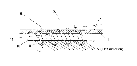
Specific Description of the Drawings
Figure 4 shows a device for non-collinear parametric generation of THz
radiation.
This has a nonlinear crystal 5, which in response to a pump wave 4 generates
parametrically a signal wave 6 and an idler wave 7. To enable coupling of the
generated signal wave 6 from the nonlinear crystal 5, which would otherwise be
totally internally reflected, an array of silicon prisms 9 is provided.
Between the
nonlinear crystal 5 and the array of prisms 9 is a dielectric coating layer
10. This layer
is selected so that it can prevent pump wave 4 and idler wave 7 radiation
scattered
CA 02676674 2009-07-27
WO 2007/088336 8 PCT/GB2007/000295
within the nonlinear crystal 5 from impinging the silicon prism array 9. This
is
provided on an outwardly facing side 11 of the non-linear crystal 5. Any
suitable
material could be used for the filter provided it is able to block or
otherwise prevent
transmission of light into the array at the wavelengths of interest. For
example, where
it is acting as an absorber, the filter may include plastics, paints, ceramics
and papers.
In use, as the pump wave 4 and idler wave 7 propagate through the nonlinear
crystal 5
they are subject to scattering, resulting in a small proportion of the
radiation 15 from
these waves propagating in all directions within the nonlinear crystal 5. Some
of the
scattered radiation impinges the side face 11 of the nonlinear crystal 5 where
it is
substantially blocked from propagating into the silicon prism array 9 by the
single-
layer dielectric coating 10. Hence, the signal wave can be coupled into the
prism
array, whilst free carrier generation is minimised.
As a specific example, the nonlinear crystal 5 is magnesium oxide doped
lithium
niobate (MgO:LiNb03). The pump wave 4 is derived from that class of lasers
based
on the neodymium active ion, for example neodymium yttrium aluminium garnet
(Nd:YAG) having a wavelength of 1064 nanometres. It is usual that the pump
wave 4
is made to propagate along the crystallographic x-axis of the MgO:LiNb03
nonlinear
crystal 5 with polarisation parallel to the crystallographic z-axis and
further that the
generated idler wave 7 propagates within the nonlinear crystal 5 at an angle
of around
0.7 degrees to the pump wave 4 in the x-y crystallographic plane with
polarisation
parallel to the crystallographic z-axis.
For this condition the generated signal wave 6 has a frequency of 1.4 THz and
propagates at an angle of 65 degrees relative to the pump wave 4. Thus for a
nonlinear crystal with sides parallel to the crystallographic x-axis
propagation of the
signal wave 6 is at an angle of 25 degrees relative to the normal of side face
11. This
angle is greater than the total internal reflection angle for a nonlinear
crystal to air
interface, however, the application of the silicon prism array 9 to the side
face 11
allows efficient coupling of the signal wave from the nonlinear crystal into
the silicon
prism array. The silicon prism array 9 is designed so that the signal wave 6
in the
silicon prism array impinges the silicon to air interface 12 at close to
normal
incidence. The prism angle f3 to achieve this is around 43 degrees. Preferably
the
CA 02676674 2009-07-27
WO 2007/088336 PCT/GB2007/000295
9
prism array is fabricated from high resistivity (>10 kohm/cna) silicon so that
the
absorption loss experienced by the signal wave 6 is minimised. By having the
filter
between the non-linear crystal and the array 9, free carrier generation in the
silicon
can be minimised.
5
The above description of a specific embodiment is made by way of example only
and
not for the purposes of limitations. It will be clear to the skilled person
that minor
modifications may be made without significant changes to the operation
described.
For example the coating may be a multi-layer dielectric coating or an
absorbing
10 coating or may be applied to the semi-insulator device or devices or may
be an
appropriate filter, preferably a blocking filter, simply clamped between the
semi-
insulator and first medium from which the em wave originates.