Note : Les descriptions sont présentées dans la langue officielle dans laquelle elles ont été soumises.
CA 02678460 2009-08-14
BTS 08 3 091-Foreign countries
-1-
Mass spectrometer
The invention relates to a mass spectrometer having:
- an ionization chamber with a feed channel for the gas to be examined,
- an electron source for ionizing the gas to be examined,
- electrodes for accelerating the ionizing electrons,
- electrodes for the mass-dependent separation of the ions by
acceleration/deceleration
thereof,
- a detector for the separated ions, and
- a wiring with metallic wires.
Mass spectrometers are used in many kinds of applications. Whereas mass
spectrometers were
formerly used primarily for scientific purposes, nowadays there are more and
more applications in
connection with protection of the environment, measurements of air quality for
detecting harmful
gases, process monitoring and control, security checks e.g. in airports, and
the like. In particular
mass spectrometers which have small dimensions and are therefore easy to
transport and can be
used ubiquitously are suitable for these purposes. For application on a large
scale, a further
requirement is that these mass spectrometers can be produced cost-effectively.
Previously known mass spectrometers having a quadrupole mass separator (WO
2004/013890, GB
234908 A) are distinguished by small size. The disadvantage is that, in the
case of such quadrupole
mass separators, very stringent requirements are made of the electrode
geometry, with the result
that a separator cannot be produced by the etching and deposition methods that
are customary in
microsystems engineering. Since the systems comprise a plurality of components
which have to be
aligned and positioned in an accurately fitting manner with respect to one
another, expensive and
complicated individual system processing is necessary.
In a further mass spectrometer, a magnetic field separator is used (WO
96/16430). However, the
latter requires a certain minimum size since, on the one hand, very high
magnetic field strengths
have to be present for the magnetic field separator, while elsewhere the
magnetic field has to be
shielded in order not to influence the ionization or ion optics.
CA 02678460 2009-08-14
BTS 08 3 091-Foreign countries
-2-
In a mass spectrometer produced according to microsystems engineering (YOON H
J et al:
"Fabrication of a novel micro time-of-flight mass spectrometer", SENSORS AND
ACTUATORS
A, ELSEVIER SEQUOIA S.A., LAUSANNE, CH, Vol. 97-98, 1 April 2002 (2002-04-01),
pages
441-447, XP004361634 (ISSN: 0924-4247), the substrate used is silicon, which
has the advantage
of a great variety of patterning possibilities, but has the disadvantage that
large leakage currents
that heat the substrate flow. A further disadvantage is the high dielectric
constant, which leads to
signal corruptions even if an insulating interlayer composed of silicon
dioxide is used. Moreover,
only a continuous acceleration in the direction of movement takes place, but
not a time-variant
acceleration perpendicular to the direction of movement of the ions through
the electric fields, by
means of which the speed-dependent selection of ions can be improved, with the
result that all the
ions pass to the detector and the measurement of the ion current has to be
temporally resolved. In
addition, the previously known mass spectrometer is not constructed in
complete fashion; separator
and detector are separate elements, as is shown in figure 11.
A further previously known miniaturized mass spectrometer (WO 96/11492) is
likewise not
produced in completely planar fashion by the methods of microsystems
engineering; external
magnets for the mass separation are provided. The corresponding disadvantages
have already been
mentioned above in connection with another known mass spectrometer (WO
96/16340).
A mass spectrometer of the type mentioned in the introduction was developed
for use in a
microsystem that can be produced by the customary methods in microsystems
engineering
(DE 197 20 278 A 1). This mass spectrometer has only very small dimensions.
However,
production is very complex since, on the one hand, said mass spectrometer
requires self-supporting
insulated grids for the acceleration for the ionization of the gas to be
examined and, on the other
hand, it is necessary to produce electrically contact-connected,
electrolytically grown structures
composed of copper and/or nickel. The individual components are constructed
separately on a total
of four substrates, which have to be connected to form a monolithic system by
means of suitable
construction and connection technology.
The object of the invention is to provide a mass spectrometer of the type
mentioned in the
introduction which can be produced simply and cost-effectively and is suitable
for mass
production.
The solution according to the invention consists, in the case of a mass
spectrometer of the type
mentioned in the introduction, in the fact
that it is constructed in completely planar fashion
the components are arranged on a plane nonconductive substrate,
CA 02678460 2009-08-14
BTS 08 3 091-Foreign countries
-3-
that it has an energy filter for the ions, said energy filter being embodied
as a sector, in
particular a 90 sector,
the ionization chamber, the electrodes for accelerating the electrons and
ions, the detector
for the ions and the energy filter are produced by photolithography and
etching of a doped
semiconductor die applied to the substrate and the wiring and the
abovementioned parts are
covered by a second flat nonconductive substrate.
In this case, "sector" should be understood to mean an arc section on which
the ions move.
The function of the mass spectrometer with the mass-dependent separation of
the ions by
acceleration/deceleration is based on the fact that as a result of the
acceleration by the fields of the
electrodes, ions that vary in heaviness attain a differing speed and the
separation is effected on the
basis of these speed differences. However, the corresponding ion beam allowed
through is not
monochromatic, it also contains ions having a larger or smaller mass which had
a higher or lower
starting speed on account of the thermal motion. In order to filter out these
non-monochromatic
ions, the energy filter is provided, in which, between two electrodes having
different, in particular
opposite, potentials, the ions are deflected in a channel (sector) between the
electrodes. A higher
accuracy is obtained by means of this measure.
In contrast to the prior art of a double-focusing mass spectrometer (WO
96/11492) the deflection
by means of external magnetic fields is dispensed with here. In the case of
the invention, the
separation of the ions according to mass/energy is effected only by means of
electric fields that are
generated within the planar structure.
The particular advantage of the invention is that the mass spectrometer is
constructed in completely
planar fashion and can be produced from wafers using the techniques in
microelectronics. The
components are arranged on a plane nonconductive substrate, on which the
metallic connection
wiring has initially been applied. The ionization chamber, the electrodes for
accelerating the
electrons and ions, the detector for the ions and the energy filter are
produced by photolithography
and etching of a semiconductor die applied to the substrate and the wiring,
wherein all the
components are produced in one photolithographic and etching step. Afterward,
the components
are then covered by a flat nonconductive substrate in order thus to obtain a
closed unit.
In one advantageous embodiment, the electron source is a thermal emitter. In
another advantageous
embodiment, the electron source has a plasma chamber with a feed channel for a
noble gas and
with a microwave line for introducing microwaves for generating and
maintaining the plasma,
wherein the plasma chamber, the feed channel and the microwave line are
likewise produced by
etching of the semiconductor die together with the other parts.
CA 02678460 2009-08-14
BTS 08 3 091-Foreign countries
-4-
In one advantageous embodiment, the electrodes for the mass-dependent
separation of the ions by
acceleration/deceleration are embodied and arranged as a time-of-flight mass
separator. The ion
beam is pulsed in a first gate electrode arrangement. In this way, only short
ion pulses pass into the
drift path, where the pulse diverges on account of the different speeds of the
ions. The ion pulse is
sampled at a second gate electrode arrangement. In this case, different
propagation times
correspond to different masses. The energy filter then ensures that only ions
having precisely one
energy reach the detector and are registered there.
In a traveling field separator, in the measurement section a relatively large
number of electrodes are
provided to which electrical (AC) voltages are applied which "travel" from one
end to the other end
with the ions. Only the ions having precisely the speed that corresponds to
the "traveling speed" of
the electric fields always move through electrodes to which no voltage is
being applied. All the
other ions, which are out of step, move between electrodes to which an
electrical voltage is being
applied, with the result that they are deflected to the side.
The detector for the ions is advantageously embodied as a Faraday detector. In
another
advantageous embodiment, which has greater sensitivity, the detector for the
ions is embodied as
an electron multiplier.
The electrodes for accelerating the electrons can be two electrodes which are
provided with screen
openings and to which different electrical potentials can be applied. These
electrodes can likewise
be produced from the semiconductor material, with the result that the
previously known grid
arrangement for accelerating the electrons in the prior art (DE 197 20 278 A),
which is difficult to
produce, is avoided.
The mass spectrometer advantageously has a microcontroller, by means of which
said mass
spectrometer is controlled.
The metallic conductors of the wiring and the electrodes are advantageously
electrically connected
by eutectic semiconductor-metal contacts. For this purpose, bumps composed of
a suitable metal
are arranged on the wires or conductor tracks on the corresponding locations,
said bumps forming
the eutectic semiconductor-metal contacts in the course of bonding with the
semiconductor die.
A particular advantageous metal for the eutectic contacts is gold.
The non-conductive substrates are advantageously composed of borosilicate
glass or quartz glass.
The invention is also distinguished by a method for producing the mass
spectrometer. In
accordance with these methods, the metallic wiring is applied to a flat
nonconductive substrate,
CA 02678460 2009-08-14
BTS 08 3 091 -Foreign countries
-5-
metal pads for connection to the semiconductor electrodes being arranged on
said wiring.
Depressions corresponding to the wiring are then etched into the semiconductor
die in order that
the semiconductor material comes into contact only with the metal pads but not
with the wiring
during bonding. Afterward, the semiconductor die is then applied to the
substrate and a mask for
photolithography is arranged onto the same. In this case, the alignment of the
mask with respect to
the wiring and gold pads can be effected optically by using light having a
wavelength for which the
silicon die is transparent. For silicon, a wavelength above 1.2 m is suitable
in this case. After
corresponding exposure and removal of the mask, the semiconductor die is then
etched locally in
one step, in order to produce the components of the mass spectrometer. The
semiconductor die is
subsequently covered with a second nonconductive substrate.
In this case, a further wiring can be applied to the second nonconductive
substrate beforehand in
order e.g. to connect electrodes of electrode pairs to one another.
The invention is described below on the basis of advantageous embodiments with
reference to the
accompany drawings, in which:
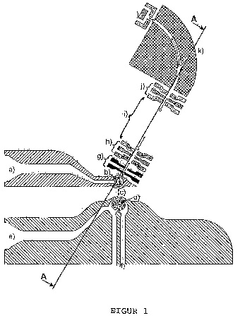
Figure I shows the basic arrangement of the essential parts of an advantageous
embodiment of
the mass spectrometer without wiring and non conductive substrates;
Figure 2 shows a section along the line A-A from figure 1, the nonconductive
substrates being
concomitantly illustrated.
Figure 3 shows another embodiment, in an illustration similar to figure 1;
Figure 4 shows a section corresponding to the line A-A from figure 3, in an
illustration similar
to figure 2;
Figure 5 and figure 6 show illustrations of a third embodiment corresponding
to figures 1 and 2,
and figures 3 and 4;
Figure 7 shows a plan view of the accelerating electrode arrangement;
Figure 8 shows a section along the line A-A from figure 7; and
Figure 9 shows the principle of the production of the mass spectrometer of the
invention.
Figure 1 shows the finished semiconductor die, which is composed of doped
silicon in this
embodiment and in which the corresponding components are produced by etching.
The
CA 02678460 2009-08-14
BTS 08 3 091 -Foreign countries
-6-
spectrometer has a feed channel a for the sample gas that is conducted into
the ionization chamber
b. The electrons having an energy of typically 70 eV which are required for
the ionization are
extracted from a plasma chamber d and accelerated between two screen openings
c, which are at
different potentials. The entire region between the screen openings is
evacuated toward the sides of
the system. The noble gas is fed to the plasma chamber d via the channel e. It
is excited with
microwaves via the microwave conductor f in order to generate the plasma and
thereby liberate the
electrons required. Pressure in the plasma chamber is controlled by means of
the inlet pressure
upstream of the channel e or a connected capillary.
The ions from the ionization chamber b are extracted by an electric field
between chamber wall and
ion optics g to a further screen opening, and with a defined energy are
accelerated and focused. The
ion beam is pulsed at the first gate electronic arrangement h. Consequently,
only short ion pulses
pass into the drift path i, where the pulse diverges on account of the
different speeds of the ions.
The ion pulse is sampled at the second money electrode arrangement j. The
energy filter k ensures
that ions only having precisely one energy reach the detector I and are
registered there.
Figure 3 and 4 show another embodiment, which differs from the embodiment in
figures 1 and 2 in
the region of the accelerating electrodes. An AC voltage is applied to the
electrodes m of the
traveling field separator, with the result that ions moving through between
electrodes to which a
voltage is being applied are deflected to the side and removed from the beam.
Only the ions having
precisely the correct speed which in each case pass through the electrodes
when there is no voltage
present at the latter reach the energy filter k, the two electrodes of which
on both sides of the
quadrant-shaped channel are at opposite potentials, in order thus to allow
through only ions having
a precisely defined energy. These ions then again impinge on the detector I.
The embodiment in figures 5 and 6 differs from that in figures 1 and 2 in
that, instead of a noble
gas plasma, a thermal emitter n is used for liberating the electrons required
for the ionization.
Figures 7 and 8 show the electrode region of the mass spectrometer according
to the invention. The
borosilicate glass I serves as a carrier for the system, metallic conductor
tracks 2 being applied to
said borosilicate glass in order to electrically interconnect the electrodes.
The electrical contact
between the metallic conductor tracks 2 and the silicon electrodes 4 is
effected by means of a
eutectic gold-silicon contact 5. Gold pads 3 at the contact locations between
conductor track 2 and
silicon electrode 4 alloy in the course of bonding with the highly doped
silicon and thus produce an
ohmic contact. In this case, the construction of the electrodes is shown in
section in figure 8.
Figure 9 shows the principle of the production of the mass spectrometer.
Cutouts 8 are produced by
means of an etching in the silicon die, said cutouts providing for the
required distance between the
metallic conductor tracks 2 on the carrier substrate I and the silicon die 6
in the finished mass
CA 02678460 2009-08-14
BTS 08 3 091-Foreign countries
-7-
spectrometer. This is necessary in order that the substrate 1 and the silicon
die 6 can be bonded in
planar fashion. In this case, the depth of the etching pits 8 is designed such
that the gold pads 3
come into contact with the bottom of the etching pit 8 when substrate 1 and
silicon die 6 are joined
together. The arrangement thus produced in accordance with I is then bonded in
step II. In step 111,
the desired structure is produced after application of a corresponding mask
and exposure by
etching. The upper substrate 7 shown in I, 11 and III is in reality not yet
present during these steps.
It likewise bears a conductor and is then bonded onto the arrangement during
IV, wherein
electrodes are connected by the conductor arranged on the upper substrate 7.
The production of the mass spectrometer can be effected in uniform steps in
wafers. The finished
mass spectrometer shown in the figures can have dimensions of as small as 5x10
mm. On account
of the small size, the requirements made of the pump capacity of a vacuum pump
are only low as
well.