Note : Les descriptions sont présentées dans la langue officielle dans laquelle elles ont été soumises.
CA 02680450 2009-09-10
WO 2008/112234 PCT/US2008/003241
DETONATOR IGNITION PROTECTION CIRCUIT
BACKGROUND OF THE INVENTION
[0001 ] The present invention relates to electric and electronic detonators
and, more spe-
cifically, to such detonators being protected against inadvertent firing by
stray or induced electri-
cal currents, magnetic fields and the like.
[0002] U.S. Patent 5,179,248 (the `248 patent), issued January 12, 1993 to J.
Keith Hart-
man et al. and entitled "Zener Diode For Protection Of Semiconductor Explosive
Bridge", dis-
closes protection of a semiconductor bridge against inadvertent firing by
connecting a zener di-
ode across the conductive metal lands forming part of the semiconductor
bridge. As explained at
column 3, line 14 et seq., a semiconductor bridge device includes a pair of
spaced-apart metal
lands disposed in ohmic contact on a doped semiconductor layer with a gap
between the lands.
In response to a voltage or current equal to or in excess of a predetermined
level and duration
being applied to the gap between the lands, a plasma is formed in the gap with
sufficient energy
to initiate an explosive disposed in the gap. The device for preventing
accidental discharge in-
cludes and preferably consists of a zener diode having anode and cathode
electrodes respectively
connected to the first and second lands of the semiconductor bridge device.
[0003] U.S. Patent 5,309,841 (the `841 patent), issued May 10, 1994 to J.
Keith Hartman
et al. and entitled "Zener Diode For Protection of Integrated Circuit
Explosive Bridge", expands
on the disclosure of the '248 Patent, including disclosure of circuits adding
a capacitor and en-
ergy source in parallel with the zener diode and incorporating the elements
into an integrated cir-
cuit.
[0004] As disclosed in both the `248 patent (col. 6, line 56 through col. 7,
line 7; Fig. 3)
and the `841 patent (col. 7, lines 20-39; Fig. 3), protection against
premature firing of the semi-
conductor explosive bridge is accomplished via waveform clipping by the
protective zener diode.
[0005] While existing protective schemes for detonator devices may be suitable
for their
intended purpose, there remains, however, a need in the art for improved
protective schemes that
CA 02680450 2009-09-10
WO 2008/112234 PCT/US2008/003241
2
provide improved protection against possible stray voltage conditions that
could cause unplanned
initiation of a detonator.
BRIEF DESCRIPTION OF THE INVENTION
[0006] An embodiment of the invention includes an ignition circuit for a
detonator in-
cluding; an igniter having a first terminal and an opposing second terminal, a
first diode electri-
cally connected in series with the igniter at the first terminal, and a second
diode electrically
connected in series with the igniter at the second terminal. The first and
second diodes each have
an anode terminal and a cathode terminal, wherein like terminals of the first
and second diodes
are electrically connected to the igniter, thereby defining proximal terminals
proximate the ig-
niter and distal terminals on an opposing side of each respective diode. An
energy source and a
switch are electrically connected in series with each other, and are
electrically connected across
the distal terminals. Current flow through the igniter sufficient to ignite
the igniter is prevented
until an ignition voltage is applied to the distal terminals that is equal to
or greater than the re-
verse breakdown voltage of the first diode or the second diode.
BRIEF DESCRIPTION OF THE DRAWINGS
[0007] Referring now to the drawings, which are meant to be exemplary and not
limiting,
and wherein like elements are numbered alike in the accompanying Figures:
[0008] Figure 1 depicts in cross-sectional schematic view a detonator shell
for use in ac-
cordance with an embodiment of the invention;
[0009] Figure 2 depicts a schematic of an exemplary firing circuit in
accordance with an
embodiment of the invention; and
[0010] Figure 3 depicts an alternate igniter to that depicted in Figure 2 for
use in accor-
dance with an embodiment of the invention.
DETAILED DESCRIPTION OF THE INVENTION
[0011 ] An embodiment of the invention, as shown and described by the various
figures
and accompanying text, provides a protection scheme for preventing unplanned
initiation of a
CA 02680450 2009-09-10
WO 2008/112234 PCT/US2008/003241
3
detonator that may be used for seismic exploration, oil/gas well stimulation,
or blasting in haz-
ardous environments, while providing sufficient ignition voltage to an igniter
upon command
without substantially increasing the amount of energy that an energy source
must be capable of
delivering to the detonator for delayed ignition.
[0012] Referring to Figure 1, an exemplary detonator 100 is depicted in cross-
sectional
schematic view having a detonator shell 105 that houses an input connector 110
having input
pins 115 and output pins 120, a protection circuit 125 (to be discussed in
more detail below with
reference to Figure 2), an output connector 130 having input pins 135 and
output pins 140, an
ignition region 145, a first stage detonator charge 150, a second stage
detonator charge 155, and
a third stage detonator charge 160. Receipt of a planned ignition voltage at
input pins 115 is
transferred to protection circuit 125 via output pins 120, which properly
passes through protec-
tion circuit 125 in a manner to be discussed in more detail below to cause a
chain reaction start-
ing with ignition of an igniter 210 (discussed below with reference to Figure
2) disposed within
ignition region 145, which in succession causes firing of the first stage
detonator charge 150, the
second stage detonator charge 155, and then the third stage detonator charge
160. In an em-
bodiment, the detonator shell 105 is standard commercial detonator shell
having a 0.25 inch (6.5
mm) nominal diameter opening, the first stage detonator charge 150 is diazo
(diazo dinitro phe-
nol, usually referred to as DDNP), the second stage detonator charge 155 is
loose PETN (pentae-
rythritol tetranitrate, also known as penthrite), and the third stage
detonator charge 160 is pressed
PETN.
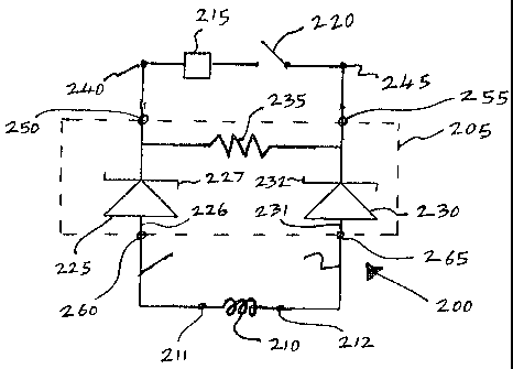
[0013] Referring now to Figure 2, an exemplary ignition circuit 200 is
depicted having
protection circuit 205, an igniter 210 having first 211 and second 212
terminals, a source of elec-
trical energy 215, and a switch 220. In an embodiment, protection circuit 205
includes a first
diode 225 having anode 226 and cathode 227, a second diode 230 having anode
231 and cathode
232, and an optional resistor 235. As illustrated, first diode 225 is
electrically connected in se-
ries with igniter 210 at first terminal 211, and second diode 230 is
electrically connected in series
with igniter 210 at the opposing second terminal 212, wherein like terminals
(anodes 226 and
231 for example) of the first and second diodes 225, 230 are electrically
connected to the igniter
210, thereby defining proximal terminals proximate the igniter and distal
terminals on an oppos-
CA 02680450 2009-09-10
WO 2008/112234 PCT/US2008/003241
4
ing side of each respective diode. As also illustrated, energy source 215 and
switch 220 are elec-
trically connected in series with each other, and electrically connected
across the distal terminals
of first and second diodes 225, 230.
[0014] In relating Figure 2 to Figure 1, contact points 240, 245 in Figure 2
are electri-
cally synonymous with input pins 115 in Figure 1, contact points 250, 255 in
Figure 2 are elec-
trically synonymous with output pins 120 in Figure 1, contact points 260, 265
in Figure 2 are
electrically synonymous with input pins 135 in Figure 1, and terminals 211,
212 in Figure 2 are
electrically synonymous with output pins 140 in Figure 1. While not
specifically depicted in
Figure 1, it will be appreciated by the description and illustration disclosed
herein that the energy
source 215 and switch 220 illustrated in Figure 2 are connected to pins 115 of
detonator 100 in
Figure 1 (synonymous with contact points 240, 245 of Figure 2), thereby
providing the necessary
energy, switching means and ignition voltage to fire igniter 210 disposed in
ignition region 145.
In an embodiment, energy source 215 is a battery, a charged capacitor, or any
other energy
source suitable for the purposes disclosed herein, and switch 220 is an
electronic switching de-
vice, or any other switching device suitable for the purposes disclosed
herein, where switch 220
is a separate component or integrated within a time delay module.
[0015] As mentioned above, resistor 235 may be optionally disposed in
electrical connec-
tion across the distal terminals of diodes 225, 230, and in parallel with the
series-connected en-
ergy source 215 and switch 220. When present, resistor 235 provides an
electrical path in front
of the diodes 225, 230 for pre-testing the integrity of electrical connections
from the firing sta-
tion (not illustrated) up to the protection circuit 205 and igniter 210, and
for protecting the circuit
205 against stray static voltages.
[0016] In accordance with an embodiment of the invention, current flow through
igniter
210 sufficient to ignite igniter 210 is prevented until an ignition voltage is
applied to the distal
terminals (250, 255 for example) of diodes 225, 230 that is equal to or
greater than the reverse
breakdown voltage of the first diode 225 or the second diode 230.
[0017] In an embodiment, the first and second diodes 225, 230 are zener diodes
having
the same reverse breakdown voltage rating of 20 Volts, and are disposed such
that their anodes
226, 231 are the proximal terminals (that is, anodes 226, 231 are electrically
connected to igniter
CA 02680450 2009-09-10
WO 2008/112234 PCT/US2008/003241
210). In another embodiment, first and second diodes 225, 230 are zener diodes
having the same
reverse breakdown voltage rating of 200 Volts.
[0018] In an embodiment, igniter 210 is a bridgewire designed for contact with
(for ex-
ample, to be embedded within) an explosive device (for example, the first
stage detonator charge
150) with a pair of lead wires extending from the bridgewire. However, it will
be appreciated
that other igniters suitable for the purposes disclosed herein may be employed
in place of the
bridgewire, such as a semiconductor bridge 300 for example, generally depicted
in Figure 3, hav-
ing lands 305, 310 in electrical contact with a semiconductor layer 315, all
disposed on a sub-
strate 320, with the first stage detonator charge 150 being disposed across
lands 305, 310 and
semiconductor layer 315. Operation of such a semiconductor bridge 300 in the
field of explosive
detonators is well known in the art and is not discussed further herein.
[0019] In an embodiment, first diode 225, second diode 230, and optional
resistor 235 are
all surface mounted on a circuit board, generally depicted by reference
numera1205 and the as-
sociated dashed-line graphical box depicted in Figure 2. The combination of
circuit board 205
with surface-mounted diodes 225, 230 and resistor 235 (collectively referred
to as surface-
mounted components) is so dimensioned as to be insertable through the space
defined by the
opening of detonator shell 105, which in an embodiment is a standard
commercial detonator
shell having a 0.25 inch (6.5 mm) nominal diameter opening. When the circuit
board with sur-
face-mounted components is positioned within the detonator shell, the
dielectric breakdown volt-
age between any of the surface-mounted components and the interior wall of the
detonator shell
is greater than the reverse breakdown voltage of each of the first diode 225
and the second diode
230.
[0020] Upon closure of the switch 220 (planned ignition), not only does the
energy
source 215 have sufficient energy to generate a voltage at the distal
terminals 250, 255 in excess
of the reverse breakdown voltage of the first diode 225 or the second diode
230 to generate suffi-
cient current flow to ignite the igniter 210, but also the energy source 215
further has sufficient
energy to permanently damage a reverse-biased one of the first and second
diodes 225, 230.
Since the detonator 100 is an intended self-destructive device, there is no
need for either diode
225, 230 to be designed for passing a reverse-biased current without damage
thereto. As such,
CA 02680450 2009-09-10
WO 2008/112234 PCT/US2008/003241
6
diodes having a reverse-biased current rating far below the actual current
passed are fully suffi-
cient for the purposes disclosed herein, thereby permitting small diodes to be
used in a compact
design for the protection circuit 205.
[0021 ] In an embodiment and in the event of the switch 220 being closed, the
energy
source 215 has sufficient energy to generate an ignition voltage to ignite the
igniter 210 that is
equal to or greater than 1.1 times the reverse breakdown voltage of either of
the first diode 225
and the second diode 230. And, in the event of the switch 220 being open, each
of the first 225
and second 230 diodes have a reverse breakdown voltage sufficient to prevent
the igniter 210
from firing upon the occurrence of a stray voltage at the distal terminals
(250, 255 for example)
less than the reverse breakdown voltage of the associated reverse-fed diode.
[0022] While embodiments of the invention have been described herein employing
a cir-
cuit board 205 with diodes 225, 230 and resistor 235 surface-mounted thereon,
it will be appreci-
ated that other packaging arrangements can be employed for the purposes
disclosed herein, such
as integrally molding diodes 225, 230 and resistor 235 into a plug, again
generally depicted by
reference numeral 205 and the associated dashed-line graphical box depicted in
Figure 2, where
the plug 205 with the integrally-molded diodes 225, 230 and resistor 235 is so
dimensioned as to
be insertable through the space defined by the opening of a standard size 0.25
inch (6.5 mm) di-
ameter detonator shell 105.
[0023] While embodiments of the invention have been described herein having
anodes
226, 231 of first diode 225 and second diode 230, respectively, being
connected to igniter 210, it
will be appreciated that the scope of the invention also covers an arrangement
where both diodes
are reversed such that their cathodes 227, 232 are connected to igniter 210,
as long as both di-
odes are oriented in the same direction such that no current will flow through
igniter 210 if an
unplanned voltage below the diode breakdown voltage is applied across the
contact points 250,
255 of circuit 205.
[0024] An example of the circuit illustrated in Figure 2 was built utilizing
20-volt zener
diodes for diodes 225 and 230, a 68 kilo-ohm resistor for resistor 235, and a
standard bridgewire
utilized in a superseismic detonator manufactured by Dyno Nobel Inc. of Salt
Lake City, Utah,
for igniter 210.
CA 02680450 2009-09-10
WO 2008/112234 PCT/US2008/003241
7
[0025] A series of tests were conducted in which different levels of voltages
were applied
to the circuit across contact points 240, 245. All of the tests were carried
out by supplying power
(energy source 215 for example) from a 250 micro Farad capacitor charged to
the voltage speci-
fied in Table-1 below, which tabulates the test results.
Table-1
Voltage (in Volts)
Test No. Did Not Fire Fired
1 10 36
2 15, 19 24
3 10, 15, 19 22
4 19, 19.8, 20.5 28
19 22
6 19.5, 20, 21.7 22
7 21 22
8 21 22
9 21, 21.7 29.5
20,21,21.7 21.9
[0026] As shown by the data of Table-1, application of test voltages below, or
even
slightly in excess of, the 20-volt rating of the zener diodes precluded firing
of the bridgewire.
For example, voltages as high as 19 volts (tests 2 and 3), 19.8 and 20.5 volts
(test 4), 19.5, 20
and 21.7 volts (test 6) and 20, 21 and 21.7 volts (tests 7-10) all failed to
fire the bridgewire. On
the other hand, voltages more significantly above the 20-volt rating of the
zener diode provided
consistent firing. For example, tests 3 and 5-8 showed firing at 22 volts.
Test 10, which showed
no firing at 21.7 volts, showed that firing occurred at 21.9 volts.
Significantly higher voltages
such as 36 volts (test 1) and 29.5 volts (test 9) were successful. The test
data clearly show the
CA 02680450 2009-09-10
WO 2008/112234 PCT/US2008/003241
8
reliability of the zener diode protecting the bridgewire from firing even at
voltages as high as
21.7 volts.
[0027] Because diodes 225 and 230 are oriented in the same direction as
illustrated in
Figure-2, that is, the diodes face each other in their forward directions,
current flow is precluded
by a voltage applied across the circuit at contact points 240, 245, until and
unless the voltage ex-
ceeds the breakdown voltage of the diodes. Once the breakdown voltage is
exceeded, current
would then flow to energize the bridgewire.
[0028] If zener diodes are utilized as the diodes 240, 245, their breakdown
voltage can be
precisely specified and a specific all fire/no fire value can readily be
established for the diode-
protected detonator by utilizing methods and calculations well known to those
skilled in the art.
As discussed above, the facing diodes, for example, facing zener diodes,
together with the other
circuit components, can readily be positioned on a small board or molded into
a plug, either of
which will readily fit into the inside diameter, about 0.25 inches (6.5 mm),
of a standard com-
mercial detonator shell. The disclosed detonator is resistant to stray current
engendered by radio
frequency energy, static and any other electrical power that does not exceed
the diode breakdown
voltage.
[0029] It is contemplated that in an embodiment where first and second diodes
225, 230
are zener diodes each having a reverse breakdown voltage of 200 Volts,
sufficient protection of
igniter 210 will be provided against a standard 120 VAC-rms voltage at input
pins 115 having a
peak voltage of about 170 Volts. By employing zener diodes having a 200 Volt
reverse break-
down voltage (first and second diodes 225, 230 in the contemplated embodiment)
and a very
small current rating (less than 2 milliamps for example), a massive energy
pulse of 4-8 joules
from a 400 Volt capacitor discharge firing system will result in a one-time
use of diodes 225,
230, which will fail in conduction mode. Since diodes 225, 230 need to work
only once, such an
occurrence of failure in the conduction mode is perfectly acceptable for the
purposes disclosed
herein. An exemplary commercially available zener diode suitable for the
purposes disclosed
herein is part number 1 SMB5956BT3G manufactured by Oakley Telecom, LC, having
a nominal
reverse zener voltage of 200 volts at a reverse current of 1.9 milliamps.
CA 02680450 2009-09-10
WO 2008/112234 PCT/US2008/003241
9
[0030] The accuracy of the timing of initiation of individual explosive
charges in a mul-
tiple-charge blasting system must be closely controlled to achieve the desired
fragmentation of
ore and rock, and to reduce the influence of the blast on structures outside
the blast zone. The
accuracy of timing of the initiation of individual charges controls the
effectiveness of the blast by
providing the required distribution of blast induced shockwaves. Embodiments
of the invention
provide detonators that can be used for closely controlling the timing of the
initiation of individ-
ual explosive charges in multiple-explosive charge blast operations. For
example, for electronic
delay of detonator 100, the test voltage provided to contact points 250, 255
of ignition circuit 200
could be safely raised to a level just below the breakdown voltage of diodes
225, 230 without
concern of prematurely firing the very low energy igniter 210, thereby
enabling better communi-
cation with other connected detonators within the multiple-charge blasting
system. Additionally,
and contrary to other blasting systems that employ a series-connected resistor
to protect the ig-
niter, which inherently results in an 12 R power loss across the series-
connected resistor during
ignition, embodiments of the invention do not have such a power loss and
therefore have more
energy available from energy source 215 for use by electronic delay circuitry,
communications,
and controls of the blasting system.
[0031 ] While the invention has been described with reference to exemplary
embodi-
ments, it will be understood by those skilled in the art that various changes
may be made and
equivalents may be substituted for elements thereof without departing from the
scope of the in-
vention. In addition, many modifications may be made to adapt a particular
situation or material
to the teachings of the invention without departing from the essential scope
thereof. Therefore, it
is intended that the invention not be limited to the particular embodiment
disclosed as the best or
only mode contemplated for carrying out this invention, but that the invention
will include all
embodiments falling within the scope of the appended claims. Also, in the
drawings and the de-
scription, there have been disclosed exemplary embodiments of the invention
and, although spe-
cific terms may have been employed, they are unless otherwise stated used in a
generic and de-
scriptive sense only and not for purposes of limitation, the scope of the
invention therefore not
being so limited. Moreover, the use of the terms first, second, etc. do not
denote any order or
importance, but rather the terms first, second, etc. are used to distinguish
one element from an-
CA 02680450 2009-09-10
WO 2008/112234 PCT/US2008/003241
other. Furthermore, the use of the terms a, an, etc. do not denote a
limitation of quantity, but
rather denote the presence of at least one of the referenced item.