Note : Les descriptions sont présentées dans la langue officielle dans laquelle elles ont été soumises.
CA 02680468 2009-09-10
WO 2008/112598 PCT/US2008/056349
METHOD FOR UTILIZING HEAVILY DOPED SILICON FEEDSTOCK TO PRODUCE
SUBSTRATES FOR PHOTOVOLTAIC APPLICATIONS BY DOPANT COMPENSATION
DURING CRYSTAL GROWTH
[0011 CROSS-REFERENCE TO RELATED APPLICATIONS
[ 0 021 This application is a continuation-in-part patent application of non-
provisional patent
application 11/684,599 filed March 10, 2007 and claims the benefit of
provisional patent
application 61/016,049, filed December 21, 2007, the disclosure of each of
which is hereby
incorporated by reference herein.
[ 0 031 BACKGROUND OF THE INVENTION
[ 0 041 Field of the Invention
[ 0 051 This invention relates to the manufacture of photovoltaic solar cells.
More
particularly, this invention relates to methods for utilizing heavily doped
silicon feedstock to
produce substrates for photovoltaic applications by dopant compensation during
crystal growth.
[ 0 0 6] Description of the Background Art
[ 0 071 Photovoltaic (PV) devices for producing electrical energy directly
from sunlight have
become increasingly popular in recent years. Worldwide production of PV cells
in 2005
exceeded 1,500 MW, with power output determined under standard test conditions
(1 kW/m2
light intensity, Air Mass 1.5 Global spectrum, and cell at 25 C). With these
solar cells typically
encased in a module having a selling price of approximately $5/W, the 1,500 MW
production
represents a$7.5B/year industry. Furthermore, the worldwide industry output,
measured in
MW/year, has a compounded annual growth rate in excess of 30%. Silicon solar
cells comprise
more than 90% of the market.
-1-
CA 02680468 2009-09-10
WO 2008/112598 PCT/US2008/056349
[ 0 0 8] The starting silicon wafer represents over half the cost of a
completed silicon solar cell.
This high cost is not due to the unavailability of silicon, since silicon is
the second most
abundant element in the earth's crust, behind only oxygen. Rather, it is due
to the high cost of
purifying silicon to a level required for semiconductor applications,
including PV, which is
typically in the parts-per-billion (ppb) range. It is particularly important
to have high purity
levels of silicon with respect to transition metals (e.g., iron, titanium,
vanadium, molybdenum,
tungsten). It is equally important to have high purity levels of silicon with
respect to atoms from
Group III (e.g., boron, aluminum, gallium) and Group V (e.g., phosphorus,
arsenic) in the
Periodic Table of the Elements which serve as p-type and n-type dopants,
respectively, in silicon.
Some silicon purification processes are quite effective in reducing the
concentration of transition
metals to an acceptable level, but are not sufficiently effective in reducing
the dopant atoms to an
acceptable level.
[ 0 0 9] It is an object of this invention to provide an improvement which
overcomes the
aforementioned inadequacies of the prior art methods for purifying silicon and
provides an
improvement which is a significant contribution to the advancement of the art
of manufacturing
solar cells.
[00101 Another object of this invention is to provide a method for using
relatively low-cost
silicon with low metal impurity concentration but contains a high dopant
impurity concentration
for solar cell substrates.
[00111 Another object of this invention is to provide a method for using
relatively low-cost
silicon with low metal impurity concentration by adding a measured amount of
dopant (e.g., one
or more p-type or n-type dopants), before and/or during silicon crystal growth
so as to nearly
-2-
CA 02680468 2009-09-10
WO 2008/112598 PCT/US2008/056349
balance, or compensate, the p-type and n-type dopants in the crystal, thereby
controlling the net
doping concentration within an acceptable range for manufacturing high
efficiency solar cells.
[00121 Another object of this invention is to provide a method for
compensating silicon
feedstock having a dopant concentration to produce solar grade silicon,
comprising the steps of
calculating an initial compensating dopant based upon the dopant concentration
to produce a
desired resistivity, adding the initial compensating dopant to the silicon
feedstock and then
melting and directionally solidifying the silicon feedstock to achieve the
desired resistivity over
at least a portion of an ingot produced from the silicon feedstock.
[00131 Another object of this invention is to provide a method for
compensating silicon
feedstock having a dopant concentration to produce solar grade silicon,
comprising the steps of
calculating an initial compensating p-type dopant or dopants based upon the
dopant
concentration to produce a desired resistivity, adding the initial
compensating p-type dopant or
dopants (e.g., gallium or a gallium alloy) to the silicon feedstock, or during
melting of the
feedstock, and then directionally solidifying the silicon feedstock to achieve
the desired
resistivity over a substantial portion of an ingot produced from the silicon
feedstock, thereby
increasing the yield.
[00141 Another object of this invention is to provide a method for
compensating silicon to
produce solar grade silicon for solar cells, comprising the steps of analyzing
the silicon feedstock
for elements that behave as p type dopants or n type dopants and determining
their initial
concentrations; based upon the initial concentrations the p type dopants and n
type dopants,
calculating the necessary amount of compensating dopant required to achieve a
desired
resistivity range over at least a portion of the solar grade silicon; adding
the compensating dopant
-3-
CA 02680468 2009-09-10
WO 2008/112598 PCT/US2008/056349
to the silicon feedstock; and melting and directionally solidify said
feedstock to achieve the
desired resistivity over at least a portion of the solar grade silicon.
[00151 Another object of this invention is to provide a method for
compensating excessively
doped silicon while in a melt, comprising the steps of: (1) adding an initial
amount of
compensating dopant to the excessively doped silicon while in the melt to
initially compensate
the excessively doped silicon in the melt to an approximate initially-
compensated resistivity; (2)
sampling the initially compensated doped silicon while in the melt to measure
its initially-
compensated resistivity; (3) computing a second amount of compensating dopant
needed to
added to the initially compensated doped silicon while in the melt to
compensate the initially-
compensated silicon in the melt to an approximate second-compensated
resistivity; and (4)
adding the second amount of compensating dopant to the initially compensated
silicon in the
melt.
[00161 Another object of this invention is to provide a method for
compensating silicon to
produce solar grade silicon, comprising the steps of: analyzing the silicon
feedstock for dopant
concentrations, calculating the necessary compensating dopant required to
produce the desired
resistivity during directional solidification, and melting said feedstock and
adding the
compensating dopant during directional solidification to achieve the desired
resistivity.
[00171 Another object of this invention is to provide a method for
compensating silicon to
produce solar grade silicon, comprising the steps of: analyzing the silicon
feedstock for dopant
concentrations; calculating the necessary compensating dopant required to
produce the desired
resistivity during directional solidification; and melting said feedstock and
adding the
compensating dopant during directional solidification to permit flipping from
n type to p type
and to preclude return flipping from p type to n type, or visa versa.
-4-
CA 02680468 2009-09-10
WO 2008/112598 PCT/US2008/056349
[00181 Another object of this invention is to provide a silicon in the form of
a silicon ingot,
sheet, a silicon ribbon or a silicon wafer for solar cells manufactured in
accordance with one of
the methods of the invention.
[00191 Another object of this invention is to provide a silicon in the form of
a silicon ingot,
sheet, a silicon ribbon or a silicon wafer for solar cells comprising both p
and n type dopant
whereby the difference between the p and n type dopants results in a
resistivity between about
0.1 and 10 ohm-cm or more preferably between about 0.5 and 3 ohm-cm.
[00201 The foregoing has outlined some of the pertinent objects of the
invention. These
objects should be construed to be merely illustrative of some of the more
prominent features and
applications of the intended invention. Many other beneficial results can be
attained by applying
the disclosed invention in a different manner or modifying the invention
within the scope of the
disclosure. Accordingly, other objects and a fuller understanding of the
invention may be had by
referring to the summary of the invention and the detailed description of the
preferred
embodiment in addition to the scope of the invention defined by the claims
taken in conjunction
with the accompanying drawings.
[ 0 0 21 ] SUMMARY OF THE INVENTION
[00221 For the purpose of summarizing this invention, this invention comprises
methods for
utilizing heavily doped silicon feedstock to produce substrates for
photovoltaic applications by
dopant compensation during crystal growth.
[00231 By way of background, compensation dopants impact the material
properties of the
silicon substrate including the minority carrier lifetime and diffusion
constant. The most
important material property for solar cells is lifetime, which is the average
time that a
photogenerated electron remains free (in the conduction band) before it
returns to a bound state
-5-
CA 02680468 2009-09-10
WO 2008/112598 PCT/US2008/056349
(in the valence band) by recombining with a hole. It is within this lifetime
period that the
electron must be collected by the internal action of the solar cell in order
for the electron to
contribute to the flow of electrical current from the cell.
[00241 Lifetime is determined by the rate at which photogenerated electrons
and holes
recombine, as described by the Shockley-Read-Hall (SRH) expression. (See, for
example, D. L.
Meier, J. M. Hwang, and R. B. Campbell, "The Effect of Doping Density and
Injection Level on
Minority Carrier Lifetime as Applied to Bifacial Dendritic Web Silicon Solar
Cells," IEEE
Transactions on Electron Devices, volume ED-35, pages 70-79, 1988.) This
recombination rate
depends only on net doping concentration, not on total doping concentration.
This means, for
example, that a silicon wafer with a given level of structural and chemical
defects will have the
same excess (photogenerated) carrier lifetime whether the p-type doping level
is 1 x 10¹⁶ B/cm3
(single dopant) or 10 x 1016 B/cm3 and 9 x 10¹⁶ P/cm3 (compensating p-type and
n-type
dopants), with a net p-type doping density of 1 x 1016 cm 3 and a total doping
density of
19 x 1016 cm 3. Thus, the SRH expression shows there is no lifetime penalty
associated with
compensated silicon relative to uncompensated silicon for the same net doping
density. In
addition, the SRH expression also shows that lifetime generally increases as
the net doping
density decreases. Improved lifetime can therefore be achieved in accordance
with this invention
by partially compensating heavily-doped silicon in order to reduce the net
doping density.
[ 0 0 2 5] The second important material property of the silicon substrate is
the diffusion constant
for photogenerated minority carriers. The diffusion constant is important
because minority
carriers must, during their lifetime, move by diffusion from where they are
created within the
silicon wafer to (typically) the front region of the solar cell. There, the
built-in electric field
associated with the p-n junction collects the minority carriers. A high
diffusion constant is
-6-
CA 02680468 2009-09-10
WO 2008/112598 PCT/US2008/056349
desirable so the minority carriers can move quickly to the collecting region.
Unlike lifetime, the
diffusion constant may be determined by the total doping concentration rather
than the net
doping concentration.
[00261 In compensated silicon, all dopant impurity atoms are ionized (donor
ions have a
positive charge and acceptor ions have a negative charge), so that carriers
(electrons and holes)
are scattered by all dopants. Thus, some penalty is paid in solar cell
efficiency for having
compensated silicon rather than uncompensated silicon. (Efficiency is defined
as the ratio of
electrical power out of the cell to light power incident on the cell.)
[ 0 0 2 7] For example, if silicon is doped p-type to 1 ohm-cm (typical of
current multicrystalline
silicon cell technology) using only boron as the dopant (1.43 x 10¹⁶ B/cm3),
the diffusion
constant for minority carrier electrons is 31.3 cm2/s. If, on the other hand,
silicon is doped
p-type to 1 ohm-cm by compensating a high concentration of boron (14.30 x 10¹⁶
B/cm) with a
somewhat lower concentration of phosphorus (12.87 x 10¹⁶ P/cm3), the diffusion
constant for
electrons is reduced to 13.8 cm2/s. If a lifetime of 15 s is assumed, the
electron diffusion length
for uncompensated 1 ohm-cm silicon is 217 m, while the diffusion length for
compensated
1 ohm-cm silicon is 144 m, where diffusion length is given by (diffusion
constant x lifetime)1z.
For this example, the efficiency calculated by finite element model PC1D is
14.0% for the
uncompensated silicon (Js, of 30.6 mA/cm2 and Vo, of 0.605 V) while the
efficiency calculated
for the compensated silicon is 13.4% (Js, of 29.6 mA/cm2 and Vo, of 0.595 V).
Thus, the
approximate efficiency penalty for compensated silicon, coming not from
lifetime but from
diffusion constant, is approximately 0.6% (absolute) where the majority doping
concentration is
times the net doping concentration. Of course, in cases where the majority
doping is less than
10 times the net doping, the efficiency penalty is less. In an extreme case
where the majority
-7-
CA 02680468 2009-09-10
WO 2008/112598 PCT/US2008/056349
doping compensation is 100 times the net doping concentration, the diffusion
constant for
electrons is reduced to 7.2 cm2/s and the efficiency is calculated to be 12.8%
(Js, of 28.6 mA/cm2
and Vo, of 0.587 V). The efficiency penalty is then 1.2% (absolute) using the
same assumptions
as above (net p-type doping of 1.43 x 10¹⁶ B/cm3, lifetime of 15 s).
[00281 It is noted that since compensated silicon involves (nearly) balancing
the concentration
of one dopant type against the opposite type, there is a practical limit to
how closely this
balancing can be achieved. A net doping concentration that is 10% of the
majority doping
concentration is possible. Obtaining a net doping that is 1% of the majority
doping may be
achieved only with difficulty.
[ 0 0 2 9] As supported by the theoretical expectations for lifetime and
diffusion constant in
compensated silicon described above, good solar cell performance can be
obtained using silicon
feedstock containing multiple dopant impurities.
[ 0 0 3 0] For example, in accordance with the present invention, silicon
ingots may be prepared
with aluminum levels in the range 0.04 - 0.10 ppma, boron levels in the range
0.5 - 2.5 ppma,
and phosphorus levels in the range 0.2 - 2.0 ppma as determined by mass
spectroscopy (R. K.
Dawless, R. L. Troup, and D. L. Meier, "Production of Extreme-Purity Aluminum
and Silicon by
Fractional Crystallization Processing," Journal of Crystal Growth, volume 89,
pages 68 - 74,
1988). When such silicon is used as a feedstock to produce dendritic web
crystals for solar cell
substrates, resistivities from below 0.17 S2-cm up to 3.5 S2-cm may be
obtained. It is believed
that in most cases the crystals would be p-type, but in some cases they would
be n-type,
depending on the relative concentration of p-type and n-type dopants in the
feedstock and on
their respective segregation coefficients. Expected Solar cell efficiencies
range from 8.3% to
14.6%. Accordingly, good quality cells (14.6%) can be obtained from crystals
with
-8-
CA 02680468 2009-09-10
WO 2008/112598 PCT/US2008/056349
compensating dopants (primarily boron and phosphorus). Even without
controlling the
compensation in order to achieve a desired net doping, p-type and n-type
dopants in the crystal
would nearly balance to give relatively high resistivity (0.86 S2-cm) leading
to cells with
respectable efficiency. Accordingly, the manufacturing method of present
invention utilizes a
controlled dopant compensation to produce crystals from which good quality
solar cells can be
fabricated consistently.
[ 0 0 31 ] The foregoing has outlined rather broadly the more pertinent and
important features of
the present invention in order that the detailed description of the invention
that follows may be
better understood so that the present contribution to the art can be more
fully appreciated.
Additional features of the invention will be described hereinafter which form
the subject of the
claims of the invention. It should be appreciated by those skilled in the art
that the conception
and the specific embodiment disclosed may be readily utilized as a basis for
modifying or
designing other structures for carrying out the same purposes of the present
invention. It should
also be realized by those skilled in the art that such equivalent
constructions do not depart from
the spirit and scope of the invention as set forth in the appended claims.
[ 0 03 2] BRIEF DESCRIPTION OF THE DRAWINGS
[00331 For a fuller understanding of the nature and objects of the invention,
reference should
be had to the following detailed description taken in connection with the
accompanying drawings
in which:
[ 0 0 3 4] Graph 1 is a graph showing the dopant distribution in the ingot
having an initial
feedstock concentration of 0.5 ppmw boron and 1.5 ppmw phosphorus;
[ 0 0 3 5] Graph 2 is a graph showing the amount of p-type silicon determined
by the [P]/[B]
ratio and the amount of usable p-type silicon for the production of solar
cells;
-9-
CA 02680468 2009-09-10
WO 2008/112598 PCT/US2008/056349
[ 0 0 3 6] Graph 3 is a graph shwoing dopant distribution in the ingot having
an initial feedstock
concentration of 0.5 ppmw boron, 1.5 ppmw phosphorus and 25 ppmw gallium;
[ 0 0 3 7] Fig. 1 represents feedstock with an excessive amount of boron in
which none of the
ingot would be acceptable because the (calculated) net doping is too high (>
3.0 x 1016 cm 3);
[ 0 0 3 8] Fig. 2 depicts simple compensation of boron with phosphorus prior
to melting silicon
in which the lower 57% of the ingot is calculated to fall within the
acceptable range of
resistivity;
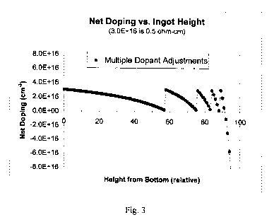
[ 0 0 3 9] Fig. 3 depicts the initial compensation with phosphorus prior to
melting plus multiple
dopant adjustments with boron during growth in which the lower 91% of the
ingot is calculated
to fall within the acceptable range of resistivity;
[ 0 0 4 0] Fig. 4 depicts sampling the melt during growth and for adding
compensating dopant;
[ 0 0 41 ] Fig. 5 depicts, for Example 1, the calculated net doping
concentration for directionally
solidified system (DSS) ingot 060206-2 with initial melt concentrations of 5.1
x 1017 cm 3 for
boron and 5.8 x 1017 cm 3 for phosphorus;
[00421 Fig. 6 illustrates a typical DSS ingot (265 kg), on which the bricks,
wafers, and cell of
Example 1, are positioned;
[00431 Fig. 7 depicts the measured efficiency of cells of Example 1, with
cells ordered
according to their open-circuit voltage values and showing a sharp spike of
five cells at
approximately 13% efficiency, believed to be from p-type wafers with low net
doping cut from
the ingot just before the type flips from p to n (i.e., near the 80% point of
Fig. 5);
[00441 Fig. 8 depicts the measured short-circuit current of cells from Brick
D3 of
Ingot 060206-2 of Example 1, with cells ordered according to their open-
circuit voltage values,
-10-
CA 02680468 2009-09-10
WO 2008/112598 PCT/US2008/056349
showing the spike in short-circuit current for the relatively high efficiency
cells resulting from
the relatively high excess carrier lifetime for low net doping concentration;
[ 0 0 4 5] Fig. 9 depicts the measured open-circuit voltage of cells from
Brick D3 of
Ingot 060206-2 of Example 1, with cells ordered according to their open-
circuit voltage values
(the highest value of open-circuit voltage being 0.623 V, with the five high
efficiency cells
having values ranging from 0.584 V to 0.593 V);
[ 0 0 4 6] Fig. 10 depicts, for Example 2, the calculated net doping
concentration for simulated
feedstock having boron at 0.5 ppmw (6.5 x 1016 cm 3) and an initial
compensation with arsenic
showing the desired p-type net doping below 3 x 1016 cm 3 for 78% of the
ingot;
[ 0 047 ] Fig. 11 is a photograph of silicon Brick B2 from Ingot 060802-1 of
Example 2 with
initial dopant compensation showing 85% of the brick is p-type;
[ 0 0 4 8] Fig. 12 depicts, for Example 2, the efficiency of cells fabricated
from compensated
ingot with Cell # in order from the bottom of the ingot to the top and showing
the drop in
efficiency about Cell #150 corresponding to the transition from p-type to n-
type in the brick;
[ 0 0 4 9] Fig. 13 depicts, for Example 2, the short circuit current density
of cells fabricated from
compensated ingot with Cell # in order from the bottom of the ingot to the top
and showing the
drop in current density about Cell #150 corresponding to the transition from p-
type to n-type in
the brick;
[ 0 0 5 0] Fig. 14 illustrates the sample of silicon melt of Example 3 drawn
into a quartz tube
(left) and a section of silicon removed from tube (right) for measurement from
which the
resistivity and type of the silicon section were determined to provide
information on the net
dopant concentration in the melt;
-11-
CA 02680468 2009-09-10
WO 2008/112598 PCT/US2008/056349
[ 0 0 51 ] Chart 1 is a chart modeling the result of net doping concentration
in the crystal without
gallium dopant addition;
[00521 Chart 2 is a chart modeling the result of net doping concentration in
the crystal with
gallium dopant addition;
[00531 Table 1 is a table showing the measured type, resistivity and lifetime
of the bricks from
Example 2; and
[00541 Table 2 is a table showing the measured type, resistivity and lifetime
of the bricks from
Example 3.
[00551 DETAILED DESCRIPTION OF THE PREFERRED EMBODIMENT
[00561 In accordance with the present invention, the distribution of dopants
within a crystal is
first calculated (if not already known). More specifically, solar cells in
commercial production
often are made from p-type silicon substrates with resistivity varying from
0.5 S2-cm to 5 S2-cm,
corresponding to net acceptor concentrations ranging from 3.04 x 1016 cm 3 to
2.70 x 1015 cm 3
By way of example, a silicon feedstock having a high boron dopant
concentration of
1.14 x 1017 cm 3 may be used to produce a silicon ingot by the directional
solidification process.
Since the segregation coefficient (ratio of concentration in the solid to
concentration in the
liquid) is 0.80 for boron, the doping density of boron in the first silicon to
grow would be
9.12 x 10¹⁶ Cm 3, or three times the desired amount. Because boron accumulates
in the melt
during directional solidification, the boron concentration in the crystal
would become even larger
as the crystal grows. The concentration of boron in the solid silicon would be
calculated by the
Scheil equation (E. Scheil, Z. Metallkd., volume 34, page 70, 1942) which
assumes perfect
stirring in the molten liquid and no diffusion of boron in the solid:
[ 0 0 57 ] Cg(fg) = kC0(1- fg)(k-1) (1)
-12-
CA 02680468 2009-09-10
WO 2008/112598 PCT/US2008/056349
[00581 where Cs is the concentration of boron in the solid silicon, k is the
segregation
coefficient of boron, CO is the concentration of boron in the initial melt,
and fs is the fraction of
the total mass of silicon that has solidified. Fig. 1, which represents
feedstock with an excessive
amount of boron, is a plot of Cs calculated as a function of fs with CO of
1.14 x 1017 cm 3 and k of
0.80. Note that at the beginning of the ingot, Cs is 9.12 x 1016 cm 3 and
increases from that value
to approximately 2.29 x 1017 cm 3 near the end of the ingot. Since the boron
concentration in the
silicon crystal would always be greater than the maximum desired value of 3.04
x 1016 cm 3,
none of this ingot would be suitable for solar cell wafers because the
(calculated) net doping is
too high (> 3.0 x 10¹⁶ CM-3)
[00591 However, as shown in Fig. 2, if phosphorus is added as a compensating
dopant to the
initial melt (i.e., adding phosphorus atoms at a concentration of 1.74 x 10¹⁷
cm 3 to the initial
melt), then the net doping concentration in the crystal (boron concentration -
phosphorus
concentration) can be brought into the desired range over most of the crystal
(specifically,
calculation indicates that the lower 57% of the ingot falls within the
acceptable range of
resistivity). Phosphorus has a segregation coefficient (k) of 0.35, and so
tends to accumulate in
the melt to a greater extent than boron which has a segregation coefficient of
0.80. The result is
that at some point the crystal turns from p-type (positive net doping where
boron dominates) to
n-type (negative net doping where phosphorus dominates), as shown in Fig. 2.
As noted in this
specific example, for the first 57% of the crystal, the net doping density is
within the desired
range of 3.04 x 1016 cm 3 to 2.70 x 1015 cm 3 with the boron concentration
exceeding the
phosphorus concentration. Because both boron and phosphorus are present in the
crystal at a
concentration far below the concentration of silicon atoms (5.0 x 1022 cm 3),
the two types of
impurity atoms are incorporated into the silicon crystal independently
according to their
-13-
CA 02680468 2009-09-10
WO 2008/112598 PCT/US2008/056349
segregation coefficients. That is, boron and phosphorus are assumed to follow
Eq. 1
individually, each without regard to the presence of the other in the melt.
[ 0 0 6 0] In practice, the dopant concentration(s) in the starting silicon
feedstock may be
determined by an analytical technique, such as glow discharge mass
spectroscopy (GDMS) or
inductively coupled plasma mass spectroscopy (ICPMS), and a suitable amount of
dopant to be
added to the starting charge may be calculated so as to make the majority of
the crystal suitable
for solar cell substrates. Usually the dopant would be added in the form of
very low resistivity
(0.002 - 0.005 92-cm) silicon pieces. This method for achieving the desired
net doping
concentration may be termed "Initial Compensation Only", since a single
adjustment to the
doping in the feedstock would be made in the starting silicon charge prior to
melting the silicon
and no adjustment would be made during crystal growth. This would suggest an
accurate assay
of the silicon feedstock (e.g., by GDMS or ICPMS) so that the amount of dopant
present in the
feedstock would be known and the required amount of compensating dopant could
be calculated
to bring most of the silicon crystal into an acceptable range. Although
applicable to any number
of dopants in the silicon feedstock, boron, gallium and phosphorous dopants
are preferred since
they are available in significant quantity. It is noted that this approach is
simple in that the
growth hardware and the growth process for directional solidification need not
necessarily be
changed. However, it does suggest that the assay of the silicon feedstock be
representative of the
whole charge, and also be sufficiently accurate and precise to allow a
calculation of the amount
of dopant to be added in the initial compensation.
[ 0 0 61 ] Assuming the primary dopants are boron and phosphorous, to
summarize the
proportion of the p-type silicon in the melt (See Graph 1):
[ 0 0 621 Condition: [Plppma,s =[Blppma,s (p-n junction)
-14-
CA 02680468 2009-09-10
WO 2008/112598 PCT/US2008/056349
[0063] IPIppmw _ 30.974x 0.80=(1- fs)0.80-i
[B]ppmw 10.811 0.35 = (1- fs)0.35-1
[0064]
Quantity ofp-type [P]/[B] ratio
(% of the ingot) ( mw/ mw)
0 6.55
80 3.17
90 2.32
95 1.70
99 0.82
[ 0 0 6 5] The dopant concentrations in usable compensated of p-type silicon
may be
summarized as follows:
[ 0 0 6 6] Resistivity criteria : 0.5 0=cm to 3 0=cm
[ 0 0 671 NCC (Net current carrier)
[ 0 0 6 81 NCC = [B1ppma,s - [r lppma,s
[ 0 0 6 9] To obtain 0.5 0=cm min., NCC <_ 3.3 x 10¹⁶ a l cm3
[ 0 07 0] To obtain 3 0=cm max., NCC >_ 4.6 x 10¹⁵ a l cm 3
16 a 1cm3 28.0855g
NCC _ 3.3 x 10 3 23 = 1000000 = 0.66ppma
[0071] cm 2.33g 6.02x10 a
15 a 1Cm3 28.0855g
[0072] NCC _ 4.6x10 3 = 23 =1000000=0.09ppma
cm 2.33g 6.02 x 10 a
[ 0 07 3] 0.09 ppma >_ NCC >_ 0.66 ppma
[ 0 0741 From these calculations, a more preferred range of boron and
phosphorus to make solar
cells is:
a. ppmw < Boron (ppmw) < 1 ppmw
b. ppmw < Phosphorus (ppmw) < 2.5 ppmw
-15-
CA 02680468 2009-09-10
WO 2008/112598 PCT/US2008/056349
[ 0 0 7 5] From the forgoing, as represented in Graph 2, starting with a known
level in boron and
phosphorus, the average chemistry of the melt of silicon may be adjusted by
adding boron or
phosphorus and/or diluting with poly-silicon (silicon at 99.9999999% Si
purity) to get the most
quantity of p-type material having a resistivity of 0.5 to 3 S2=cm in the
ingot.
[00761 Is it noted that the upgraded metallurgical silicon may be diluted at
different ratios with
poly-silicon (i.e. silicon produced by the Siemens process) to be in the best
area of the graph.
This action does not change the phosphorus to boron ratio. This ratio can be
modified by adding
small amounts of phosphorus or boron.
[00771 In accordance with one aspect of the present invention, the quantity of
usable p-type
silicon may be increased by adding another p-type compensating dopant (other
than boron); for
example:
p-type dopant Distribution coefficient Atomic weight
Al 2x10 26.98
Zn 1 x10 65.37
Ga 8x10 69.72
I n 4x10 114.82
[00781 These p-type compensating dopants increase the proportion of usable p-
type silicon
after the multi-crystalline solidification of the ingot. It is noted that
gallium (Ga) and aluminium
(Al), which have a high value of distribution coefficient, have a very good
compensation effect
at the end of the crystallization to compensate for the rapid increase in the
phosphorus
concentration.
[00791 The amount of aluminium (Al) or gallium (Ga) to add to the silicon melt
is preferably:
[ 0 0 8 0] 0 ppmw < Gallium (ppmw) < 250 ppmw
-16-
CA 02680468 2009-09-10
WO 2008/112598 PCT/US2008/056349
[00811 0 ppmw < Aluminum (ppmw) < 100 ppmw
NCC _ [B]ppma s + [Ga]ppma,s - [PJppma,s
[Ga]ppma = [Galppmw x 28.0855 = [Ga]pp,,,w x 0.403
69.723
kGa = 0.008
[Galppma,s = 0.008. [Ga]ppma,o ' (1- .fs )0.008-1
[00821 It is further noted that producers of solar cells would prefer to keep
the addition of
boron to a minimum level due to a phenomenon called "light induced
degradation" (i.e., the
initial rapid light-induced degradation of cell performance). As reflected in
Graph 3 compared
with Graph 1, the use of gallium, which has a better stability than boron, as
the compensating
dopant of a silicon feedstock having a high phosphorus to boron ratio, would
be preferred over
boron, to increase the proportion of usable ingot in the production of solar
cells.
[00831 In accordance with another aspect of the present invention,
compensating dopant or
dopants may be added into the crystal growth period itself to substantially
increase the fraction
of the ingot which has net doping in the desired range. More specifically, as
shown in Fig. 3, if
four additional dopant adjustments are made during solidification, the
fraction of crystal that
would suitable for solar cell wafers may be increased from 57% associated with
initial
compensation only to 91 % with initial compensation plus compensation during
growth.
Preferably, the amount of dopant that must be added in a typical production-
scale directional
solidification is initially calculated.
[00841 For example, taking a starting charge of 265 kg of silicon feedstock
doped with boron
to 1.14 x 1017 cm 3, the initial compensation (prior to melting) may be
calculated to require
4.2 kg of silicon doped to 0.005 S2-cm with phosphorus. Following the initial
compensation,
-17-
CA 02680468 2009-09-10
WO 2008/112598 PCT/US2008/056349
silicon doped with boron to 0.004 S2-cm may be added in the following amounts
during growth:
160 g after 58% of the silicon is solidified, 92 g after 76% is solidified, 64
g after 84% solidified,
and 54 g after 89% solidified, resulting in 91% of the ingot being usable.
[ 0 0 8 5] Although calculations such as the above may be made to determine
the required
additions of dopant to maintain the resistivity and type of the crystal in the
desired range, a
preferred approach in accordance with the present invention as shown in Fig. 4
is to sample the
melt periodically to assess net doping in the melt, and to make adjustments
accordingly. The
melt may be sampled by drawing some molten silicon into a quartz tube where it
solidifies. This
melt sample may then be withdrawn from the furnace and the net dopant type
assessed, e.g., by a
hot probe type tester. The resistivity of the sample may alternatively be
determined by direct
electrical measurements (four point probe) or by a non-contact method using an
induction coil
pick up. Further alternatively, a mass spectroscopy analysis may be performed
on the withdrawn
sample to assess the quantity of different dopant species in the melt.
[ 0 0 8 6] After sampling, the required compensating dopant may then added
through a second
port in the furnace as growth continues. This sampling and dopant addition
preferably occurs
without compromising the growth ambient which is usually an inert atmosphere
(e.g., argon)
under reduced pressure (below atmospheric). For example, the required
isolation between the
growth chamber and the melt sampling and dopant addition ports on the furnace
may be
achieved with a load-lock system.
[00871 It is noted that during the sampling, the height of the column of
liquid silicon that is
drawn up into the quartz tube may be controlled by the pressure difference
between the furnace
ambient and the interior of the quartz tube. For example, if the furnace
ambient is maintained at
100 mbar and the interior of the quartz tube is evacuated with a vacuum pump,
this pressure
-18-
CA 02680468 2009-09-10
WO 2008/112598 PCT/US2008/056349
difference of 100 mbar would draw silicon in the quartz tube to a height of
approximately 44 cm.
The solidification of the silicon in the tube is preferably controlled so that
the silicon at the top of
the column solidifies first. Because of segregation of dopants in the silicon,
this first-to-solidify
in the sample column of silicon would mimic the dopant concentration in the
large crystal. Thus,
by measuring the resistivity and type of the topmost silicon in the sampling
tube, the resistivity
and type of silicon that is simultaneously freezing in the crystal may be
determined. However, if
it is desired to maintain the pressure of the ambient in the furnace at some
relatively high value
(e.g., 600 mbar), then the pressure in the sampling tube may be controlled to
draw only a desired
and manageable amount of silicon into the tube. For example, with an ambient
pressure of
600 mbar, reducing the pressure in the tube to 500 mbar will also draw 44 cm
of liquid silicon
into the tube for analysis. In each of these techniques, a silicon sample may
be obtained at any
point during crystal solidification to represent the crystal at that time.
Then, adjustments to the
doping of the melt may accordingly be made in real time to maintain the net
doping in the
solidifying crystal within a desired range.
[00881 The mobility of the majority carriers may be measured (e.g., by the
Hall effect) on the
sample drawn from the melt. Mobility ( ) depends on the total dopant
concentration and
therefore it may be used as an indicator of that concentration over the range
1015 cm 3 to 1019 cm
3. Resistivity (p) depends on the concentration of majority carriers and the
majority carrier
mobility. For example, the resistivity (p) of a p-type sample is given as:
[00891 P=(q pp)-1 (2)
[ 0 0 9 0] where p is the concentration of holes, p is the hole mobility, and
q is the charge on the
electron. A measurement of both p and p may be used to determine p, the net
doping
concentration from Eq. 2. The total doping concentration may be determined
from p. With a
-19-
CA 02680468 2009-09-10
WO 2008/112598 PCT/US2008/056349
knowledge of both total doping and net doping, the amount and type of dopant
to be added to the
melt to maintain net doping within a desired range may be calculated with some
confidence,
particularly if the dopant species are known (e.g., boron and phosphorus). It
should be pointed
out that determination of type and resistivity of the melt sample is adequate
for making
adjustments to the melt, but that the additional determination of majority
carrier mobility enables
more refined control since the net doping of Eq. 2 can then be determined more
precisely.
[ 0 0 91 ] In accordance with the present invention, continuous or semi-
continuous feeding of the
melt with compensating dopant may be employed, rather than the discrete
additions of dopant as
indicated in Fig. 3. If the dopant content (species and concentration) of the
initial silicon charge
is known fairly accurately and precisely, then the delivery of compensating
dopant in a
semi-continuous fashion may be calculated to narrow the range of the net
doping. Of course,
sampling the melt to confirm proper dopant content during such semi-continuous
dopant
compensation mode may still be conducted.
[ 0 0 921 Examples For Implementing The Invention
[ 0 0 9 3] Example 1
[ 0 0 9 4] A candidate silicon feedstock, identified as "Brand A-6N," was
procured. A GDMS
analysis indicated a very high concentration of boron and phosphorus, with
boron at 4.6 ppmw
(12.0 ppma or 6.0 x 1017 cm 3) and phosphorus at 15 ppmw (13.6 ppma or 6.8 x
1017 cm 3). Note
that the boron concentration in the feedstock is 20 times the maximum value
desired in the
silicon crystal (3.0 x 1016 cm 3). Troublesome metals were generally below
their respective
GDMS detection limits, with V below 0.005 ppmw, Li, Ti, Mn, Co, Ni, Ag, and W
all below
0.01 ppmw, S, Cu, Zn, Ga, As, Mo, Sb, and Pb all below 0.05 ppmw, and Cr below
0.1 ppmw.
Only Fe and Al were detected at 0.06 ppmw and at 0.32 ppmw, respectively. A
full-sized ingot
-20-
CA 02680468 2009-09-10
WO 2008/112598 PCT/US2008/056349
(ID 060206-2), with a mass of 265 kg, was produced at Solar Power Industries
in a DSS
(directional solidification of silicon) furnace using 225 kg of the Brand A-6N
feedstock and
40 kg of undoped silicon. Fig. 5 depicts the expected net doping in the ingot
that was calculated
using Eq. 1. The presence of boron and phosphorus in the feedstock was taken
into
consideration, along with the dilution of this feedstock with undoped silicon.
Note that at the
beginning of the ingot the net doping is more than six times the desired
maximum of
3.0 x 1016 cm 3 and only in a small region around the cross-over point near
80% solidification are
wafers expected to be p-type with resistivity less than 0.5 S2-cm, as desired.
As shown in Fig. 6,
bricks were cut from the ingot, wafers were cut from the bricks, and cells
(156 mm square,
270 m thick) were made from the wafers.
[ 0 0 9 5] Wafers cut from Brick D3 of Ingot 060206-2 were processed into 156
mm square cells
in Lot 060214-11. Efficiency values for the 265 cells produced from such brick
are shown in
Fig. 7, as measured under standard test conditions (1 kW/m2, AM1.5, 25 C).
During the
processing of these wafers and the measurement of the completed cells, no
special effort was
made to keep the wafers in the order that they were cut from the brick.
Instead, for purposes of
analysis, the cells were ordered according to their open-circuit voltage (V ,)
value, with cell 1
having the highest V , value and ce11275 having the lowest. Since V , normally
decreases with
decreasing net doping, this ordering would be expected to approximately
reproduce the order of
the wafers in the brick, beginning with cell 1 from the bottom of the brick.
[00961 A noticeable feature of Fig. 7 is the cluster of five cells near cell
number 250 having
efficiency about 13%, significantly greater than the efficiency of other cells
in the lot. These five
cells are believed to be those having wafer resistivity in the range of 0.5 S2-
cm to 5 S2-cm (net
doping from 3.04 x 1016 cm 3 to 2.70 x 1015 cm 3)(i.e., wafers having a high
boron concentration
-21 -
CA 02680468 2009-09-10
WO 2008/112598 PCT/US2008/056349
nearly compensated with phosphorus). As shown in Fig. 8, this is further
supported by
examining the short-circuit current of cells from Lot 060214-11. Again, near
ce11250 there is a
significant increase in the short-circuit current values for the high
efficiency cells. As shown in
Fig. 8, since short-circuit current is most strongly related to excess carrier
lifetime, the lifetime in
the nearly compensated wafers would be considerably higher than lifetime in
wafers with larger
net doping concentration. In fact, it is this larger value of short-circuit
current that allows the
cells to reach a high efficiency level of 13%. The five high efficiency cells
have open-circuit
voltage values ranging from 0.584 V to 0.593 V, also consistent with wafer
resistivity in the
desired range. As shown in Fig. 9, the most efficient cell had an efficiency
of 13.1%, with Js, of
29.6 mA/cm2, Vo, of 0.591 V, and FF of 0.748.
[00971 The benefits observed in Ingot 060206-2 of this Example 1 indicate the
value of
controlled dopant compensation. Even with the very high concentrations of
boron and
phosphorus in feedstock Brand A-6N, some 13% cells were obtained. With
controlled dopant
compensation, done either initially before melting or with multiple dopant
adjustments during
growth, market-worthy cells may be produced in spite of a very high
concentration of dopants in
the silicon feedstock. Similar results were also obtained for cells from Brick
D2 of Ingot
060206-2, thereby indicating that the effects which were observed and
described above are
reproducible.
[0098] Example 2
[ 0 0 9 9] In order to demonstrate the benefits of dopant compensation in a
controlled manner, a
full-sized (265 kg) silicon ingot was produced using intrinsic silicon with
boron added at a
concentration of 0.5 ppmw (6.5 x 10¹⁶ B/cm) . This represented silicon
feedstock which had a
residual boron content at a level which may be obtained by some low-cost
purification processes.
-22-
CA 02680468 2009-09-10
WO 2008/112598 PCT/US2008/056349
With a segregation coefficient of 0.80, the expected boron concentration at
the beginning
(bottom) of a directionally-solidified ingot is 5.2 x 10¹⁶ B/cm3. This is
almost twice the
maximum level of 3.0 x 10¹⁶ B/cm3 desired in a substrate for solar cells, and
which would
increase as the crystal grows as the melt becomes more highly concentrated in
boron. To bring
the net doping concentration into the desired range for this simulated impure
feedstock, the
excess boron was compensated with arsenic in the initial silicon charge. The
purpose was to
demonstrate that feedstock that has a higher-than-desired dopant impurity
concentration may be
compensated into a desired doping range and that solar cells of good
efficiency may be made in
spite of the compensating dopants.
[ 0 010 0] Analysis based on Eq. 1 indicated that arsenic at a concentration
of
8.0 x 10¹⁶ As/cm3 should be added to the initial charge in order to create an
ingot which is p-type
with net doping below 3.0 x 1016 cm 3 over as much of the ingot as possible.
The results of the
analysis are given in Fig. 10 which shows the concentration of boron and
arsenic in the ingot as a
function of ingot height, along with the net doping concentration. Note that
with the addition of
arsenic the brick goes from being unacceptable over its entire height because
of the high
concentration of boron to being acceptable over 78% of its height.
[001011 Ingot 060802-1 of Example 2 was grown by directional solidification
under the
conditions given above. Sixteen bricks were cut from the ingot, each nominally
156 mm x 156 mm x 240 mm. Fig. 11 is a photograph of Brick B2. A clear
demarcation
between the lower p-type section of the brick and the upper n-type section was
indicated by
hot-probe type testing. Specifically, 85% of the height of the brick (206
mm/243 mm) was
p-type, in approximate agreement with the 78% expected from the calculation.
The resistivity
- 23 -
CA 02680468 2009-09-10
WO 2008/112598 PCT/US2008/056349
was measured on the face of the brick and ranged from approximately 0.7 S2-cm
at the bottom to
approximately 8 S2-cm at the end of the p-type region.
[ 0 010 2] Wafers were cut from Brick B2 with a nominal thickness of 240 m.
Type and
resistivity were measured for the wafers after saw damage was removed by a KOH
etch. Excess
carrier lifetime was measured by the quasi-steady state photoconductivity
decay (QSSPCD)
technique after the wafer surfaces were passivated by a phosphorus diffusion
having a sheet
resistance of approximately 40 S2/0 to give an n+pn+ or an n+nn+ structure.
Results are given in
Table 1 for wafers from the bottom of the brick to the top.
[ 0 010 3] Note in Table 1 that the measured wafer resistivities are
consistent with the
calculated net doping curve of Fig. 10. Note also that the measured lifetimes
tend to increase
with resistivity and that lifetimes for the n-type wafers are typically
greater than those for p-type
wafers.
[ 0 010 4] Solar cells, 156 mm square, were fabricated from the wafers cut
from Brick B2 in
cell processing lot 060809-9. The measured efficiencies of cells from the
bottom of the brick to
the top are depicted in Fig. 12. Over the p-type section of the brick, the
cell efficiency was
nearly constant at approximately 14%. Since the solar cell process are
designed for p-type
wafers, the cell efficiency falls off dramatically for the n-type wafers in
the upper section of the
brick. Over the p-type section, cells had a median efficiency of 13.5%, with
short-circuit current
of 7.22 A, open-circuit voltage of 0.604 V, and fill factor of 0.754. These
parameter values are
all respectable for production multicrystalline solar cells. The highest
efficiency was 14.1%,
with short-circuit current of 7.21 A, open-circuit voltage of 0.613 V, and
fill factor of 0.776. A
plot of short circuit current density for these compensated cells is depicted
in Fig. 13. Note the
correlation of this current density with measured lifetime for cells made from
p-type wafers. The
-24-
CA 02680468 2009-09-10
WO 2008/112598 PCT/US2008/056349
reduced efficiency and short circuit current observed for cells from near the
bottom of the ingot
(approximately the first 15 cells) was likely associated with impurities
coming from the crucible
material itself (fused silica) or from the crucible coating (silicon nitride).
(The crucible holds the
molten silicon.) The slight increase in short circuit current density for
cells near the end of the
p-type region (near cell 160) is believed to be associated with the relatively
high resistivity of
those wafers.
[ 0 010 5] For comparison, cells were also made from wafers cut from Ingot
060501-1 which had
the same quality of intrinsic silicon as Ingot 060802-1, but doped only with
boron to a resistivity of
approximately 2 S2-cm with no compensating n-type dopant. These cells had a
median efficiency of
13.8%, with short-circuit current of 7.52 A, open-circuit voltage of 0.598 V,
and fill factor of 0.746. The
highest efficiency was 14.5%. Note that cells from the compensated ingot had
median efficiency
0.3% (absolute) lower than the median efficiency for cells from the
uncompensated ingot. This difference
was consistent with the efficiency penalty for compensated silicon associated
with reduced minority
carrier diffusion constant described earlier.
[ 0 010 6] Example 3:
[ 0 010 7] In order to demonstrate the benefits of gallium dopant for N-Type
silicon feedstock, a
full-sized (265 kg) multi-crystalline silicon ingot was produced: 90.60 kg of
N-Type silicon was charged
with 174.40 kg prime semiconductor grade poly silicon raw material. The
initial dopant concentration
included 0.41 ppmw boron (5.74 x 10¹⁶ B/cm3) and 1.15 ppmw phosphorus (5.23 x
1016 P/cm). Since
gallium is a P-Type material, higher N-Type dopant concentration was required
for testing purpose.
Another 1.85 ppmw phosphorus (8.37 x 10¹⁶ P/cm3) in highly-doped wafers (0.002
S2cm) shape was
added to make the fmal charging silicon feedstock with 3.0 ppmw phosphorus
(1.36 x 10¹⁷ P/cm3) of
concentration.
[ 0 010 8] For comparison, Chart 1 shows the net doping concentration from the
bottom to the top
of the ingot (boron concentration - phosphorus concentration) if the silicon
ingot was cast without
- 25 -
CA 02680468 2009-09-10
WO 2008/112598 PCT/US2008/056349
any other dopant addition. The entire ingot would be N-Type which would not be
suitable for a
substrate for solar cells.
[ 0 010 9] Gallium has a segregation coefficient (k) of 0.008, which is very
small compared
to boron (0.8) and phosphorus (0.35), and tends to accumulate in the melt to a
much greater
extent. Therefore, to compensate for this N-Type dopant concentration, 109.25
ppmw (2.20 x
1018 Ga/cm3) of gallium was doped in the form of pure gallium (99.99999%)
pellets shape.
More specifically, as shown in Chart 2, with the addition of gallium, the net
doping
concentration in the crystal (boron concentration + gallium concentration -
phosphorus
concentration) is brought into the desired range over most of the crystal (>
80%). The top 15%
was cropped due to the impurity concentration and low resistivity. The charge
was molten and
cast into a multi-crystalline ingot, 080107-3, in a production DSS
(Directional Solidification
System) furnace.
[001101 The ingot was cut into 16 bricks on the Squarer saw following the
standard ingot
cutting procedure. One center brick, B2, one corner brick, D 1, two side
bricks, B 1 and B4, were
tested for excess carrier lifetime, N/P-Type, and resistivity. The testing was
performed on the
face of the bricks. The resistivity ranged from -0.8 92cm from the bottom to -
0.5 92cm on the top
of the bricks. The entire ingot was P-Type which demonstrated a successful
compensation of
dopant concentration. The detailed results are shown in Table 2 (showing the
measured brick
resistivities being consistent with the calculated net doping curve of Chart
2).
[001111 Two bricks, B2 and D 1, were etched in KOH bath to remove the saw
damage on
the surface. Wafers were cut from two bricks with a nomina1220 m. Solar
cells, 156 mm
square, were fabricated from the wafers using standard solar cell processing
as Lot # 080115-1.
Cells had a median efficiency of 14.55%, with short-circuit current of 7.40 A,
the open-circuit
-26-
CA 02680468 2009-09-10
WO 2008/112598 PCT/US2008/056349
voltage of 0.605 V, and fill factor of 0.791. These parameter values are all
respectable for
production of multi-crystalline solar cells. The highest efficiency is 15.08%,
with short-circuit
current of 7.55 A, the open-circuit voltage of 0.61 V, and fill factor of
0.798.
[001121 Example 4:
-27-
CA 02680468 2009-09-10
WO 2008/112598 PCT/US2008/056349
[001131 Upgraded metallurgical silicon with initial dopant concentration of
1.5 ppmw of
boron and 4.5 ppmw of phosphorus is melted with poly-silicon in a
crystallization furnace. The
ratio of UMG-Si to poly-Si is 1:2. The amount of p-type silicon having a
resistivity in between
0.5 0^ cm and 3 0^ cm is approximately 79.6% of the ingot (an increase of 72%
of ingot usage
over similar example without poly-silicon).
[001141 Example 5:
[001151 Upgraded metallurgical silicon with initial dopant concentration of
0.5 ppmw of
boron and 1.5 ppmw of phosphorus is melted in a crystallization furnace. The
equivalent of
approximately 25 ppmw of gallium is added to the melt and crystallization is
carried out. The
amount of p-type silicon having a resistivity in between 0.5 S2 ^ cm and 3 S2
^ cm is
approximately 96.8% of the ingot (an increase of 17% of ingot usage over
similar example
without gallium).
[001161 Example 6:
[001171 Upgraded metallurgical silicon with initial dopant concentration of
0.5 ppmw of
boron and 2.5 ppmw of phosphorus is melted in a crystallization furnace. The
equivalent of
approximately 65 ppmw of gallium is added to the melt and crystallization is
carried out. The
amount of p-type silicon having a resistivity in between 0.5 S2 ^ cm and 3 S2
^ cm is
approximately 96.1% of the ingot (an increase of 62% of ingot usage over
similar example
without gallium).
[001181 Example 7:
[001191 Upgraded metallurgical silicon with initial dopant concentration of
0.4 ppmw of
boron and 3.0 ppmw of phosphorus is melted in a crystallization furnace. The
equivalent of
approximately 109 ppmw of gallium is added to the melt and crystallization is
carried out. The
- 28 -
CA 02680468 2009-09-10
WO 2008/112598 PCT/US2008/056349
amount of p-type silicon having a resistivity in between 0.5 S2 ^ cm and 3 S2
^ cm is
approximately 91.4% of the ingot, an increase of 91% of ingot usage over
similar example
without gallium).
[ 0 012 0] Example 8:
[001211 Upgraded metallurgical silicon with initial dopant concentration of
0.4 ppmw of
boron and 3.0 ppmw of phosphorus is melted in a crystallization furnace. The
equivalent of
approximately 0.37 ppmw of boron is added to the melt and crystallization is
carried out. The
amount of p-type silicon having a resistivity in between 0.5 S2 ^ cm and 3 S2
^ cm is
approximately 65.0% of the ingot (a decrease of 26% of ingot usage over
Example 7 above).
[ 0 012 2] Example 9:
[ 0 012 3] Dendritic web silicon ribbon crystals were grown in Run SPI-101-5.
The
dendritic web crystal growth technique was different from the directional
solidification technique
employed in the above Examples in that crystals are grown at atmospheric
pressure rather than at
reduced pressure, the melt volume was much smaller at 0.3 kg rather than 265
kg, crystals were
single crystal ribbon that exit the growth chamber rather than a
multicrystalline ingot which
remained inside the growth chamber, and melt volume remained approximately
constant during a
crystal growth run rather than decreasing during the run. It is also noted
that operation at
atmospheric pressure facilitated adding dopant to the melt and also sampling
the melt.
[ 0 012 4] The dendritic web growth run started with a 335 g melt to which 2.3
x 1019 boron
atoms were added via silicon doped with boron to 0.0045 S2-cm. The dendritic
web crystal
grown from this melt was measured to be p-type with a resistivity of 0.18 S2-
cm. This resistivity
was less than the minimum of 0.5 S2-cm desired for solar cell substrates.
Consequently, the melt
was compensated by adding arsenic (n-type dopant) after the melt was
replenished with intrinsic
-29-
CA 02680468 2009-09-10
WO 2008/112598 PCT/US2008/056349
silicon to replace the silicon removed from the melt in the form of the
crystal. A total of
3.8 x 10¹⁹ arsenic atoms were added via silicon doped with arsenic to 0.0028
S2-cm. A dendritic
web crystal grown after this addition of arsenic to compensate the boron was
measured to be
p-type with a resistivity of 6.9 92-cm. Thus, the resistivity was raised above
the minimum level
of 0.5 S2-cm, as desired.
[ 0 012 5] The melt was sampled by inserting a quartz tube into the melt and
drawing some
molten silicon into the tube with the aid of a vacuum pump. The silicon sample
was allowed to
cool and solidify in the quartz tube, and the tube was then withdrawn from the
furnace. The
quartz tube with silicon sample inside is shown in Fig. 14 along with a slug
of silicon that was
removed from the tube for measurement. The silicon slug had a length of 0.962
cm and a
diameter of 0.292 cm. From a hot-probe type tester, it was determined to be n-
type. Also, a
four-point probe measurement was used to measure its resistivity of 0.31 S2-
cm. Consequently,
the slug had a higher concentration of arsenic than boron, as expected for a
melt from which
6.9 S2-cm, p-type crystals were grown, given that the segregation coefficient
for boron is 0.80
and for arsenic is 0.30.
[ 0 012 6] The dendritic web crystal growth of Example 3 demonstrates that the
resistivity
and type of a silicon crystal may be adjusted during a crystal growth run to
an acceptable value
(> 0.5 S2-cm, p-type) by adding compensating dopant to the melt and that the
melt may be
sampled by drawing molten silicon into a quartz tube, then testing the
solidified sample to
determine net dopant type and resistivity.
[ 0 012 7] The present disclosure includes that contained in the appended
claims, as well as
that of the foregoing description. Although this invention has been described
in its preferred
form with a certain degree of particularity, it is understood that the present
disclosure of the
-30-
CA 02680468 2009-09-10
WO 2008/112598 PCT/US2008/056349
preferred form has been made only by way of example and that numerous changes
in the details
of construction and the combination and arrangement of parts may be resorted
to without
departing from the spirit and scope of the invention.
[ 0 012 8] Now that the invention has been described,
[ 0 012 9] WHAT IS CLAIMED IS:
-31-