Note : Les descriptions sont présentées dans la langue officielle dans laquelle elles ont été soumises.
CA 02683617 2009-10-09
WO 2008/125818 PCT/GB2008/001261
FINGERPRINT DETECTION
The invention relates generally, but not exclusively, to an apparatus for and
s method of detecting fingerprints. More specifically, but not exclusively,
the
invention relates to a method of and apparatus for detecting fingerprints by
creating a differential charge density with respect to the surrounding
surface in the region of a deposited fingerprint.
io It is widely known to locate and detect fingerprints deposited on metal or
other surfaces using chemical reactions with either the eccrine (amino acid)
and/or sebaceous (fatty acid) content of a fingerprint residue. Other
methods of detecting latent fingerprints involve using the fingerprint residue
as an insulator against electrochemical or reduction/oxidation (redox)
15 reactions. Such methods are not usually suitable when the surface on which
the fingerprint is deposited has become wetted (removing the aqueous
eccrine content) or damaged (removing the sebaceous content). A surface
can become wetted, or damaged by weathering or cleaning, for example.
2o Another known technique measures the difference in electrical potential
between a metal substrate on which a fingerprint has been deposited and
a metal probe. The technique exploits a discovery made by Lord Kelvin in
the nineteenth century, which is that different metals, connected
electrically, have a potential difference between them determined by the
25 work function of the metals. The work function of a particular metal is a
measure of the ease with which an electron can leave the surface of the
metal. The chemicals found in a fingerprint deposit cause corrosion of a
CA 02683617 2009-10-09
WO 2008/125818 PCT/GB2008/001261
2
metallic surface. The work function of a metal changes where it has been
corroded by a fingerprint. Therefore a work-function based technique
relies on measuring the differences in work function across the whole of a
surface of a metal where it is suspected a fingerprint has been deposited.
Clearly, this can be a time consuming and haphazard process.
It is desirable to be able to locate and identify fingerprints deposited on a
wide variety of surfaces even when such surfaces have been exposed to
outdoor conditions or have been cleaned, for example by persons trying to
io hide their actions. The present invention seeks to avoid or mitigate at
least
one or more of the problems of the prior art by providing an apparatus for
and method of detecting latent fingerprints which is suitable for use on a
wide variety of materials, for example where the fingerprint residue has
been diminished.
According to a first aspect, the invention provides a method of and/or
apparatus for locating and detecting at least part of a fingerprint deposited
on a surface, comprising means for setting up an electric field such that a
differential charge density is produced coincident the location of at least
part
of a fingerprint deposited on the surface; and a detection element, wherein
the detection element is selectively attractable to or repellable from the
surface coincident the differential charge density in the region of the
fingerprint deposit, such that at least part of a fingerprint deposited on the
surface can be located and detected.
Preferably, the electric field is set up such that the charge density of the
surface at the fingerprint deposit is lower than the charge density of the
CA 02683617 2009-10-09
WO 2008/125818 PCT/GB2008/001261
3
surrounding region of the surface. The electric field may be set up such that
there is a potential difference across the surface. The electric field may be
from, say, 0 to 5 KV, say from 0 to 3kV, for example in the order of 2.5kV.
Additionally or alternatively, the detection element may comprise a
conductive powder, for example a black conducting powder, which may be
applied to the surface, for example such that in the area or location of the
deposited fingerprint or part thereof, the conductive powder may be
selectively attracted to or repelled from the deposited fingerprint or part
io thereof, thereby providing a visualisation of the deposited fingerprint or
part
thereof.
The detection element may also comprise ceramic beads coated in a or the
conductive powder, such that in the location of the deposited fingerprint or
part thereof, at least a part of a or the conductive powder may be removed
from the ceramic beads and may be attracted to or repelled from the
fingerprint deposit, thereby providing a visualisation of the deposited
fingerprint or part thereof. The detection element may comprise an aerosol
spray, which may comprise a powder, say a conductive powder which in the
2o area or location of the fingerprint or part thereof, may be attracted to or
repelled from the deposited fingerprint or part thereof, for example thereby
providing a visualisation of the deposited fingerprint or part thereof.
A second aspect of the invention provides apparatus for applying a potential
across an irregularly shaped object, the apparatus comprising a first clamp
means and a support surface, between which the article is retainable, and a
pair of contacts for contacting the article held between the clamp and
CA 02683617 2009-10-09
WO 2008/125818 PCT/GB2008/001261
4
support surface, at least one of the contacts comprising reciprocable
portions to accommodate different portions of said object.
Preferably one or both of the clamp means and the support surface are
reciprocable towards and away from one another. Preferably one or both of
the clamp means and the support surface are rotatable.
At least one of the contacts preferably comprises a spring to provide said
reciprocable portion. Additionally or alternatively, other resilient means may
lo be provided.
Exemplary embodiments of the invention will now be described by way of
example only and with reference to the accompanying drawings in which:
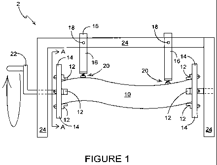
is Figure 1 shows a diagram of an apparatus suitable for detecting at
least part of a latent fingerprint according to one embodiment of the
present invention;
Figure 2 shows a view along line AA of the apparatus of Figure 1;
Figure 3 shows a more detailed diagram of the brass rod and
20 bronze plunger contact arrangement of Figure 1;
Figure 4 shows a more detailed diagram of the clamping mechanism
of Figure 1; and
Figure 5 shows ridge detail development for a fingerprint deposited
on brass, five days after deposition. (a) shows the degree of redox
25 corrosion visible after washing in water, acetone and then water
and (b) shows the same fingerprint after subsequent electrostatic
enhancement.
CA 02683617 2009-10-09
WO 2008/125818 PCT/GB2008/001261
The exemplary method described and depicted herein involves applying an
electrical potential of the order of 2.5kV to a metallic sample upon which a
fingerprint has been deposited. The applied potential difference creates a
5 charge density at the surface of the sample material. At the place where a
fingerprint has been deposited (before it was damaged or wetted), the
charge density is different relative to the charge density of the
surrounding area of the sample surface. This is due to the effect that the
chemicals comprised in the fingerprint deposit have had on the metallic
io sample; that is, a corrosion of the metallic surface. A conducting powder
is
then applied, using at least one of two methods which are described
below, the conductive powder being attracted to and adhering to the
fingerprint.
is Figure 1 shows a diagram of an apparatus 2 for detecting a latent
fingerprint 50 (not shown in Figure 1) on a sample material 10 clamped
within the apparatus 2. The apparatus 2 includes a supporting frame 24,
a pair of circular plates or disks 14 rotatably mounted to opposing portions
of the supporting frame 24, a cranked handle 22 extending from an
2o external surface of one of the circular plates 14 and through the frame 24,
a pair of rods 16 and a high voltage unit (not shown).
Each circular plate 14 includes four clamping mechanisms 12, shown more
clearly in Figures 2 and 4, which are fully adjustable radially inwardly or
25 outwardly across the circular plate 14 until contact is made with the
sample material 10. Each clamping mechanism 12 is adjustably mounted
to the circular plate 14 by a clamping plate 30, which is attached via a nut
CA 02683617 2009-10-09
WO 2008/125818 PCT/GB2008/001261
6
and bolt arrangement 32 to a clamping member 34. The clamping
mechanism 12 is fully adjustable across the circular plate so as to be able
to clamp sample material 10 of varying sizes (not shown) between the
clamps 12.
The circular plates 14 are rotatable about a principal axis of rotation X
using the handle 22 or other suitable mechanism. The clamped sample
material 10 is, in this embodiment, an irregularly shaped brass object
which is believed to have a fingerprint deposited thereon by an unknown
io person.
The rods 16 are made of brass in this embodiment, although any suitable
conductive material may be used. As shown more clearly in Figure 3,
each rod 16 includes a plunger contact 20 which is mounted to an end of
the rod 16 by a spring 21 in this embodiment, although any suitable
resilient biasing means could be used. The rods 16 are adjustably
mounted to the frame 24, say by grub screws 18, such that they extend
inwardly of the apparatus 2 toward the sample material 10 in use. This
arrangement enables the rods 16 to be adjusted to ensure that the
plunger contact 20 is in contact, in use, with the sample material 10. The
spring 21 enables the plunger contact 20 to adjust to and follow the
contours of irregularly shaped surfaces of a sample material 10 whilst it is
rotated.
Electric potential is provided, in use, by the high voltage unit (not shown),
based around a Brandenburg 3590 series high voltage module. The unit
enables the generation of a continuously variable potential from 0-2.5kV.
CA 02683617 2009-10-09
WO 2008/125818 PCT/GB2008/001261
7
Other high voltage modules may be used which generate different
potentials.
An electrical potential of the order of 2.5kV is applied through the
s conductive brass rods 16. It has been observed that the higher the
voltage the better the observed affect and therefore many voltages other
than 2.5kV will create a differential charge density sufficient to enable a
latent fingerprint to be detected and identified. It should be clear to a
person skilled in the art that the present invention is not limited solely to
io the application of a potential voltage of 2.5kV and that lower or higher
potentials may be applied.
It will also be clear to a person skilled in the art that any suitable means
of
clamping the sample material securely so that it can be rotated or tilted
15 when being examined can be used and that the present invention is not
limited to only the mechanical arrangement of clamps and plates as
described with reference to Figures 1 through 4. For example two, three
or more clamps 12 and/or other types of clamps (not shown) can be used.
zo The apparatus 2 may also be used to enhance fingerprints on non-metallic
(i.e. insulating) sample materials 10. Non-metallic objects are clamped or
clampable in the same way as described with reference to Figures 1
through 4 above, although the rods 16 and plunger contacts 20 are
removed. An electric field is then applied in the vicinity of the non-
25 metallic sample material 10 by means of two metal, for example brass,
plates (not shown) positioned on either side of the sample material 10 and
CA 02683617 2009-10-09
WO 2008/125818 PCT/GB2008/001261
8
charged with a potential of opposing polarities. It should be noted that if
the substrate containing the residue also polarizes, then the differential
charge density set up may not distinguish as well between the fingerprint
trace where the fingerprint residue reacted with the sample and the
s surrounding area. Nevertheless, fingerprint traces may still be resolved.
When a latent fingerprint needs to be located and detected on the surface
of a sample material 10, using the apparatus as described above, at least
two methods may be used to apply a conducting powder.
The first method requires the introduction to the sample material 10 of
ceramic spherical beads, for example of approximately 10 microns in
diameter, which are coated in a fine granular (N2 micron) black
conducting powder. The ceramic spherical beads are then rolled over the
1s surface of the sample material 10 (aided by the turning thereof). The
coated ceramic spherical beads are known in the art and are commercially
available.
The ceramic spherical beads act as a carrier for the conducting powder
onto the sample material 10. The beads do not themselves adhere to the
sample material 10, the conducting powder on them does. The ceramic
beads are spherical so they can easily move across the surface of the
sample material 10.
2s The conducting powder is charged when the ceramic spherical beads come
into contact with the charged sample material 10. The beads roll across
CA 02683617 2009-10-09
WO 2008/125818 PCT/GB2008/001261
9
the surface of the sample material 10 and the conducting powder acquires
the potential of the sample material 10. When fingerprint residue is
reached, these areas have a potential difference relative to the
surrounding area and the conducting powder is attracted to or repelled
from this area due to electrostatic effects.
On a metallic sample material 10, the grains attract a charge equal to the
charge of the metallic sample material 10. On contact with a latent
fingerprint, the lower potential of the fingerprint residue/metal corrosion
io attracts the grains from the beads and onto that part of the metal
coincident the fingerprint residue/corrosion.
In Figure 5 a brass sample surface is illustrated onto which a fingerprint
has been deposited. The sample surface has been washed in water,
acetone and then water again. The image of Figure 5 (a) has been taken
five days after deposition of the latent print and Figure 5 (b) shows the
ridge detail development of the same fingerprint after subsequent
electrostatic enhancement using the method and apparatus of the present
invention. It is shown that after using electrostatic enhancement, the
fingerprint can be detected and identified whereas before, the fingerprint
could not be seen.
After electrostatic treatment, the conducting powder is generally
vulnerable to disturbance after the electric charge has been removed. By
heating the sample material 10 after treatment to a temperature of, for
example 150 C, the powder will bind to the sample material 10, thereby
producing a more durable sample.
CA 02683617 2009-10-09
WO 2008/125818 PCT/GB2008/001261
On a non-metallic sample material 10 , the applied electric field will
polarize components within the fingerprint residue encouraging
(uncharged) grains to be attracted to (or repelled from) the charge on the
5 residue.
The second method usually involves the spraying of fine granular
conducting powder onto the sample material 10 by means of say an
aerosol. The aerosol nozzle is charged with a potential of opposite polarity
lo to the sample material 10. On the metallic sample material 10, the
charged conducting powder would be attracted to the lower potential on
the sample material 10 either co-incident with the fingerprint
residue/corrosion or the surrounding area such that either an inverted or
normal trace of the fingerprint is obtained.
On a non-metallic sample material 10, the charged conducting powder is
attracted to the polarized charge on the residue of opposite polarity to the
charge on the powder.
It will be appreciated that the method and apparatus of the invention
allows investigation of a substrate to determine whether or not a
fingerprint or part thereof is present. The method is rapid insofar as the
whole of the substrate need not be examined in minute detail, for example
by setting up an examination array comprising a plurality of points for
investigation.
Whilst the inventors do not wish to be limited by any theory, the
CA 02683617 2009-10-09
WO 2008/125818 PCT/GB2008/001261
11
mechanism for this process, when used on metallic materials, is thought
to be a consequence of the corrosion on the metal surface that leads to
both impurities and lattice imperfections, which will have the affect of
locally increasing the resistivity of the metal at the site of the corrosion.
If
s a potential is applied to the metal sample 10 then, under electrostatic
conditions, the charge will move entirely to the outer surface with the
electric field inside the metal being zero. Areas of corrosion with increased
resistivity will behave more like a dielectric and the charge density in
these areas (cr') will be less than the charge density at other parts of the
lo surface (Q). Using Gauss' Theorem, both the electric field and potential at
a given point above the disk will be less above a corroded area.
More specifically, in a section through a metal disk under electrostatic
equilibrium, where a represents a Gaussian surface drawn partly through
15 the surface of the metal that has a surface area in the plane parallel to
the
exterior surface of the metal of A, the Gaussian surface contains a charge
q = Q.A.
From Gauss' law,
20 q = co f E.dA
where co = permitivity of free space and, at all points on the Gaussian
surface E and dA have the same direction.
Assuming that E has the same magnitude at all points on the Gaussian
25 surface then
q=EOEf dA=EoE.A
CA 02683617 2009-10-09
WO 2008/125818 PCT/GB2008/001261
12
and therefore
E = q/ coA
By the same derivation, if the Gaussian surface a" (taken or drawn
through a corroded area) has the same surface area A then
q' =Eo E'f dA = Eo E'.A
and therefore
E' = q'/EoA
io As q' < q then it follows that E' < E.
Further, as the potential difference (Av) between two points separated by
a distance d is given by
d
6,V= fE.dS
0
the potential at a given point above Gaussian surface a' will be less than
the potential above a.
It will be appreciated by those skilled in the art that various changes may
be made without departing from the scope of the present invention, for
2o example, the size and shape of the frame and clamping arms and
clamping mechanism may be adjusted to accommodate sample materials
of differing size or shape. It is also envisaged that other methods of
applying the conducting powder would work equally well and would still
produce the desired effect.
CA 02683617 2009-10-09
WO 2008/125818 PCT/GB2008/001261
13
Also, the ceramic beads need not be used. For example a conducting
powder may be applied by other means, such as dusting.
It will also be understood by the skilled addressee that a detection
element may be configured to be attracted to the area where the
fingerprint is not or to be repelled from the area where the fingerprint, or
part thereof, is deposited.
The conducting powder may be any size, for example 10 microns. The
io metallic material may be for example, copper, steel, aluminium, brass (as
described above) or any other suitable metallic material.
The circular plates 14 may also be movable toward and away from one
another to accommodate different sized and shaped articles.
The method need not be practiced on an article isolated from its
environment. In particular, the method may be practiced on an article in
situ. For example, a potential and the detection element may applied
directly to the article in situ.