Note : Les descriptions sont présentées dans la langue officielle dans laquelle elles ont été soumises.
CA 02687696 2015-02-19
DYNAMIC VOLTAGE SAG CORRECTION
CROSS-REFERENCE TO RELATED APPLICATIONS
[0001] This application clairi,s priority from U.S. Provisional
Application No.
60/917,441 , filed May 11 , 2007, U.S. Provisional Application No. 60/938,054,
filed May
15, 2007, and U.S. Application No. 11/835,000, filed August 7, 2007.
FIELD
[0002] The subject of the disclosure relates generally to dynamic voltage
sag
correction. More specifically, the disclosure relates a device and method for
optimal
utilization of the kVA capability of a dynamic voltage sag correction device
which can be
adapted for use with a plurality of input voltages.
BACKGROUND
[0003] An electrical load which receives power through an AC power system
is
generally designed to operate reliably when the actual supply input voltage is
within
approximately 10% of the rated supply input voltage. A voltage sag (or dip)
can refer to a
temporary reduction of the rms AC voltage in which the actual supply input
voltage is
below approximately 90% of the rated supply input voltage. A dynamic voltage
sag
correction device can refer to a device which is capable of correcting
temporary voltage
sags in a voltage input signal that is being provided to a load. Voltage sags
can be caused
by startup of a large load within a facility, a circuit fault, a problem at a
utility company, a
problem with a generator, or any of a number of other reasons. The dynamic
voltage sag
correction device is generally inserted between the voltage input and the
load, and includes
a combination of circuit elements and logic which are adapted to provide a
correction
signal almost instantaneously.
1
CA 02687696 2009-11-09
WO 2008/141092 PCT/US2008/063067
[0004] Traditional dynamic voltage sag correction devices are
packaged according to their current and voltage ratings. For example, a first
dynamic voltage sag correction device for a three-phase input voltage may be
rated
for 100 amps (A) at 277 volts (V), and have a corresponding kilovolt ampere
(kVA)
rating of ((277 V)* (100 A)* (V3)) / 1000 = 48.0 kVA. A second dynamic voltage
sag correction device for a three-phase input voltage may be rated for 100 A
at 120
V such that its kVA rating is 20.8 kVA. Because components in a dynamic
voltage
sag correction device are selected primarily according to the current rating,
the first
and second dynamic voltage sag correction devices are similar in physical
size,
components used, and cost. In other words, the second dynamic voltage sag
correction device with a kVA rating of 20.8 kVA costs almost as much as the
first
dynamic voltage sag correction device with a kVA rating of 48.0 kVA.
Traditional
manufacturers generally make a distinct dynamic voltage sag device for each
distinct input voltage.
[0005] Manufacturing a distinct dynamic voltage sag correction device
for each distinct input voltage also increases the cost of manufacturing. For
example, a first dynamic voltage sag correction device with a 208 V rating may
be
manufactured for use only with a 208 V input, a second dynamic voltage sag
correction device with a 240 V rating may be manufactured for use only with a
240
V input, and so on. Each of these differently rated dynamic voltage sag
correction
devices require different parts and are manufactured and packaged separately.
As
a result, dynamic voltage sag correction device manufacturers are required to
purchase and inventory parts for a plurality of different devices.
Manufacturing
costs would be reduced if a single dynamic voltage sag correction device could
be
adapted for use with a plurality of input voltages.
[0006] In some instances, dynamic voltage sag correction devices are
used at a fraction of their ratings. For example, a dynamic voltage sag
correction
device with a three-phase voltage rating of 480 V (in a 277 V line-to-neutral
system)
may be used in a system which is supplied by an input voltage of 208 V (in a
120 V
line-to-neutral system). As a result, the kVA throughput of the dynamic
voltage sag
- 2 -
CA 02687696 2009-11-09
WO 2008/141092 PCT/US2008/063067
correction device is reduced below its rating. Traditional dynamic voltage sag
correction devices are further limited in their ability to accept higher input
voltages
such as a 600 V line-to-line signal. To handle these high voltages,
specialized
heavy duty devices are manufactured. The specialized devices are manufactured
and packaged separately from lower voltage dynamic voltage sag correction
devices, resulting in additional costs and the need to inventory additional
parts.
[0007] Thus, there is a need for a dynamic voltage sag correction
device in which optimal utilization of the kVA capability of the device can be
achieved regardless of the input voltage. Further, there is a need for a
dynamic
voltage sag correction device which can be configured for use with a plurality
of
distinct input voltages. Further, there is a need for a high voltage dynamic
voltage
sag correction device which is able to provide a correction signal in an even
higher
voltage system.
SUMMARY
[0008] An exemplary dynamic voltage sag correction device includes
an input terminal adapted to receive a first operating signal, where the first
operating signal has a line-to-neutral voltage. The first operating signal is
provided
to a load through an output terminal which is in electrical communication with
the
input terminal. The dynamic voltage sag correction device also includes a
regulator
module including a rectifying device, a storage unit, and an inverter
switching
device. The rectifying device is adapted to rectify a line-to-line input
signal, where
the line-to-line input signal is obtained from a second operating signal
having the
line-to-neutral voltage and a third operating signal having the line-to-
neutral
voltage. The storage unit is adapted to store energy corresponding to the
rectified
line-to-line input signal, and the inverter switching device is adapted to use
the
stored energy to generate a correction signal during a voltage sag. An
injection
transformer in electrical communication with the regulator module is adapted
to
reduce a voltage of the correction signal. A bypass switch is in electrical
communication with the input terminal and the output terminal. The bypass
switch
- 3 -
CA 02687696 2009-11-09
WO 2008/141092 PCT/US2008/063067
is in a closed position during a normal operating condition such that the
injection
transformer is bypassed, and in an open position during at least a portion of
the
voltage sag such that the injection transformer is energized.
[0009] An exemplary method of correcting a voltage sag condition
includes connecting a load to an output terminal such that the load receives a
line-
to-neutral voltage of a first operating signal through the output terminal. A
line-to-
line input signal is rectified, where the line-to-line input signal is
obtained from a
second operating signal having the line-to-neutral voltage and a third
operating
signal having the line-to-neutral voltage. Energy corresponding to the
rectified line-
to-line input signal is stored in a storage unit. A voltage sag is detected,
and an
inverter switching device is used to generate a correction signal with the
stored
energy in response to the detected voltage sag. A static bypass switch is
opened
such that an injection transformer is not bypassed. The injection transformer
is
used to reduce a voltage of the correction signal such that the correction
signal can
be provided to the load.
[0010] Another exemplary dynamic voltage sag correction device
includes an input terminal and an output terminal in electrical communication
with
the input terminal. The output terminal is capable of providing a first
operating
signal to a load, where the first operating signal has a line-to-neutral
voltage. An
input boost transformer is adapted to increase a line-to-line voltage obtained
across
a second operating signal having the line-to-neutral voltage and a third
operating
signal having the line-to-neutral voltage such that an increased line-to-line
input
signal is provided to a regulator module. The regulator module is connected
between the input terminal and the output terminal and includes a rectifying
device,
a storage unit, and an inverter switching device. The rectifying device is
adapted to
rectify the increased line-to-line input signal, and the storage unit is
adapted to store
energy corresponding to the rectified increased line-to-line input signal. The
inverter switching device is adapted to use the stored energy to generate a
correction signal during a voltage sag. An injection transformer is in
electrical
communication with the regulator module and is adapted to reduce a voltage of
the
- 4 -
CA 02687696 2009-11-09
WO 2008/141092 PCT/US2008/063067
correction signal. A secondary winding of the injection transformer is
connected in
series between the input terminal and the output terminal. A bypass switch is
in
electrical communication with the input terminal and the output terminal. The
bypass switch is in a closed position during a normal operating condition such
that
the injection transformer is bypassed, and in an open position during at least
a
portion of the voltage sag such that the injection transformer is energized.
[0011] Another exemplary method of correcting a voltage sag
condition includes connecting a load to an output terminal such that the load
receives a line-to-neutral voltage of a first operating signal. An input boost
transformer is used to increase a line-to-line voltage obtained across a
second
operating signal having the line-to-neutral voltage and a third operating
signal
having the line-to-neutral voltage such that an increased line-to-line input
signal is
provided to a regulator module. The increased line-to-line voltage is
approximately
equal to a voltage rating of a regulator module. The increased line-to-line
input
signal is rectified, and energy corresponding to the rectified increased line-
to-line
input signal is stored in a storage unit. A voltage sag along a first AC bus
line in
electrical communication with the output terminal is detected, and an inverter
switching device is used to generate a correction signal with the stored
energy. A
static bypass switch is opened such that an injection transformer is not
bypassed.
The injection transformer is used to reduce a voltage of the correction
signal, and
the correction signal is provided from the injection transformer to the load.
[0012] Another exemplary dynamic voltage sag correction device
includes an input terminal and an output terminal in electrical communication
with
the input terminal. The output terminal is adapted to provide a first
operating signal
to a load, where the first operating signal has a line-to-neutral voltage. A
step-down
transformer is adapted to decrease a line-to-line voltage obtained across a
second
operating signal having the line-to-neutral voltage and a third operating
signal
having the line-to-neutral voltage such that a decreased line-to-line input
signal is
provided to a regulator module. The regulator module is connected between the
input terminal and the output terminal and includes a rectifying device
adapted to
- 5 -
CA 02687696 2009-11-09
WO 2008/141092 PCT/US2008/063067
rectify the decreased line-to-line input signal, a storage unit adapted to
store energy
corresponding to the rectified decreased line-to-line voltage, and an inverter
switching device adapted to use the stored energy to generate a correction
signal
during a voltage sag. An output boost transformer is in electrical
communication
with the regulator module and is adapted to increase a voltage of the
correction
signal.
[0013] Another exemplary method of correcting a voltage sag
condition includes connecting a load to an output terminal adapted to provide
the
load with a first operating signal which has a line-to-neutral voltage. A step-
down
transformer is used to decrease a line-to-line voltage obtained across a
second
operating signal having the line-to-neutral voltage and a third operating
signal
having the line-to-neutral voltage such that a decreased line-to-line input
signal is
provided to a regulator module. The decreased line-to-line input signal is
rectified,
and energy corresponding to the rectified decreased line-to-line input signal
is
stored in a storage unit. A voltage sag is detected and an inverter switching
device
is used to generate a correction signal with the stored energy in response to
the
detected voltage sag. A static bypass switch is opened such that an output
boost
transformer is energized. The output boost transformer is used to increase a
voltage of the correction signal.
[0014] Another exemplary dynamic voltage sag correction device
includes an input terminal and an output terminal in electrical communication
with
the input terminal. The output terminal is adapted to provide a first
operating signal
to a load, where the first operating signal has a line-to-neutral voltage. A
step-down
transformer is adapted to increase a line-to-line voltage obtained across a
second
operating signal having the line-to-neutral voltage and a third operating
signal
having the line-to-neutral voltage such that an increased line-to-line input
signal is
provided to a regulator module. The regulator module, which is connected
between
the input terminal and the output terminal, includes a rectifying device
adapted to
rectify the increased line-to-line input signal, a storage unit adapted to
store energy
corresponding to the rectified increased line-to-line voltage, and an inverter
- 6 -
CA 02687696 2009-11-09
WO 2008/141092 PCT/US2008/063067
switching device adapted to use the stored energy to generate a correction
signal
during at least a portion of a voltage sag. An output buck transformer in
electrical
communication with the regulator module is adapted to decrease a voltage of
the
correction signal. A bypass switch is in electrical communication with the
input
terminal and the output terminal. The bypass switch is in a closed position
during a
normal operating condition such that the step-down transformer and the output
buck
transformer are bypassed.
[0015] Other principal features and advantages will become apparent
to those skilled in the art upon review of the following drawings, the
detailed
description, and the appended claims.
BRIEF DESCRIPTION OF THE DRAWINGS
[0016] Exemplary embodiments will hereafter be described with
reference to the accompanying drawings.
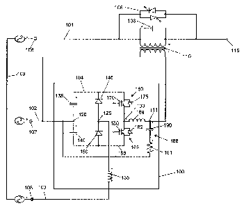
[0017] Fig. 1 is a circuit diagram illustrating one phase of a dynamic
voltage sag correction device with a series injection transformer in
accordance with
an exemplary embodiment.
[0018] Fig. 2 is a diagram illustrating a three-phase system of dynamic
voltage sag correction devices in accordance with an exemplary embodiment.
[0019] Fig. 3 is a circuit diagram illustrating a dynamic voltage sag
correction device with an input boost transformer and a series injection
transformer
in accordance with an exemplary embodiment.
[0020] Fig. 4 is a circuit diagram illustrating a dynamic voltage sag
correction device with an output boost transformer in accordance with an
exemplary
embodiment.
- 7 -
CA 02687696 2009-11-09
WO 2008/141092
PCT/US2008/063067
DETAILED DESCRIPTION
[0021] The kilovolt ampere (kVA) rating of a power electronic
switching device is a measure of the maximum capacity of the power electronic
device. In general, it is desirable to utilize the full kVA capacity of a
device to
minimize costs, optimize device performance, and optimize efficiency of the
device.
The kVA rating can be calculated for a single phase device using Equation 1
below
in which V is the maximum rms blocking voltage across the device and A is the
maximum rms current through the device. For a three-phase device, the kVA can
be calculated using Equation 2 below. It can be seen from Equations 1 and 2
that
the kVA rating and/or the kVA capability of a device is directly proportional
to the
voltage across the device. This principle can be used along with specially
configured transformers to maximize the kVA rating and/or kVA capability of
dynamic voltage sag correction devices.
Equation 1: kVA (single phase) = (V)* (A)* 1 kilo Volt
1000 Volts
Equation 2: kVA (three-phase) = (V)* (A)* 1 kilo Volt*
1000 Volts
[0022] Fig. 1 is a circuit diagram illustrating one phase of a dynamic
voltage sag correction device with a series injection transformer 110 in
accordance
with an exemplary embodiment. The dynamic voltage sag correction device
includes a regulator module 100, a static bypass switch 105, series injection
transformer 110, an output terminal 115, and a three-phase input. The three-
phase
input, which can be provided by a utility company, a generator, etc., can be
received at an input terminal 106, an input terminal 107, and an input
terminal 108.
The three-phase input also includes a neutral line 109 such that the three-
phase
input includes four input lines. Alternatively, neutral line 109 may not be
included
and the three-phase input can include three lines. The devices described
herein
can be used to provide voltage sag correction regardless of whether a physical
neutral line is included in the input. Further, as used herein, line-to-
neutral voltage
- 8 -
CA 02687696 2009-11-09
WO 2008/141092 PCT/US2008/063067
can refer to the voltage on a single line of an input regardless of whether
the input
includes a physical neutral line. An AC bus line 101 is connected to input
terminal
106 to receive a first operating signal of the three-phase input, an AC bus
line 102
is connected to input terminal 107 to receive a second operating signal of the
three-
phase input, and an AC bus line 103 is connected to input terminal 108 to
receive a
third operating signal of the three-phase input such that power can be
provided to
the system. In an exemplary embodiment, the first operating signal (along AC
bus
line 101) can have a first phase, the second operating signal (along AC bus
line
102) can have a second phase which is shifted 120 degrees from the first
phase,
the third operating signal (along AC bus line 103) can have a third phase
which is
shifted 240 degrees from the first phase.
[0023] Static bypass switch 105 can be implemented as power
transistor switching devices, a pair of thyristors connected in anti-parallel,
or any
other type of switching components known to those of skill in the art. During
normal
operation, i.e., when there is no voltage sag, static bypass switch 105 can be
closed
such that an operating signal flows directly from AC bus line 101 to output
terminal
115. When a voltage sag is detected, static bypass switch 105 can be opened by
any method known to those of skill in the art, and the operating signal from
AC bus
line 101 can be supplemented with or replaced by a correction signal which is
generated by regulator module 100 and provided through series injection
transformer 110. As such, series injection transformer 110 can be a low-duty
transformer which is bypassed and remains essentially non-energized during
normal operation. Series injection transformer 110 may only be energized
during a
sag condition. As a result, there are no continuous power losses associated
with
series injection transformer 110.
[0024] Series injection transformer 110 can include a primary winding
connected across regulator module 100 and a secondary winding connected in
series with AC bus line 101. A turns ratio of a transformer can refer to the
ratio of
turns in the primary winding to turns in the secondary winding. The turns
ratio can
be adjusted (by switching taps or switching transformers) to control a voltage
at the
- 9 -
CA 02687696 2009-11-09
WO 2008/141092 PCT/US2008/063067
secondary winding. In an exemplary embodiment, series injection transformer
110
can be used to step down (or reduce) the correction signal such that a load
connected at output terminal 115 is provided with the proper voltage during a
voltage sag. For example, series injection transformer 110 can be a step-down
transformer capable of reducing a voltage of 208 V produced by regulator
module
100 into a voltage of 120 V or less for use by the load.
[0025] Regulator module 100 is used to generate and provide the
correction signal to series injection transformer 110. In an exemplary
embodiment,
regulator module 100 can include a half-bridge inverter. Regulator module 100
is
connected to the three-phase input through a line-to-line connection with AC
bus
line 102 and AC bus line 103. Using a direct line-to-line connection without a
step-
down transformer (or as opposed to a line-to-neutral connection) results in an
increased input voltage to regulator module 100. For example, the three-phase
input may be a 120 V input used to provide a 120 V operating signal to the
load
connected at output 115. With a line-to-neutral connection (or a transformer
which
steps the voltage down to line-to-neutral), regulator module 100 is only
provided
with an input voltage of 120 V. With the line-to-line connection illustrated
in Fig. 1,
regulator module 100 is provided with an input voltage of (120 V)* (V3) = 208
V. As
such, regulator module 100 can be rated for at least 208 V, and the kVA of the
dynamic voltage sag correction device is increased.
[0026] Regulator module 100 includes a storage node 120, a rectifying
node 125, and an inverting node 130. Storage node 120 receives an input from
AC
bus line 102, and is a connecting point between a first storage unit 135 and a
second storage unit 140 which is in series with first storage unit 135. In an
exemplary embodiment, first storage unit 135 and second storage unit 140 can
be
any type of capacitor(s) known to those of skill in the art. First storage
unit 135 and
second storage unit 140 can accumulate and store energy in the form of
electrical
charges during normal operation of the system. These stored charges can be
released during a voltage sag to supplement or replace a voltage provided to
output
terminal 115 through AC bus line 101. In an alternative embodiment, first
storage
- 10 -
CA 02687696 2009-11-09
WO 2008/141092
PCT/US2008/063067
unit 135 and/or second storage unit 140 can be any other type of energy
storage
device known to those of skill in the art.
[0027] Rectifying node 125 receives an input from AC bus line 103,
and is a connecting point between a first rectifying device 145 and a second
rectifying device 150 which is in series with first rectifying device 145.
First
rectifying device 145 and second rectifying device 150, which form a
rectifying
bridge, conduct current in the same direction (i.e., first rectifying device
145
conducts current in a direction away from rectifying node 125 and second
rectifying
device 150 conducts current in a direction toward rectifying node 125). As
such,
first rectifying device 145 can be used to charge first storage unit 135 and
second
rectifying device 150 can be used to charge second storage unit 140 as known
to
those skilled in the art. As a result, regulator module 100 can be used to
provide a
correction signal which is approximately double the received input voltage
such that
voltage sags down to 50% of nominal voltage can be fully corrected. A charging
inductor 155 can be used to limit current surges into the rectifier bridge and
protect
the circuit elements upon a sudden increase in line-to-line voltage. The
sudden
increase in line-to-line voltage may occur at startup and/or when a voltage
sag
condition ends. In one embodiment, a soft charging circuit as known to those
skilled in the art can be used during startup to prevent undesirable current
surges.
In an exemplary embodiment, first rectifying device 145 and/or second
rectifying
device 150 can be semiconductor diodes. Alternatively, the rectifying devices
can
be any other devices capable of rectifying the AC line-to-line input signals
from AC
bus line 102 and AC bus line 103.
[0028] Inverting node 130 is in electrical communication with series
injection transformer 110, and is a connecting point between a first inverter
switching device 160 and a second inverter switching device 165 which is in
series
with first inverter switching device 160. First switching device 160 includes
a first
transistor 170 and a first diode 175 connected in anti-parallel with first
transistor
170. Second switching device 165 includes a second transistor 180 and a second
diode 182 connected in anti-parallel with second transistor 180. In an
exemplary
- 11 -
CA 02687696 2009-11-09
WO 2008/141092 PCT/US2008/063067
embodiment, first transistor 170 and/or second transistor 180 can be insulated
gate
bipolar transistors (IGBTs). Alternatively, any other type(s) of transistors
can be
used. During a voltage sag, a device controller can be used to control first
inverter
switching device 160 and second inverter switching device 165 such that an
adequate correction signal is generated from the charges stored in first
storage unit
135 and second storage unit 140. In an alternative embodiment, first inverter
switching device 160 and/or second inverter switching device 165 can be
implemented using any other components and/or by any other method known to
those of skill in the art.
[0029] First storage unit 135 and second storage unit 140, first
rectifying device 145 and second rectifying device 150, and first inverter
switching
device 160 and second inverter switching device 165 are connected in parallel
through a first bus line 184 and a second bus line 186. A low pass filter 188
is
connected at inverting node 130 between first inverter switching device 160
and
second inverter switching device 165. Low pass filter 188 includes a filter
inductor
189, a filter capacitor 190, and a filter resistor 191. In an exemplary
embodiment,
low pass filter 188 can be used to filter high frequency switching components
from
the AC correction signal which is provided by regulator module 100 to series
injection transformer 110. As such, series injection transformer 110 is in
electrical
communication with the inverter switching devices through low pass filter 188.
As
used herein, electrical communication can refer to any direct or indirect
electrical
connection.
[0030] In an exemplary embodiment, the dynamic voltage sag
correction device can also include the device controller (not shown). The
device
controller can be implemented as one or more programmable integrated circuits,
discreet analog circuit components, discreet digital circuit components, or
any
combination thereof. The device controller can be used to control charging of
the
storage units, detect a voltage sag, and control opening and closing of static
bypass
switch 105. The device controller can also be used to control the inverter
switching
devices to generate an appropriate correction signal to supplement or replace
the
- 12 -
CA 02687696 2015-02-19
input operating signal such that a load at output terminal 115 can continue
receiving
adequate power without interruption. The correction signal generated by the
inverter
switching devices can have a voltage which, after being stepped down by series
injection transformer 110, is adequate to supplement or replace the operating
signal (if
any) provided through input bus line 101 such that the load receives
approximately the
same line-to-neutral voltage as is provided during a normal operating
condition.
[0031] As an example, during normal operation, static bypass switch 105 can
be closed such that an operating signal with a line-to-neutral voltage can be
provided
from AC bus line 101 directly to a load connected to output terminal 115. At
any time
during normal operation, first storage unit 135 and second storage unit 140
can be
fully charged through AC bus line 102 and AC bus line 103. The device
controller can
continually monitor the operating signal for a voltage sag. The operating
signal can be
monitored at input terminal 106, at output terminal 115, at any location along
AC bus
line 101, and/or at any other location. In one embodiment, the device
controller can
identify a voltage sag when the operating signal is less than a predetermined
percentage of the normal operating signal value. For example, a voltage sag
may be
identified when the operating signal at output terminal 115 drops below 90% of
the
normal operating signal value. Alternatively, the predetermined percentage can
be any
other value. The device controller can detect the voltage sag using one or
more
comparators, logic gates, analog devices, or any other method(s) known to
those of
skill in the art.
[0032] When a voltage sag is detected, the device controller can use
additional
logic to determine the value of a correction signal such that a combination of
the
operating signal provided through AC bus line 101 and the correction signal
(after
passing through series injection transformer 110) results in a signal which is
equal to
or close to the normal operating signal value. The device controller can
13
CA 02687696 2009-11-09
WO 2008/141092 PCT/US2008/063067
control first inverter switching device 160 and second inverter switching
device 165
such that an adequate AC correction signal is generated by alternating
discharges
from first storage unit 135 and second storage unit 140. In an exemplary
embodiment, first storage unit 135 and second storage unit 140 can also
continue
to receive charges (if available) from AC bus line 102 and AC bus line 103
during
the voltage sag. The correction signal, which can be in phase with the
operating
signal from AC bus line 101, can pass through low pass filter 188 to remove
any
high frequency switching components introduced into the correction signal by
first
inverter switching device 160 and/or second inverter switching device 165.
[0033] The correction signal can pass from low pass filter 188 to
series injection transformer 110. As illustrated in Fig. 1, a primary winding
of series
injection transformer 110 is connected across regulator module at AC bus line
102
and a regulator output 111. A secondary winding of series injection
transformer 110
is connected in series with AC bus line 101. The secondary winding is also
connected in parallel with a filter capacitor 108. Filter capacitor 108 can be
used in
combination with leakage inductance of series injection transformer 110 to
form a
second low pass filter stage which is in series with low pass filter 188. In
an
exemplary embodiment, series injection transformer 110 can step a voltage of
the
correction signal down to a voltage which is less than or equal to the line-to-
neutral
voltage used by the load connected at output terminal 115. For example, AC bus
line 101 may normally provide an operating signal of 120 V to output terminal
115.
A voltage sag can occur such that AC bus line 101 is only able to provide 80 V
to
output terminal 115. The device controller can cause the inverter switching
devices
to generate the correction signal which, after being reduced by injection
capacitor
110, is equal to approximately 40 V. Because the secondary winding of
injection
capacitor 110 is in series with AC bus line 101, the 80 V from AC bus line 101
and
the 40 V correction signal are additive, resulting in a 120 V operating signal
provided to output terminal 115.
[0034] As a result, regulator module 100 can be rated at a higher
voltage (i.e., the line-to-line voltage) than the line-to-neutral voltage of
the system,
- 14 -
CA 02687696 2015-02-19
and the kVA of the dynamic voltage sag correction device is advantageously
increased. For
example, a normal line-to-neutral voltage of AC bus line 101, AC bus line 102,
and AC bus
line 103 can be 120 V, and the line-to-line voltage across AC bus line 102 and
AC bus line
103 can be (120 V) (>/3) = 208 V. As such, first storage unit 135 and second
storage unit
140 can each be charged (to a DC voltage which is a peak voltage of the RMS
voltage of 208
V) such that an AC voltage produced by inverter module 100 is approximately
208 V. A
current value through AC bus line 101 , AC bus line 102, and AC bus line 103
can be 100 A
such that regulator module 100 can have a kVA of approximately ((208 V) * (100
A)) / 1000
= 20.8 kVA. Connecting regulator module 100 through a line-to-neutral voltage
(120 V) or
stepping the line-to-line voltage down to 120 V would result in a kVA of ((120
V) (100 A)) /
1000 = 12 kVA. Thus, using the line-to-line voltage along with series
injection transformer
110 results in a 73.3% increase in kVA. Further, because the cost of the
dynamic voltage sag
correction device is primarily current driven, the cost of the '208 V dynamic
voltage sag
correction device with 100 A capability is only incrementally more than the
cost of the '120 V
dynamic voltage sag correction device with 100 A capability. Further yet, the
use of series
injection transformer 110 at the output of regulator module 100 allows
regulator module 100
to be used in both 120 V and 208 V (i.e., without series injection transformer
110) line-to-
neutral configurations. As a result, manufacturing costs are reduced because
less distinct
regulator modules are needed and components can be bought in greater bulk.
[0035] It is to be understood that regulator module 100 illustrated in and
described
with reference to Fig. 1 is not meant to be limiting with respect to the type,
number, and/or
arrangement of electrical components. In alternative embodiments, regulator
module 100 can
include any other number of components, any other types of components, and/or
any other
arrangement of electrical components as known to those of skill in the art. In
one
embodiment, regulator module 100 can be any of the regulator and storage
modules described
in U.S. Patent No. 6,118,676. Similarly, any of the other components
illustrated in and/or
described
CA 02687696 2015-02-19
with reference to Fig. 1 such as static bypass switch 105, device controller,
etc. can be
implemented by any other method known to those of skill in the art.
[0036] Fig. 2 is a diagram illustrating a three-phase system of dynamic
voltage sag
correction devices in accordance with an exemplary embodiment. In alternative
embodiments, the dynamic voltage sag correction devices described herein can
be used in
systems with any other number of phases. A first dynamic voltage sag
correction device
200 of the three-phase system can be used to provide a correction signal such
that a voltage
at a first output terminal 202 is maintained during a voltage sag. First
dynamic voltage sag
correction device 200 includes a first regulator module 205, a first series
injection
transformer 210, and a first static bypass switch 215. A three-phase input to
the system is
provided through an AC bus line 217, an AC bus line 219, and an AC bus line
221. First
regulator module 205 is connected to a line-to-line voltage across AC bus line
219 and AC
bus line 221. In an exemplary embodiment, first regulator module 205 can
include the
same components as regulator module 100 described with reference to Fig. 1.
Alternatively, first regulator module 205 may include any other components
which can be
used to generate a correction signal. In another exemplary embodiment, first
static bypass
switch 215, first series injection transformer 210, and first regulator module
205 can
operate the same as static bypass switch 105, series injection transformer
110, and
regulator module 100 described with reference to Fig. 1.
[0037] A second dynamic voltage sag correction device 225 of the three-
phase
system can be used to provide a correction signal such that a voltage at a
second output
terminal 227 is maintained during a voltage sag. Second dynamic voltage sag
correction
device 225 includes a second regulator module 230, a second series injection
transformer
235, and a second static bypass switch 240. Second regulator module 230 is
connected to a
line-to-line voltage across AC bus line 217 and AC bus line 221. In an
exemplary
embodiment, second regulator module 230 can include the same components as
regulator
module 100 described with reference to Fig. 1. Alternatively, second regulator
module 230
may include any other components which can be used to generate the correction
signal. In
another exemplary embodiment, second static bypass switch 240, second series
injection
transformer 235, and second regulator module 230 can operate the same as
static bypass
switch 105, series injection transformer 110, and regulator module 100
described
16
CA 02687696 2009-11-09
WO 2008/141092 PCT/US2008/063067
with reference to Fig. 1. Alternatively, second regulator module 230 may
include
any other components which can be used to generate the correction signal. In
another exemplary embodiment, second static bypass switch 240, second series
injection transformer 235, and second regulator module 230 can operate the
same
as static bypass switch 105, series injection transformer 110, and regulator
module
100 described with reference to Fig. 1.
[0038] A third dynamic voltage sag correction device 245 of the three-
phase system can be used to provide a correction signal such that a voltage at
a
third output terminal 247 is maintained during a voltage sag. Third voltage
sag
correction device 245 includes a third regulator module 250, a third series
injection
transformer 255, and a third static bypass switch 260. Third regulator module
250
is connected to a line-to-line voltage across AC bus line 217 and AC bus line
219.
In an exemplary embodiment, third regulator module 250 can include the same
components as regulator module 100 described with reference to Fig. 1.
Alternatively, third regulator module 250 may include any other components
which
can be used to generate the correction signal. In another exemplary
embodiment,
third static bypass switch 260, third series injection transformer 255, and
third
regulator module 250 can operate the same as static bypass switch 105, series
injection transformer 110, and regulator module 100 described with reference
to
Fig. 1.
[0039] The three-phase system described with reference to Fig. 2
allows the kVA to be increased in each of the three dynamic voltage sag
correction
devices. Thus, for a 120 V, 100 A line-to-neutral signal which is connected
line-to-
line as illustrated in Fig. 2, the three-phase system can have a kVA of 20.8
kVA +
20.8 kVA + 20.8 kVA = 62.4 kVA. Using a traditional line-to-neutral
configuration or
a configuration with step-down transformers at the inputs, the kVA would be 12
kVA
+ 12 kVA + 12 kVA = 36 kVA. Thus, it can be seen that the three-phase system
of
Fig. 2 provides a significant increase in kVA as compared to traditional
systems. In
an alternative embodiment, first series injection transformer 210, second
series
injection transformer 235, and third series injection transformer 255 may be
- 17 -
CA 02687696 2009-11-09
WO 2008/141092 PCT/US2008/063067
replaced by a single three-phase series injection transformer as known to
those of
skill in the art.
[0040] Fig. 3 is a circuit diagram illustrating a dynamic voltage sag
correction device 300 with an input boost transformer 305 and a series
injection
transformer 350 in accordance with an exemplary embodiment. While only a
single
phase portion is illustrated in Fig. 3, it is to be understood that dynamic
voltage sag
correction device 300 can be combined with any number of other dynamic voltage
sag correction devices for use in any multi-phase system. Alternatively,
dynamic
voltage sag correction device 300 can be incorporated into a single dynamic
voltage
sag correction device for use in a multi-phase system. For example, in a three-
phase system, the single dynamic voltage sag correction device can include
three
regulator modules and a single three-phase injection transformer.
[0041] In an exemplary embodiment, dynamic voltage sag correction
device 300 can be a single phase device for use in a three-phase system. With
the
exception of input boost transformer 305, dynamic voltage sag correction
device
300 can operate in the same manner as the dynamic voltage sag correction
device
described with reference to Fig. 1. In another exemplary embodiment, dynamic
voltage sag correction device 300 can be used to ensure that a load connected
to
an output terminal 310 is provided with an adequate operating voltage in the
event
of a voltage sag along an AC input bus 315.
[0042] Input boost transformer 305 can be used to boost a line-to-line
voltage input to a regulator module 320 of dynamic voltage sag correction
device
300. The line-to-line voltage input is obtained from the voltage across an AC
input
bus 325 and an AC input bus 330. A primary winding of input boost transformer
305 is connected across AC input bus 325 and AC input bus 330, and a secondary
winding of input boost transformer 305 is connected across AC input bus 330
and a
rectifying node 335 of regulator module 320. As such, an output of input boost
transformer 305 goes to rectifying node 335, and a first storage capacitor 340
and a
second storage capacitor 345 are charged to a voltage which is greater than
the
- 18 -
CA 02687696 2009-11-09
WO 2008/141092 PCT/US2008/063067
line-to-line voltage across AC input bus 325 and AC input bus 330. Series
injection
transformer 350, which is in series with AC bus line 315, can be used to step
down
the voltage of a correction signal generated by regulator module 320 as
described
with reference to Figs 1 and 2. In an exemplary embodiment, a static bypass
switch
355 can be used to bypass series injection transformer 350 during normal
operation
such that series injection transformer 350 is a low-duty transformer through
which
there are no continuous power losses. During a voltage sag, static bypass
switch
355 can be opened and series injection transformer 350 can be energized.
[0043] In an exemplary embodiment, regulator module 320 can be
adapted for use in systems with a plurality of distinct input voltages. For
example, a
first input boost transformer and injection transformer combination can be
used with
regulator module 320 when used in a system with a first line-to-line voltage
input, a
second input boost transformer and injection transformer combination can be
used
with regulator module 320 when used in a system with a second line-to-line
voltage
input, and so on. In an exemplary embodiment, input boost transformer 305 can
be
a relatively small auto transformer. Alternatively, input boost transformer
305 can
be any other type of transformer capable of boosting the voltage input to
regulator
module 320.
[0044] As an example, a line-to-neutral voltage of AC input bus 315,
AC input bus 325, and AC input bus 330 can be 120 V with a current of 100 A.
As
such, a line-to-line voltage across AC input bus 325 and AC input bus 330 is
208 V.
Input boost transformer 305 can be a 69 V auto transformer capable of stepping
the
line-to-line voltage input to regulator module 320 from 208 V up to 277 V. As
a
result, regulator module 320, which can be rated at 277 V, can be used to
provide a
correction signal in a system which has a line-to-neutral voltage of 120 V. In
a 100
A system which uses three dynamic voltage sag correction devices, the kVA is
increased 131 /0 from ((120 V)* (100 A) /1000)* 3 = 36 kVA to ((277 V)* (100
A) /
1000)* 3 = 83.1 kVA. Further, using series injection transformer 350 as
described
with reference to Figs. 1 and 2 alone or in combination with an input boost
transformer allows a single regulator module to be adapted for use in
virtually any
- 19 -
CA 02687696 2009-11-09
WO 2008/141092 PCT/US2008/063067
low voltage system. In alternative embodiments, input boost transformer 305
can
boost any line-to-line voltage by any other amount.
[0045] Fig. 4 is a circuit diagram illustrating a dynamic voltage sag
correction device 400 with an output boost transformer 405 in accordance with
an
exemplary embodiment. While only a single phase portion is illustrated in Fig.
4, it
is to be understood that dynamic voltage sag correction device 400 can be
combined with any number of other dynamic voltage sag correction devices for
use
in any multi-phase system. Alternatively, dynamic voltage sag correction
device
400 can be incorporated into a single dynamic voltage sag correction device
for use
in a multi-phase system. As an example in a three-phase system, the single
dynamic voltage sag correction device can include three regulator modules and
use
a single three-phase transformer.
[0046] Dynamic voltage sag correction device 400 includes a step-
down transformer 410, a regulator module 415, a static bypass switch 420, and
output boost transformer 405. Step-down transformer 410 can be used to reduce
a
line-to-line voltage across an AC bus line 425 and an AC bus line 430 such
that an
input voltage to regulator module 415 does not exceed a voltage rating of
regulator
module 415. As illustrated in Fig. 4, step-down transformer 410 cross couples
AC
bus line 425 and AC bus line 430 to the sag corrected line. The stepped down
input
voltage can be used to charge a first storage capacitor 435 and a second
storage
capacitor 440 of regulator module 415. During a voltage sag, static bypass
switch
420 can be opened by a device controller, and output boost transformer 405 can
be
used to step a voltage of a correction signal generated by regulator module
415 up
to a voltage which is adequate to supplement or replace a voltage of the
operating
signal (if any) which is still being provided through AC bus line 450. The
correction
signal and operating signal can be provided to a load connected to an output
terminal 445. A primary winding of output boost transformer 405 is connected
across regulator module 415, and a secondary winding of output boost
transformer
405 is connected in series with regulator module 415. In an exemplary
embodiment, output boost transformer 405 can be a relatively small auto
- 20 -
CA 02687696 2009-11-09
WO 2008/141092
PCT/US2008/063067
transformer. Alternatively, output boost transformer 405 can be any other type
of
transformer known to those of skill in the art.
[0047] As an example, regulator module 415 can be rated at 277 V. A
line-to-neutral voltage across an AC bus line 450 can be 346 V, and the line-
to-line
voltage across AC bus line 425 and AC bus line 430 can be 600 V. Step-down
transformer 410 can be used to step the 600 V line-to-line voltage down to 277
V
such that the rating of regulator module 415 is not exceeded. First storage
capacitor 435 and second storage capacitor 440 can store energy corresponding
to
the stepped down voltage such that regulator module 415 can produce a
correction
signal of approximately 277 V. During normal operation, static bypass switch
420
can be closed, and an operating signal from AC bus line 450 can be provided
directly to output terminal 445 through static bypass switch 420. Upon
detection of
a voltage sag, output boost transformer 405 can be used to increase the 277 V
provided by regulator module 415 to a voltage of 346 V such that the operating
signal along AC bus line 450 can be restored.
[0048] As described in the example above, use of step-down
transformer 410 and output boost transformer 405 allows a regulator module
with a
voltage rating of 277 V to provide a 346 V correction signal to supplement
and/or
replace the line-to-neutral voltage along AC bus line 350. Thus, in addition
to the
ability to be adapted for use in virtually any low voltage system as described
with
reference to Figs. 1-3, the '277 V' regulator module can also be adapted for
use in
high voltage systems. This further reduces manufacturing costs because a
single
regulator module can be adapted for use with in systems with a wide array of
input
voltages. In alternative embodiments, the regulator module adapted for use in
a
plurality of systems may not be rated at 277 V, but can have any other voltage
rating as known to those of skill in the art.
[0049] In an alternative embodiment, the dynamic voltage sag
correction device illustrated with reference to Fig. 4 can be adapted to
provide sag
correction in systems which operate at other voltages. As an example,
regulator
- 21 -
CA 02687696 2009-11-09
WO 2008/141092 PCT/US2008/063067
module 415 can have a voltage rating of 277 V and the line-to-neutral voltage
across AC bus line 450 can be 240 V. As such, the line-to-line voltage across
AC
bus line 425 and AC bus line 430 can be 415 V. Step-down transformer 410 can
be
used to step the 415 V line-to-line voltage down to the regulator module
voltage
rating of 277 V such that the full kVA rating of regulator module 415 is
utilized.
Instead of auto boost transformer 415, an auto buck transformer can be used to
buck the voltage at the output of regulator module 415 from 277 V down to
approximately 240 V such that the operating signal on AC bus line 450 can be
adequately corrected. The auto buck transformer can be connected at the output
as known to those skilled in the art. In an alternative embodiment, step-down
transformer 410 and the auto buck transformer can be configured for providing
voltage sag correction for different operating signal values and/or for
regulator
modules with different kVA ratings.
[0050] The foregoing description of exemplary embodiments has been
presented for purposes of illustration and of description. It is not intended
to be
exhaustive or limiting with respect to the precise form disclosed, and
modifications
and variations are possible in light of the above teachings or may be acquired
from
practice of the disclosed embodiments. It is intended that the scope of the
invention
be defined by the claims appended hereto and their equivalents.
- 22 -