Note : Les descriptions sont présentées dans la langue officielle dans laquelle elles ont été soumises.
CA 02692152 2009-12-21
WO 2009/006469 PCT/US2008/068901
TRANSMITTER SYSTEM, METHOD OF INDUCING A TRANSIENT
ELECTROMAGNETIC FIELD IN AN EARTH FORMATION, METHOD OF
OBTAINING A TRANSIENT ELECTROMAGNETIC RESPONSE SIGNAL, AND
METHOD OF PRODUCING A HYDROCARBON FLUID
FIELD OF THE INVENTION
The present invention relates to a transmitter system and a method for
inducing a
transient electromagnetic field in an earth formation.
In another aspect, the invention relates to a method of obtaining a transient
electromagnetic response signal from an earth formation.
In still another aspect, the invention relates to a method of producing a
mineral
hydrocarbon fluid from an earth formation.
BACKGROUND OF THE INVENTION
US Patent 7,053,622 discloses equipment and a method for mapping the geology
in
an underground formation, including a transmitter circuit with a current
source for
generating an electric current and a transmitter coil; a switch for connecting
the current
source to the transmitter coil during operation so that an electric current is
generated in it,
with the current building up a magnetic field in the formation, and for
cutting off this
current again so that the built-up magnetic field in the formation decays.
The current that needs to be cut-off can be high, for example 50 A or 70 A. US
Pat.
`622 proposes to use a metal-oxide-semiconductor field effect transistor
(MOSFET), or an
insulated gate bipolar transistor (IGBT), but recognizes a problem that none
of the
available switches satisfies all desired requirements, including sufficiently
high break-
down voltage, capability of switching sufficiently high currents, and having
sufficiently
low leakage current. Hence a choice has to be made regarding the balance of
properties of
the switch.
It is an object to provide a transmitter system and a method for inducing a
transient
electromagnetic field in an earth formation that does not need to be
constrained to the
choice as described, or is at least constrained to a lesser extent.
SUMMARY OF THE INVENTION
In one aspect, the invention provides a transmitter system for inducing a
transient
electromagnetic field in an earth formation, comprising: an inductive element
to generate
an electromagnetic field in response to a flow of electric current through the
inductive
1
CA 02692152 2009-12-21
WO 2009/006469 PCT/US2008/068901
element; and switching means arranged to interrupt the flow of electric
current through the
inductive element, which switching means comprises a primary switch and an
auxiliary
switch arranged in series connection with each other.
In another aspect, the invention provides a method of inducing a transient
electromagnetic field in an earth formation, comprising the steps of:
providing, in a vicinity
of the earth formation, inductive element to generate an electromagnetic
field; allowing an
electric current to flow from a power supply through a primary switch, an
auxiliary switch,
and the inductive element; and terminating the electric current from flowing
through the
inductive element by opening the primary switch and opening the auxiliary
switch.
In still another aspect, the invention provides a method of obtaining a
transient
electromagnetic response signal from an earth formation, comprising the steps
of: bringing
a receiver antenna in the earth formation; bringing, in the earth formation, a
transmitter
antenna comprising an inductive element to generate an electromagnetic field;
allowing an
electric current to flow from a power supply through a primary switch, an
auxiliary switch,
and the inductive element; terminating the electric current from flowing
through the
inductive element by opening the primary switch and opening the auxiliary
switch; and
receiving a transient response signal following the terminating of the
electric current,
employing the receiver antenna.
In yet another aspect, the invention provides a method of producing a mineral
hydrocarbon fluid from an earth formation, the method comprising steps of:
drilling a well
bore in the earth formation; providing, in the well bore, an inductive element
to generate an
electromagnetic field; allowing an electric current to flow from a power
supply through a
primary switch, an auxiliary switch, and the inductive element; terminating
the electric
current from flowing through the inductive element by opening the primary
switch and
opening the auxiliary switch; receiving a transient response signal following
the
terminating of the electric current; further processing the transient response
signal to locate
the mineral hydrocarbon fluid in the earth formation; continuing drilling the
well bore to
the hydrocarbon fluid; and producing the hydrocarbon fluid.
A geosteering cue may be derived from the further processing, whereby the
continued drilling may be responsive to the geosteering cue.
BRIEF DESCRIPTION OF THE DRAWINGS
The present invention is described in more detail below by way of examples and
with reference to the attached drawing figures, wherein:
2
CA 02692152 2009-12-21
WO 2009/006469 PCT/US2008/068901
FIG. 1A schematically shows a coil connected to a power supply and a snubber
circuit;
FIG. 1B schematically shows an electrical equivalent circuit corresponding to
FIG.
1A;
Fig. 2 shows a graph of calculated voltage Vc(t) across the coil in FIG. 1A as
a
function of time t following switching;
FIG. 3 schematically shows the coil system of FIG. 1A provided with a
switching
means comprising a primary switch and an auxiliary switch;
FIG. 4 schematically shows an embodiment of the switching means employed in
FIG. 3;
FIG. 5 schematically shows another embodiment of the coil system of FIG. 1A
provided with a switching means comprising a primary switch and an auxiliary
switch;
FIG. 6 schematically shows an embodiment employing an opto-coupler;
FIG. 7 schematically shows a drilling system;
Fig. 8 schematically shows a segmented transmitter system connected to a power
supply;
FIG. 9 schematically shows a view of helically wound groups of coil windings;
FIG. 10 schematically shows a model of a transmitter system comprising 5
groups
of coil windings;
FIG. 11 schematically shows a transmitter system representative of a class of
other
embodiments;
FIG. 12 schematically shows a transmitter system representative of another
class of
other embodiments;
FIG. 13 schematically shows a transmitter system representative of still
another
class of other embodiments; and
FIG. 14 shows an alternative snubber circuit employing a Zener diode.
DETAILED DESCRIPTION OF THE INVENTION
A transmitter system is disclosed, for inducing a transient electromagnetic
field in
an earth formation. Such a transmitter may be incorporated and/or used in a
tool and/or
method for transient electromagnetic (EM) logging, which provides information
on
electromagnetic properties of a formation around the tool at various distances
from the
tool. In this transient EM method, a transmitter antenna is energized which
energizing is
3
CA 02692152 2009-12-21
WO 2009/006469 PCT/US2008/068901
generally terminated after which a temporal change of signal (e.g. voltage)
induced in a
receiver antenna is monitored over time.
The transmitter and receiver antennae may typically be provided in the form of
coils as described in, for instance, US patent application publications
2005/0092487,
2005/0093546, and 2005/078481, and in US Patent 5,955,884, each incorporated
herein by
reference. On the transmitter end, such a coil represents an inductive element
and thus it
forms an inductive load.
It is now proposed to interrupt the flow of electric current through an
inductive
element using switching means that comprise a primary switch and an auxiliary
switch
arranged in series connection with each other, and delay circuitry to impose a
time delay
between switching of the auxiliary switch relative to switching of the primary
switch.
Provision of a primary and an auxiliary switch provides more versatility in
designing the switching means to fulfill desired requirements. It allows for
combining
favorable properties of the primary switch with other favorable properties of
the auxiliary
switch. The favorable properties of the auxiliary switch may be complementary
to those of
the primary switch, for instance to compensate for a less favorable property
of the primary
switch, which allows an ability of disregarding that property when selecting
the type of
primary switch to employ.
As an example, this concept may be applied in the following situation. When
the
flow of current through such an induction coil is rapidly turned off or
terminated, a voltage
spike is built across the coil due to back-electromagnetic force (back-EMF or
counter-
EMF) effects. This voltage spike may exceed maximum tolerances of one or more
of the
components in the tool. In such a case, the switching means may comprise a
primary
switch with a high break-down voltage, optionally combined with an ability to
cut-off a
high current. Any adverse property of such a primary switch, such as possibly
a high
leakage current or tailing current, may be compensated by selecting the
auxiliary switch to
provide that function.
Delay circuitry may be provided to impose a time delay between switching of
the
auxiliary switch relative to switching of the primary switch. Opening the
auxiliary switch
after opening the main switch, helps to ensure that the auxiliary switch is
not exposed to
any adverse back-EMF voltage. Since the primary switch may have already dealt
with the
voltage spike and/or the cutting off of a high current, the auxiliary switch
does not have to
possess such capabilities.
4
CA 02692152 2009-12-21
WO 2009/006469 PCT/US2008/068901
The primary switch may, as a result, be selected due to its favorable
breakdown
properties (e.g. high breakdown voltage) without also considering all the
other relevant
properties such as low leakage current, because the auxiliary switch may be
selected on the
basis of other properties such as a low leakage current. If such other
property will be
contributed to the switching means by the auxiliary switch, the primary switch
does not
have to have a favorable leakage current.
Stated more generally, if at least two specified electrical characteristics
are of
interest, the switching means could be favorable in respect of both these
characteristics
whereby one of the electrical characteristics of the switching means is
attributable to a
corresponding electrical characteristic of the primary switch and the other
one is
attributable to a corresponding characteristic in the auxiliary switch.
In logging while drilling (LWD) applications, it is advantageous to detect the
presence of a formation anomaly ahead of a drill bit or around a bottom hole
assembly.
U.S. patent application published under number 2006/0038571 describes methods
for localizing an electromagnetic anomaly in a subterranean earth formation,
employing
transient electromagnetic methods. These methods particularly enable finding
direction and
distance from a transient electromagnetic measurement tool to a resistive or
conductive
anomaly in a formation surrounding a borehole in drilling applications.
In these methods, typically a tool, comprising a transmitter coil and a
receiver coil,
is lowered into a borehole in the earth formation. The transmitter coil
produces a magnetic
dipole field in the formation. Due to, for instance geometric properties of
the transmitter
system, in practice the dipole field will be an approximate dipole field. A
transient
response signal, comprising an induced voltage in the receiver coil, is
measured after
rapidly turning off the current that is passed through the transmitter
antenna. The sudden
drop is understood to generate decaying eddy currents in the formation, which
in turn
induce the transient response signal at the receiver antenna.
The referenced US patent application shows that relevant conductivity
information
of the earth formation is embodied in the response signals over the entire
time span of the
decay, starting already during the first microseconds after the sudden drop in
the current
and continuing up to perhaps even seconds.
The coils may be wound coaxially around a longitudinal axis of a down-hole
tool,
or they may be provided in another way. Examples include winding at an angle
relative to
the longitudinal axis of the down-hole tool, or winding according to a so-
called saddle coil
5
CA 02692152 2009-12-21
WO 2009/006469 PCT/US2008/068901
configuration whereby the windings of the coil do not fully encircle the
longitudinal axis of
the down-hole tool. Energizing of the transmitter antenna may be accomplished
by
applying a current through a transmitter coil. The current applied at a
transmitter antenna is
generally terminated to terminate the energizing.
Figs. 1A and 1B schematically show a transmitter system that may be
incorporated
in a down-hole tool. Fig. 1A schematically shows a transmitter antenna in the
form of coil
4 connected to a power supply 2 via a switch 8. An optional shunt in the form
of snubber
circuit 6 is connected parallel to the coi14.
Fig. 1B shows a possible equivalent electric circuit of the comparative
example. A
physical coi14, typically not only provides an inductance L but also a non-
zero resistance R
and a distributed capacity C as shown in Fig. 1B. These properties may give
rise to a
resonance current in the coil, Ic, also indicated in Fig. 1B.
The optional snubber circuit 6 has been assumed to comprise a resistor R1 and
a
series capacitor Cl, tuned to prevent the current from oscillating as well as
to control the
current decay Ic(t) within the coi14. It could, however, include more and/or
other
components, as will be exemplified below, or the snubber circuit 6 could
consist of a
damping resistor only.
The power source 2 has been assumed to comprise of a DC voltage source 10. For
the purpose of the present specification, a DC voltage may include relatively
slowly
varying voltage waveforms compared to the desired measurement interval, or AC
waveforms with a non-zero DC offset component that is large relative to the AC
component. Slowly varying is understood to include frequencies of up to a few
Hz,
typically up to about 5 or 10 Hz, depending on the desired measurement
interval.
Preferably, the DC current is very constant and steady for at least 10 ms
prior to turn-off.
The DC voltage source 10 may be a bipolar source switched such that the
polarity
of the voltage imposed over the transmitter coil is reversed in each
subsequent energizing
cycle.
The switch 8 will be assumed to comprise of an ideal switch capable of
switching
between true zero impedance and infinite impedance states instantaneously.
When the switch has been closed (its zero impedance or zero-resistance state)
for a
sufficiently long time, a DC current I corresponding to I = V/R passes through
the coi14
causing a static magnetic field. Prior to opening switch 8, the inductor L
acts as a short due
6
CA 02692152 2009-12-21
WO 2009/006469 PCT/US2008/068901
to the DC character of the current. The voltage across the coils, Vc, is
therefore equal to the
voltage V of the source 10.
Opening switch 8, resulting in an instantaneous increase in its resistance
from
essentially zero to essentially infinite provided that the voltage across it
does not exceed a
break-down limit, would collapse the static magnetic field. Faraday's law
states that a
changing magnetic field results in an electromotive force (EMF, ~ that is
equal to the time-
derivative (d/dt) of the magnetic flux.
Since part of the flux associated with the magnetic field passes through the
coi14,
switching it off causes a back EMF. A back EMF that is too large may cause a
problem on
for instance the switch 8.
The total voltage across the coi14 is given by the sum of the back-EMF plus
R=I(t).
In an induction coil, the back-EMF may be expressed as its self-inductance L
times the
time-derivative dIc/dt of the current Ic(t). Thus, after opening the switch 8,
the EMF is
likely to become the dominant term. Since current Ic(t) is decaying, the
voltage across the
inductive load L will have a reverse polarity relative to that across the
resistor R.
As an example, Table I summarizes parameters of a transmitter coil as it might
be
employed in a down-hole transient EM tool.
Table I:
Parameter Symbol value
Coil diameter 14 cm
Number of windings N 125
Pitch of windings 2 mm
Axial length of coil f 25 cm
Self-inductance of coil L 0.95 mH
Ohmic resistance of coil R 0.46 S2
Distributed Capacitance coil C 50 pF
Snubber Resistance RI 2100 S2
Snubber Capacitance CI 1 F
Self-inductance has been derived from the dimensions using a formula in W.R.
Smythe "Static and Dynamic Electricity", third edition, Hemisphere, New York,
1989. The
ohmic resistance has been calculated assuming the coil has been formed out of
14 gauge
7
CA 02692152 2009-12-21
WO 2009/006469 PCT/US2008/068901
copper wire and assuming room temperature. The capacitance of the coil is
based on an
estimate.
The snubber resistance and capacitance have been chosen to achieve a -80 dB
attenuation of the current at 3 s after opening the switch 8.
The current Ic(t) and the voltage in the coi14 and the resulting back EMF
voltage
Vc(t) across the coil may be calculated using the equivalent electric circuit
as depicted in
Fig. 1B. The voltage across the coil, Vc(t), resulting in turning a DC current
of 6.5 A off by
a factor of -80dB in less than 3 s is shown in Fig. 2. It reveals that
switching at that rate
results in a voltage spike of about 1 kV, which is generally too much for a
typical metal-
oxide-semiconductor field-effect transistor (MOSFET), but still below break
down voltage
of some commercially available insulated gate bipolar transistors (IGBTs).
Insulated gate
bipolar transistors, known in the art as IGBT may realistically have switching
speeds of
less than 1 s, and relatively high breakdown voltage exceeding 1 W.
A switch that has a high break-down voltage allows relatively high turn-off
rates of
the current through the transmission coil, because back EMF scales with the
time
derivative of the current (dI/dt) or the self-inductance L, or both. However,
the fast, high
break-down voltage switches that are presently commercially available, e.g.
IGBTs,
typically have been found to suffer from a fairly high trailing current that
may persist
It has been found that an IGBT with a relatively fast initial turn-off time
and a high
break-down voltage, which as explained above is useful when dealing with a
relatively
high back-EMF voltage, may also suffer from a tailing current that may persist
up to
hundreds of microseconds after the initial turn-off. Such a tailing current
may be relatively
small compared to the initial current, but it may still adversely affect the
signal to noise
ratio of a transient electromagnetic logging tool since the transient response
signals from
the earth formation after a few hundred microseconds is also expected to be
very small.
The turn-off may be expedited and the signal-to-noise ratio increased by
providing,
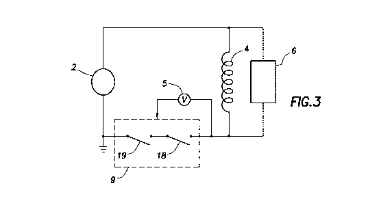
instead of a single switch 8, a switching means 9 to provide improved
switching
functionality. The switching means 9, as shown in FIG. 3, comprises a primary
switch 18
and an auxiliary switch 19 arranged in series connection with each other. The
fact that
there is a plurality of switches comprised in the switching means allows, for
instance, the
primary switch 18 to be selected on the basis of its favorable breakdown
properties (e.g.
high breakdown voltage), and the auxiliary switch 19 to be selected on the
basis of other
properties such as switching time and/or leakage current and/or tailing
current.
8
CA 02692152 2009-12-21
WO 2009/006469 PCT/US2008/068901
The example shown in Fig. 3 shows the switching means 9 in series with power
supply 2 and coi14 shunted with optional snubber 6, basically corresponding to
what was
modeled hereinabove with reference to FIGs. lAB and 2.
In order to protect the auxiliary switch from exposure to excess voltage
exceeding
its break-down voltage during turning-off, the auxiliary switch may be kept
into its low-
impedance (resistance) state for a duration of time after bringing the primary
switch 18 into
its high-impedance state before the auxiliary switch is brought into its high-
impedance
(resistance) state. In other words, a certain delay time may be applied for
switching the
auxiliary switch, which may in practice be implemented by providing delay
circuitry of
any suitable type.
There are numerous ways to implement delay circuitry, including using a
digital
signal processor (DSP) with a timer or a clock and any suitable type of
controller or micro-
controller such as a programmable interface controller (PIC).
FIG. 4 shows an embodiment of the switching means 9, wherein the primary and
auxiliary switching means are provided in the form of gate transistors. A
common gate
transistor is a field-effect transistor (FET). A gate transistor may have a
first and second
terminals connected with each other via a gated channel. These terminals may
be referred
to with various terms, of which source and drain, collector and emitter, etc.,
are examples.
The switching occurs between these terminals as a result of impedance changes
in the
gated channel, depending usually on gate potential relative to one of the
first and second
terminals (usually the drain or the emitter). A gate terminal is provided to
regulate the gate
voltage.
In FIG. 4, the primary switch 18 is provided in the form of an IGBT 27, and
auxiliary switch 19 is provided the form of a MOSFET 28. The auxiliary switch
19 may be
used to shut off the tailing current from the IGBT 27. As a result, the
residual field
generated by the coil is suppressed leading to an improved signal-to-noise
ratio.
Delay circuitry 29 is provided and arranged to delay the switching of the
auxiliary
switch 19 relative to the switching of the primary switch 18. For instance,
the primary
switch 18 may be coupled to a primary switch controller for controlling the
switching of
the primary switch, and the auxiliary switch 19 may be coupled to an auxiliary
switch
controller for controlling the switching of the auxiliary switch, wherein the
auxiliary switch
controller may be coupled to the delay circuit 29.
9
CA 02692152 2009-12-21
WO 2009/006469 PCT/US2008/068901
The delay time may be selected to be long enough for any back-EMF voltage to
fall
to a level below a predetermined value. The predetermined value may be
selected such that
there is no danger of exceeding the break-down voltage of the auxiliary
switch. In the
configuration as shown in FIGs. 3 and 4 jointly, the auxiliary switch will in
principle not
be exposed to any back EMF after the primary switch is in its high-impedance
state. In
such a case, the delay could be as close to 0 as the transition time
associated with the
primary switch switching from closed to open.
In other configurations, when at least one of the poles of the auxiliary
switch could
be exposed to the back-EMF voltage generated in the coil, e.g. as shown in
Fig. 2, the
required delay time may be found by finding the time that it takes for the
voltage to drop
below the break-down voltage of the auxiliary switch. If that is 200 V, as may
be quite
typical for a MOSFET, the delay time may for instance be chosen at 1.0 s or
longer.
More generally, if the breakdown voltage for a specific switch would be Vb, a
minimum delay time may be found in the voltage Vc(t) behavior after switching
the
primary switch to its high impedance state by finding the time tdelay after
switching of the
primary switch at which the back-EMF voltage induced in the coil across the
auxiliary
switch has decayed to below Vb.
Feedback and control means 5 may be provided, arranged to control the
switching
of the auxiliary switch in response to a signal representing actual back-EMF
voltage
generated in the inductive element as a function of time, at times after
switching of the
primary switch. For instance, a signal representing the voltage Vc(t) of FIG.
2 could be
used as the feedback signal in order to generate a trigger signal or a gate
signal that triggers
or results in the switching of the auxiliary switch.
The delay time may thus be made dependent on the decay of the back-EMF
voltage. Alternatively, the delay time may be predetermined, for instance such
as to
achieve a desired target turn-off time. When a certain attenuation of current
is desired in a
certain time, the delay time may be chosen at the desired time minus the
specified
switching time of the auxiliary switch. For example, when a -80 dB attenuation
in 3 s is
desired, the delay time may be predetermined at anywhere between 0.1 s and 3
s, or for
more typical back-EMF voltage spikes, between 1 s and 3 s.
FIG. 4 also shows optional protection shunts comprising Zener diodes 26 and
31.
Zener diode 26 directly connects the emitter of IGBT 27 to its collector and
Zener diode 31
CA 02692152 2009-12-21
WO 2009/006469 PCT/US2008/068901
connects the source to the drain of MOSFET 28. More generally, the diodes are
connected
in parallel to the primary and/or auxiliary switches and schematically
represent optional
protection circuits, which protect the switches against excess voltage
exceeding their
break-down voltage. In reality, a number of Zener diodes, or other non-linear
components,
may be used in series depending on the break-down voltage of the individual
Zener diodes.
More generally, the protection circuit shunts may comprise an active element,
for
example a diode, a varistor, a Zener diode or an avalanche diode. The
principle of
operation is that the switch is bypassed by a path which has an effective
impedance that
decreases with potential difference. Such a non-linear component ensures that
the switch is
protected against an excess voltage. A number of such active elements may be
connected
in series in order to divide the voltage drop over the number of elements.
Oscillations may
not be an issue in the switches, in which case the protection circuit may
consist of only the
active element(s). Some gated transistors have such a protection shunt built-
in, in which
case an additional protection shunt may be redundant.
Resistor 25 in FIG. 4 may be provided to keep the emitter of the IBGT close to
ground, to ensure that the gate voltage can be set relative to ground.
However, there are
other ways of referencing the gate voltage. An example will be given below
with reference
to FIG. 6.
Also shown in FIG. 4 is a potential limiting circuit 24, arranged to limit a
potential
difference between the gate terminal and the emitter terminal. In the present
case, the gate-
emitter potential determines whether the switch is open or closed. The
potential limiting
circuit 24 protects the switch against a to high potential difference, which
could burn out
the switch.
Here, the potential limiting circuit 24 is provided in the form of two Zener
diodes
arranged back-to-back such that they are blocking conduction between gate and
emitter
terminals. However the potential difference is limited to the Zener break down
voltage. For
this application, the Zener break down voltage is typically less than 20 V,
for instance
between 5 V and 15 V. We used 12 V Zener diodes as they are cheap and
effective.
However, other active components may be used, such as avalanche diodes, or
other
potential limiting circuits 24 that may be devised by a person of skill in the
art.
The primary and auxiliary switches do not have to be in direct connection with
each
other such as is the case in the embodiment of FIG. 3. For instance, as
schematically
depicted in FIG. 5, the auxiliary switch may be series connected between the
inductive
11
CA 02692152 2009-12-21
WO 2009/006469 PCT/US2008/068901
element (e.g. coi14) and one pole of the power supply 2, while the primary
switch may be
series connected to the other side of the inductive element and the other pole
of the power
supply 2. Either one of the poles of the power supply 2 may be connected to
ground.
In embodiments such as described above with reference to FIG. 5, the inductive
element has a switch on either side and can thus be cut-off entirely from
other elements or
circuitry, which may lower even further the chance of a residual magnetic
field to be
generated after turning-of However, the primary switch 18 is not commonly
grounded to
the ground to which power supply 2 is grounded. If the primary switch is based
on a gated
transistor, such as an IGBT, this may have to be taken into account when
referencing a gate
voltage.
The upper switches (upper switches are those that do not reference to the
common
ground) may have to be referenced to a separate ground from the main power
supply 2. An
example of how this may be done employing gated transistor switches 180 and
185, each
comprising a gate, an emitter and a collector, is schematically depicted in
FIG. 6.
FIG. 6 shows a group of coil windings 45, which may correspond e.g. to the
coi14
of FIG. 5, that is connected to the common ground 100 via switch 185,
hereinafter referred
to as the lower switch 185. FIG. 6 also shows the switch 180 that is connected
to the main
power supply 2. This will be referred to as the upper switch 180. For the
purpose of the
present example, upper switch 180 will be assumed to function as the primary
switch of the
switching means and lower switch 185 will be assumed to function as the
auxiliary switch.
Consistently, upper switch 180 has been depicted as an IGBT while lower switch
185 has
been depicted as a MOSFET, but the principle as will be set forth below does
not require
these specific types of switches. Moreover, the assignment of primary and
auxiliary
switching function is arbitrary chosen by way of example, and the roles may be
interchanged.
The group of coil windings 45, which will also be referred to as coil segment
45,
may constitute a full coil, or it may be one group amongst any number of
additional groups
of coil windings. In the latter case, which will be illustrated in more detail
hereinbelow
with reference to FIG. 10, additional switches may be provided between the
present coil
segment 45 and upper switch 180, as schematically indicated at 101 in FIG. 6.
The principles that will be set forth also apply for switch 180 if there would
be
another coil segment provided between switch 180 and the main power supply 2,
such as is
the case for instance with respect to switch 181 in FIG. 10 to be discussed
herein below.
12
CA 02692152 2009-12-21
WO 2009/006469 PCT/US2008/068901
An optional snubber circuit 65 is depicted connected in parallel with the coil
segment 45. Optional switch protection circuits 190 and 195 have been depicted
connecting emitter and collector of switches 180 and 185, respectively. More
details have
been provided hereinabove.
Still referring to FIG. 6, the gate voltage of the lower switch 185 is
referenced to
the potential in line 55, which is connected to the common ground 100. The
electronics
driving the gate of upper switch 180, including power supplies 112, 113 and
gate driver 90
are referenced to the potential in line 50 which is connected to the emitter
of the upper
switch 180 and acts as a "floating ground" as soon as the lower switch 185 is
open. As a
result, the gate voltage of upper switch 180 is referenced to the emitter of
upper switch
180.
The potential of the "floating ground" relative to the common ground could be
quite high, and variable, as a result of back-EMF induced by the coil
segments, when the
switches are opened. The embodiment of FIG. 6 provides an opto-coupler 114, to
electrically isolate other controller electronics (including, e.g.,
microcontroller 11 of FIG.
10) from the floating ground. Such an opto-coupler is also shown at 119 for
the lower
switch, as an option.
An opto-controller essentially comprises a controllable light source, here
shown in
the form of a light emitting diode (LED) 124, 129, in optical communication
with a light
detector, where shown in the form of a photo-diode 125, 130. The LED and photo
diode
may be in each other's near vicinity, such as integrated on the same circuit
board or micro-
electronic chip, or at remote distances with a light-conducting medium between
them such
as an optical fiber, or in any other configuration. A suitable integrated opto-
coupler is
available as part number PS8601.
If the microcontroller 11 cannot source enough current to drive the opto-
controllers,
an intermediate switch 121, 126 may be provided in between. Such intermediate
switch
may be provided in the form of a relay, an amplifier, a switching transistor
or other suitable
arrangement. Here, as an example, the intermediate switch is provided in the
form of a
switching transistor 122, 127, the base thereof being connected to the
microcontroller 11
output, via for instance a resistor, and an amplifier power supply 123, 128.
The amplifier
power supplies may be provided in the form of one power supply supplying the
power for
all or a plurality of the amplifiers 121, 126. This way, light generation in
the LEDs 124,
129 may be activated using the microcontroller 11.
13
CA 02692152 2009-12-21
WO 2009/006469 PCT/US2008/068901
The photo diodes 125, 130 are arranged to activate another intermediate
switch,
here provided in the form of a second switching transistor 131, 136 arranged
to be biased
by the photo diode 125, 130 in combination with a power supply 113, 118. Lines
135 and
139 connect the second switching transistor 131, 136 to their respective gate
driver 90 and
95, which are powered by power supplies 112 and 117, respectively. The gate
drivers 90,
95 put the gates of switches 180 and 185 on a controlled voltage referenced to
lines 50, 55.
A resistor R4 may be provided between each of lines 135 and 139 and their
respective
power supply 113 and 118.
An optional voltage divider, e.g. consisting of two resistors R2 and R3, may
also be
provided between the gate driver 90, 95 the switches 180, 185 and the floating
grounds 50,
55 if needed, e.g. to enhance stabilization. Typically, one might choose R3 >>
R2, e.g. R3
is a few kS2 and R2 a few S2.
Also, a potential limiting circuit 134 may be provided to ensure that the
potential
difference between the gate terminal 137 and the emitter terminal of the IGBT
180 stays
within a window set by the circuit.
In operation, a low pulse from the microcontroller causes the transistor 122,
127 to
switch on and activate light generation in the LED 124, 129. The collector of
the second
switching transistor 131, 136 thus goes high for the duration of the initial
low pulse from
the microcontroller 11, turning the respective gate 137, 141 of the IGBT 180,
185 on for
the duration of the in initial low pulse. This brings the switches into their
low-impedance
condition and the coil segment 45 is energized at a level determined by the
current
delivered by the main power supply 2.
The outputs of the microcontroller 11 are then brought to high, turning the
IGBTs
off and thereby creating the transient electromagnetic field. A transient
response signal
may be recorded at this time. The microcontroller 11 could be programmed such
as to
bring the high output on the line leading to the switch that functions as the
auxiliary switch
(here: switch 185) at a later time than when the high output was brought on
the line leading
to the switch that functions as primary switch (here: switch 180).
The operation may be repeated over and over again for as long as desired.
Optional capacitors 142 may be provided through-out, to bleed off any AC
components from the circuitry to the floating ground. Their capacitance values
would be
easy to determine based on the specific characteristics of an embodiment.
14
CA 02692152 2009-12-21
WO 2009/006469 PCT/US2008/068901
A transmitter system in accordance with the principles set forth above, may be
employed to obtain a transient electromagnetic response signal from an earth
formation.
Such a response signal may be sensed after terminating the current, by a
receiver antenna
that is brought into the earth formation, for instance via a bore hole or a
well bore. The use
of the delayed auxiliary switch as set forth above is applicable to switching
of induction
elements including coils.
Fig. 7 shows a down-hole too130 for such transient electromagnetic induction
measurements of an earth formation 32. The down-hole tool is adapted to fit
inside a
typical bore-hole in an earth formation. In the embodiment as shown, the down-
hole tool
30 is incorporated in a drill string 33 supporting a drill bit 38 in a bore-
hole 39. A reservoir
containing a mineral hydrocarbon fluid 34 is also present.
The down-hole too130 may typically be included in a bottom hole assembly (BHA)
as part of a logging while drilling (LWD) tool and/or of a measurement while
drilling
(MWD) tool. The tool may be used in logging and/or measurement while drilling
applications, including geo-steering, reservoir delineation and geo-pressure
detection.
In other embodiments, the down-hole tool may be suspended in the bore-hole 39
on
a wire line. Wire line tools as such are known: one is shown and described in
US Pat.
6,952,101, of which the contents are herein incorporated by reference.
The down-hole too130 as depicted in present Fig. 7 comprises a transmitter
system
comprising transmitter antenna 35 and a sensor in the form of a receiver
antenna 36
displaced from the transmitter antenna 35 at a predetermined offset. A
predetermined
offset, however, is not a requirement of the invention. The transmitter
antenna may
comprise a coil with a number of windings to generate essentially a magnetic
dipole field.
The number of number of windings is optionally divided into two or more groups
of
windings 35, 35', arranged to cooperatively generate the essentially magnetic
dipole field
when energized. Further details on dividing the windings into groups of
windings will now
be provided, with reference to FIGs. 8 to 13. The coils may be solenoid coils
and, likewise,
the groups of windings may also be solenoidal of nature.
It has been estimated that, detecting a resistivity anomaly up to 50 to 100 m
away
from the tool out in the formation using a transmitter coil and a receiver
coil as the
antennae, a magnetic moment of 50 A=m2 in the transmitter coil and an
effective area of
100 m2 in the receiver coil would be sufficient. For the purpose of down-hole
CA 02692152 2009-12-21
WO 2009/006469 PCT/US2008/068901
investigations, a magnetic moment of between 1 A=m2 and 1000 A=m2 has found to
be
generally practicable.
Moreover, for detecting the anomaly close by the tool, a turn-off time of 3 s
may
be desired to be able to measure its electromagnetic properties without
contribution from
the transmitter coil still generating a field.
The magnetic moment, m, of a coil is given by:
m=N=s=I (1)
wherein N is the number of windings in the coil, s is the cross-sectional area
of the air-core
defined by the windings, and Ithe current passed though the coil.
To generate a magnetic moment of 50 A=m2 using the coil as summarized in Table
I above, a DC current of 26 A must be passed through it.
As stated before, back-EMF scales with the time derivative of the current
(dI/dt) or
the self-inductance L, or both. Thus, switching 26 A instead of the 6.5 A in
the same time
as was used for calculating FIG. 2, the back-EMF would exceed the
approximately 1kV of
FIG. 2, which could pose a problem for the switching means used. At first
glance, instead
of increasing the current one could consider increasing N or s. However, that
would not
solve the issue because the self-inductance of an air-core coil, which may be
approximated
by:
L ,z~ ,uoN2s l f (2)
wherein ,up is the free-space magnetic permeability and t is the length of the
coil, would
increase leading to increased back EMF as well. At first glance, it appears
that L can be
reduced by simply decreasing N or s.
A solution to this problem of inducing a transient electromagnetic field in an
object,
is provided by dividing the number of windings of the transmitter coil into
two or more
groups of windings arranged to cooperatively generate the essentially magnetic
dipole field
when energized, and to provide switching means arranged to essentially
simultaneously
terminate the energizing of at least two of the groups of windings. The entire
arrangement
is such that, at least when the energizing is terminated, the groups of
windings are
electrically isolated from each other or connected in parallel with each
other.
Herewith it is avoided that groups of windings are connected in series with
one or
more other groups of windings after terminating the energizing. By avoiding
that groups of
16
CA 02692152 2009-12-21
WO 2009/006469 PCT/US2008/068901
windings are connected in series with one or more other groups of windings
after
terminating the energizing, the back-EMF voltage is lowered.
This lowers the back-EMF voltage because the total voltage is divided over the
groups of coils. Moreover, dividing the coil into groups of windings allows
optimization of
the geometry such that the mutual induction between the groups is lowered,
resulting in an
even lower back-EMF voltage altogether.
Fig. 8 schematically shows a transmitter system, wherein the inductive load 4
is
provided in the form of two or more energizable inductive segments. In the
embodiment of
Fig. 8, the inductive load is provided in the form of coi14 (similar to coi14
of Fig. 1A), the
windings of which have been divided into three groups of windings (unlike the
coi14 of
Fig. 1A) to form inductive segments 41, 42, and 43. The groups of windings in
the
embodiment of Fig. 8 each are connected to a shunt circuit in the form of an
optional
snubber circuit 61, 62, 63, arranged in parallel connection to the respective
groups of
windings. The snubber circuit may damp an internal resonance of the group of
windings.
In the present example, the windings of the coi14 have been divided into three
equal groups, but this is not a requirement of the invention. The division
into groups may
be into a different number of groups and/or the groups having mutually
different numbers
of groups of windings. For instance, in a co-axial arrangement of the groups
of windings, a
group that is centrally located relative to the other groups may need fewer
windings in
order to possess the same induction as the other groups.
The segments (groups of windings) 41 to 43 are connected in series with each
other. Each segment also comprises a switch 81, 82, 83, in series with the
segments.
The groups of windings 41, 42, 43, together with the switches, are series
connectable with the power source 2 to energize them. An optional additional
switch 81' is
provided as well, in order to enable full isolation of each of the groups of
windings from
the power supply when energizing is terminated. If such an optional additional
switch is
provided, one of the switches may function as a primary switch and one as an
auxiliary
switch as has been detailed hereinabove. Alternatively, any one of switches
81, 82, 83 may
be embodied as or replaced by a switching means 9 as shown in FIG. 3 and/or
FIG. 4.
The switches 81, 82, 83, and in this embodiment also switch 81', are
controlled by
a common controller 11. The common controller 11 may be used to concertedly
trigger
switching of the switches 81, 82, and 83 into switching into their high-
impedance state
essentially simultaneously. Optional switch 81' may also be switched
essentially
17
CA 02692152 2009-12-21
WO 2009/006469 PCT/US2008/068901
simultaneously but that is not necessary. It may even be desired to purposely
delay the
switching of one of the switches into its high-impedance state for a certain
period of time
after switching the other switches.
When the switches are all in their conducting state, more generally stated
their low-
impedance state, the coil segments are energized by the power supply 2. The
coil segments
41, 42, and 43 are arranged to cooperatively generate the essentially magnetic
dipole field
when energized. In the example, the coil segments are wound coaxially around a
common
axis A, and the current is directed in the same way such that the magnetic
moments add up.
When all switches are open (non- or low conducting state), the groups of
windings
are electrically isolated from each other and from the power supply 2. The
back-EMF
voltage spike is thus divided over the coils/switches.
The coil segments 41, 42, 43 need only be electronically separated from each
other,
not physically. The coil segments 41, 42, 43 may also be wound concentrically
one on
another, or as multiple helixes interlaced with each other, such as shown in
FIG. 9.
However, physical separation may be beneficial in that it reduces mutual
inductance
between the group of windings of the coil.
Generally, when a coil is divided into S segments, such as by dividing the
number
of windings into S groups of windings, the self-inductance of the total coil
is the sum of the
self-inductances of each segment and all the mutual cross inductances between
the
segments.
For instance, the 125-winding coil (corresponding to Table I) may be divided
into
equal segments 41,42,43. The total coil length remains the same, because the
coil segments
are abutting to each other. The self-inductance of each segment is
approximately one fourth
of the value of that of the total coil. The remaining one fourth arises from
the mutual cross
inductances between the segments. These follow from formulas known to the
person of
ordinary skill in the art. The ohmic resistance R of each coil segment is
simply one third of
that of the full 125 winding coil. The distributed capacitance C of each coil
segment is
more difficult to estimate. It will be assumed to be one third of the full
value of Table I.
This is not a crucial point, because the segment capacitance may be adjusted
by adding a
shunt in parallel.
Each segment may further comprise a snubber circuit 61, 62, 63 consisting of a
resistor and a capacitor. An overview of the dimensions and parameters are
given in Table
II in respect of the segments.
18
CA 02692152 2009-12-21
WO 2009/006469 PCT/US2008/068901
Table 11:
Parameter value
segment diameter 14 cm
Number of coil segments 3
Number of windings per segment 42
Pitch of windings 2 mm
Axial length of each segment 8.4 cm
Self-inductance in segment 0.23 mH
Ohmic resistance of segment 0.15 S2
Distributed Capacitance segment 17 pF
Snubber 61 Resistance 900 S2
Snubber 62 Resistance 1000 S2
Snubber 63 Resistance 900 S2
Snubber 61 Capacitance 2 F
Snubber 62 Capacitance 2 F
Snubber 63 Capacitance 2 F
Cross inductance segments 41-42 0.060 mH
Cross inductance segments 42-43 0.060 mH
Cross inductance segments 41-43 0.012 mH
Effective inductance segment 41 0.30 mH
Effective inductance segment 42 0.35 mH
Effective inductance segment 43 0.30 mH
The effective inductances of each segment, being the self-inductance of the
segment plus the mutual cross inductances arising from the other segments,
have been
calculated assuming that the currents in the segments are equal to each other.
Thus, the
voltage across each segment is the sum of the EMF plus R=Ic(t), whereby the
EMF may be
expressed as the effective self-inductance times the time derivative dIc/dt of
the current
Ic(t) in the coil segment.
Since the total coil is essentially equal to the one of Table I, the same
current
passing through it energizes the magnet to the same magnetic moment as the
undivided
coil. By dividing the large coil into even more and smaller segments, the
voltage across
19
CA 02692152 2009-12-21
WO 2009/006469 PCT/US2008/068901
each segment, and therefore each switch, will be reduced. An example employing
gated
transistor switches for controlling a coil divided into five segments will now
be discussed.
Fig. 10 shows a schematic model of a transmitter system comprising a power
supply 2 and 5 inductive segments (41 to 45), switches (181 to 185) in the
form of IGBTs
associated with each of the inductive segments and functioning as primary
switches, and an
additional auxiliary switch 180 to enable full isolation of all the inductive
segments from
the power supply 2 including segment 41. Here, the auxiliary switch has been
depicted as
an IGBT, but it could take the form of another type of switch and particularly
another type
of gated transistor.
Figure 10 further shows gate drivers 90 to 95 to control the voltages of the
gates of
the IGBT switches 180 to 185, and potential limiting circuits 24 between the
gate terminals
with the respective emitter terminals of the switches. The gate voltage of the
IGBT must be
controlled relative to the emitter voltage, and therefore the gate drivers are
connected to
their respective emitters via lines 50, 51, 52, 53, 54, 55, respectively, to
act as "floating
ground". The gate drivers may also comprise a voltage source relative to the
floating
ground to power the IGBT gate drivers 91 to 95.
The switches 181 to 185, in the present embodiment, are mutually coupled via
timing line 7, to allow essentially simultaneous switching of all the
switches. The timing
may be managed employing a microcontroller 11. The timing of the auxiliary
switch 180,
delayed relative to the timing of the primary switches, is also managed by
microcontroller
11 but via line 7'.
Alternatively, switches 180 to 184 may function as primary switches while the
switch 185 that is closest to the power supply ground may function as the
auxiliary switch.
In that case, the timing circuitry must be adapted mutatis mutandis.
A first power supply 2 provides power to the coil segments 41 to 45; a second
power supply 13 provides power to the microcontroller 11. Microcontroller 11
may be
provided in any suitable form, including an analogue circuit, a
microprocessor, a
programmable microcontroller, a programmable interface controller (PIC), a
digital signal
processor (DSP).
The emitter of the IGBT 180 is connected to the same ground as power supply 2,
but the emitter potentials at the IGBTs 181 to 185 may be subject to high back-
EMF
voltages imposed by the coil segments 41 to 45. In order to avoid these
voltages to be
CA 02692152 2009-12-21
WO 2009/006469 PCT/US2008/068901
connected to microcontroller 11, opto-coupling techniques may be employed as
has been
set forth with more particularity hereinabove with reference to FIG. 6.
The coil segments 41 to 45 in the embodiment as depicted in Fig. 10 are
axially
separated from each other, providing room for the electronic components and to
reduce the
mutual cross inductances between the segments.
The transmitter system of Fig. 10 may operate as follows. The microcontroller
11
provides a primary timing signal on line 7 and a secondary timing signal on
line 7' delayed
relative to the primary timing signal. Alternatively, individual timing
signals could be
provided on individual lines leading to each driver 90-95. The timing signals
are initially at
ground, forcing the IGBTs 180 to 185 into their high-impedance state. No
current is then
flowing through any of the coil segments 41 to 45.
The microcontroller 11 then transitions the primary timing signal on line 7
from
ground to a high-level, e.g. 5 V, preferably faster than the IGBT switching
time, e.g. in less
than about 100 ns. The timing signal is fed to the drivers 91 to 95, which
react by
supplying a drive voltage to the IGBT gates relative to the emitter voltage.
The drive
voltage is sufficiently high, typically higher than about 20 V, to bring the
IGBTs 180 to
185 into a low-impedence state. The coil segments 41 to 45 begin to be
energized as a
result of current flowing through them. After about 15 ms, a steady state has
been reached,
and the timing signal transitions back to ground, causing the drivers 90 to 95
to reduce the
drive voltage and the IGBTs 180 to 185 to return to their high-impedance
state. The current
in the segments 41 to 45 is then dissipated, assisted by the snubber circuits
61 to 65, until
each coil segment 41 to 45 is switched off. A time-resolved transient
electromagnetic
signal may be recorded during the time that the IGBTs are in their high-
resistance state.
This procedure may be repeated over and over again if desired.
The dimensions and properties of the embodiment of FIG. 10 may be as provided
in
Table III below:
21
CA 02692152 2009-12-21
WO 2009/006469 PCT/US2008/068901
Table III:
Parameter value
segment diameter 14 cm
Number of coil segments 5
Number of windings per segment 20
Pitch of windings 2 mm
Axial length of each segment 4.0 cm
Separation between segments 5.0 cm
Self-inductance in segment 0.076 mH
Ohmic resistance of segment 0.072 S2
Distributed Capacitance segment 5 pF
Snubber Resistance all snubbers 300 S2
Snubber Capacitance all snubbers 4.7 F
Cross ind. adjacent segments 9.3 H
Cross ind. segm. spaced 1 apart 2.1 H
Cross ind. segm. spaced 2 apart 0.75 H
Cross ind. segm. spaced 3 apart 0.33 H
The self-inductance and the distributed capacitance in the segments have been
estimated, and the mutual cross inductances have been calculated.
The antenna segments (typically inductive segments) are not required to be
connected in series, at least not when being energized. There are other
classes of
embodiments as will be set forth with reference to Figs. 11 to 13.
FIG. 11 shows a transmitter system that is representative of a class of other
embodiments, wherein the segments each comprise a dedicated power supply
indicated at
21; 22; 23, respectively. Three axially aligned segments have been depicted,
but any
number of segments may be employed. Switch means (81; 82; 83), each of which
may
comprise a primary and an auxiliary switch, have been arranged in series with
each
segment in order to enable disconnecting the coils 41/42/43 and snubbers
61/62/63 from
the power supplies 21/22/23. Also shown is common controller 11.
The operation of this class of embodiments is similar to the other
embodiments.
One difference is that, in this embodiment the coil segments are electrically
isolated from
22
CA 02692152 2009-12-21
WO 2009/006469 PCT/US2008/068901
each other not only when the energizing is terminated, but also during the
energizing
(except for common grounding).
In this class of embodiments, each of the switch means may connect a group of
windings to a common ground, which makes it relatively easy to reference a
gate voltage
for the switches to ground.
Alternatively, any number of the segments of Fig. 11 may be connected in
parallel
to each other, and share a single power supply 2 as is illustrated in Fig. 12.
However, that
would require the power supply to generate a current corresponding to the sum
of the
required or desired currents through each of the parallel coil segments
(41,42,43), which
may in practice be less attractive. The increased current requirement of the
power supply 2
has been schematically depicted in Fig. 12 by showing three parallel power
supplies 21, 22,
23 internal to the power supply 2.
The switch means 81, 82, 83 may all be advantageously referenced to a common
ground.
Since the current of several coil segments is collected, embodiments with
parallel
arranged coil segments also allow for a single switch 8 to terminate the
energizing of all of
the coil segments that are connected in parallel, as schematically depicted in
FIG. 13. Of
course, the switch means 9, which may comprise primary and auxiliary switches,
is
preferably selected partly based on its ability to pass and switch high
currents. Some
IGBTs are specified at 70 A, which would practically allow approximately 3
parallel coil
segments in a down hole tool for transient electromagnetic logging purposes.
An optional
snubber circuit depicted at 6 may be provided parallel to the coil segments,
to damp coil
induced resonances and oscillations. Since all the coil segments remain in
parallel
connection even after terminating the energizing, a single optional snubber
circuit 6
shunting all coil segments could suffice.
The embodiments of FIGs. 12 and 13 may be combined. In such a combination, the
switch means 81, 82, 83 (each dedicated to a group of windings) could then for
instance
function as primary switches and the common switch 9 could then function as an
auxiliary
switch in accordance with the principles set forth hereinabove, or vice versa.
Other combinations of the classes of embodiments in a single transmitter
system
are also contemplated.
A suitable IGBT for use as a primary switch in the present transmitter systems
and
applications is one from the so-called IXGH12N100-series (e.g. IXGK35N120BD1),
23
CA 02692152 2009-12-21
WO 2009/006469 PCT/US2008/068901
which has a specified 1000 V breakdown at temperatures up to 150 C. Other
IGBTs may
have similar, better, or other acceptable specifications. A suitable gate
driver may
incorporate one from the IXDD409-series, or alternatively one of IXDD408,
IXIXDD408,
IXDI409, IXDN409, IXDD414.
However, alternative gate transistors exist that may be used, either for
primary
switch as for auxiliary switch. Generally, many types of field effect
transistors (FET) are
suitable. Typically, a MOSFET may be a faster type of gate transistor than an
IGBT, but
generally have lower breakdown voltage, on the order of a few hundred Volts,
typically
about 200 V, and/or a relatively high internal resistance which may cause a
problem when
energizing the antenna segments with high current.
As will be explained in more detail now, the voltage spike may be further
reduced
by different adaptations of the snubber circuit shunting the coil segments.
This may
enhance both the turn-off time of the transmitter system and the signal-to-
noise ratio. For
instance, the attenuation of the current in the above cases was found to be
(nearly)
exponential. This results in a relatively high peak voltage as at early times
the time
derivative of the current is relatively high. Ideally, the attenuation of the
current is linear in
time, and consequently a snubber circuit is preferably arranged to impose a
linear
attenuation of the current.
This may be achieved by a different design of the snubber circuit. For
instance, the
snubber circuit may comprise an active element, for instance, a transistor, a
diode, a Zener
diode, an avalanche diode, or a varistor.
FIG. 14 shows an example of such a snubber circuit, comprising a Zener diode Z
connected in parallel to a capacitor C and resistor R.
Referring, again, to FIG. 7, the transmitter and receiver antennae are brought
in the
earth formation via wellbore 39 as part of a LWD sub supported by a drill
string.
An electromagnetic signal may be transmitted from the transmitter antenna 35
(and/or optional antenna segments 35') and an electromagnetic induction signal
may be
created in the form of a response signal such as a voltage response or a
current response in
the receiver antenna 36.
The response signal may be further processed to locate the mineral hydrocarbon
fluid and/or other resistivity anomalies in the earth formation. Details of
possible
processing are described in US patent application publications 2005/0092487,
24
CA 02692152 2009-12-21
WO 2009/006469 PCT/US2008/068901
2005/0093546, 2005/078481, and 2006/0038571, and in US Patent 5,955,884,
already
incorporated by reference.
The further processed information may be employed for geosteering purposes.
Geosteering may be accomplished by obtaining the transient electromagnetic
responses
while drilling, and processing the transient responses to locate, for
instance, a mineral
hydrocarbon fluid reservoir in the earth formation. Geosteering decisions may
be made,
based on locating any type of electromagnetic anomaly using transient
electromagnetic
responses. The processed transient electromagnetic induction data may be used
to decide
where to drill the well bore and/or what is its preferred path or trajectory.
For instance, one
may want to stay clear from faults. Instead of that, or in addition to that,
it may be desirable
to deviate from true vertical drilling and/or to steer into the reservoir at
the correct depth.
The present invention allows to more accurately locate hydrocarbon fluid
containing reservoirs, preferably within a range of between several meters and
several
hundreds of meters, for instance from about 5 m to 250 m, or for instance from
about 5 m
to about 100 m. The locality information may advantageously be used to more
accurately
drill into such reservoirs allowing to produce hydrocarbon fluids from the
reservoirs with a
minimum of water.
Typically, a shorter depth of investigation requires a faster turn-off time
and a
lower magnetic moment. A preferred range of magnetic moments generated by the
transmitter system is between 5 A=m2 and 200 A=m2, which has been found to
strike a
good balance between transient signal strength and turn-off time for geo-
steering purposes.
Another useful parameter is the product of the transmitted magnetic moment and
the
effective area (i.e. the aggregate enclosed area by all the windings in the
receiver coil
added together) of the receiver. In down-hole environment, this product is
practicably
between 0.1 A=m4 and 5000 A=m4.
In order to produce the mineral hydrocarbon fluid from an earth formation, a
well
bore may be drilled with a method comprising the steps of:
suspending a drill string in the earth formation, the drill string comprising
at least a
drill bit and measurement sub comprising a transmitter antenna and a receiver
antenna;
drilling a well bore in the earth formation;
inducing an electromagnetic field in the earth formation employing the
transmitter
antenna;
CA 02692152 2009-12-21
WO 2009/006469 PCT/US2008/068901
detecting a transient electromagnetic response from the electromagnetic field,
employing the receiver antenna;
deriving a geosteering cue from the electromagnetic response.
Drilling of the well bore may then be continued in accordance with the
geosteering
cue until a reservoir containing the hydrocarbon fluid is reached.
Once the well bore extends into the reservoir containing the mineral
hydrocarbon
fluid, the well bore may be completed in any conventional way and the mineral
hydrocarbon fluid may be produced via the well bore.
Geosteering may be based on locating an electromagnetic anomaly in the earth
formation by obtaining transient electromagnetic response from the formation,
analysing
the transient response, and taking a drilling decision based on the location.
To facilitate
executing the drilling decision, the drill string may comprise a steerable
drilling system.
The drilling decision may comprise controlling the direction of drilling, e.g.
by utilizing
the steering system if provided, and/or establishing the remaining distance to
be drilled.
The steerable drilling system may be of conventional type, including rotatable
steering
systems and sliding mode steering systems.
Accordingly, the geosteering cue may comprise information reflecting distance
between the target ahead of the bit and the bit, and/or direction from the bit
to target.
Distance and direction from the bit to the target may be calculated from the
distance and
direction from the tool to the bit, provided that the bit has a known location
relative to the
electromagnetic measurement tool.
Transient electromagnetic induction data may be correlated with the presence
of a
mineral hydrocarbon fluid containing reservoir, either directly by
establishing conductivity
values for the reservoir or indirectly by establishing quantitative
information on formation
layers that typically surround a mineral hydrocarbon fluid containing
reservoir. The
hydrocarbon content of a reservoir may be quantified from the transient
electromagnetic
measurements using known resistivity relationships such as Archie's law.
The present invention has been described in relation to particular
embodiments,
which are intended in all respects to be illustrative rather than restrictive.
Alternative
embodiments will become apparent to those skilled in the art to which the
present
invention pertains without departing from its scope. In particular, it is
contemplated that
while embodiments described above show a primary and an auxiliary switch, this
is not
26
CA 02692152 2009-12-21
WO 2009/006469 PCT/US2008/068901
intended to exclude adding additional auxiliary switches as needed or desired.
Likewise, it
is not intended to exclude embodiments having additional primary switches.
The proposed methods allow switching an as high-strength as possible
electromagnetic field to a much lower field strength in an as short a time as
possible, which
facilitates locating a mineral hydrocarbon fluid reservoir in an earth
formation.
It will be understood that certain features and sub-combinations are of
utility and
may be employed without reference to other features and sub-combinations
specifically set
forth. This is contemplated and within the scope of the claims.
27