Note : Les descriptions sont présentées dans la langue officielle dans laquelle elles ont été soumises.
CA 02693135 2010-01-15
A METHOD FOR PROCESSING A SEMICONDUCTOR SUBSTRATE SURFACE AND A
CHEMICAL PROCESSING DEVICE FOR THE SEMICONDUCTOR SUBSTRATE SURFACE
FIELD OF THE INVENTION
The present invention relates to a method for chemically processing a
semiconductor
substrate in the semiconductor manufacturing industry, particularly, to a
method for
wet-chemically processing a semiconductor substrate in the field for
manufacturing
semiconductor solar cells, and more particularly, to a method for wet-
chemically processing a
single side of a semiconductor substrate.
BACKGROUND
It is a common process in the semiconductor manufacturing industry to perform
a surface
treatment of a semiconductor substrate with chemical solutions, such as the
processes for etching,
cleaning, etc. the surface of a semiconductor substrate. I n general, the
above wet-chemical
processes are performed by immersing a semiconductor substrate in a chemical
solution. In this
case, both sides of the semiconductor substrate are processed wet-chemically.
In many cases, during the industrial production of a semiconductor, however,
only a single
side of a semiconductor substrate is required to be processed wet-chemically
in many processes,
such as the process for etching a single side of silicon or oxide substrate.
In these cases, the
desired wet-chemical treatment on a single side of the semiconductor substrate
can not be
achieved by the above processing method wherein the semiconductor substrate is
immersed into
a chemical solution.
In order to wet-chemically process a single side of the semiconductor
substrate, it is general
practice in the prior art to protect the surface which does not need the
chemical treatment from
being in contact with and treated by the chemical solution by using a mask,
and thus only the
unprotected surface of the semiconductor substrate is processed. For example,
in the industrial
production of a semiconductor, photoresist is often used to protect the
surface that does not need
the treatment so as to realize the single-side chemical treatment. In the
above method wherein a
wet-chemical processing is performed after protecting one surface by using a
mask, however,
there are great disadvantages in that, it not only adds the steps for plating
and cleaning the film
I
CA 02693135 2010-01-15
during the process, but also increases the cost of raw materials and the
amount of waste water
generated during the process, which makes the whole processing procedure more
complicated
and significantly increases the cost of the product.
In the prior art, some improvements have been made to address the
disadvantages of the
above masking method. That is, during the chemical processing, the
semiconductor substrate is
not placed vertically in the chemical solution in the chemical tank, but
placed or floated
horizontally on the surface of the chemical solution in the chemical tank.
When the
semiconductor substrate is placed or floated horizontally on the liquid
surface of the chemical
solution, only the lower surface of the semiconductor substrate is in contact
with the liquid
surface of the chemical solution, thus realizing the single-side treatment
(etching or cleaning) of
the semiconductor substrate.
However, there are still great disadvantages or defects during the actual
operation in the
above modified method for the single-side treatment of the semiconductor
substrate. The liquid
surface of the chemical solution often fluctuates slightly due to the
environmental influence.
Since the used semiconductor substrate becomes thinner, when the semiconductor
substrate has a
very thin thickness, for example, less than 500 m, and is processed by
placing or floating
horizontally on the liquid surface of the chemical solution, a slight
fluctuation of the liquid
surface of the chemical solution will wet the upper surface of the
semiconductor substrate or at
least its margins with the chemical solution. In addition, when the
semiconductor substrate is
treated by placing or floating horizontally on the liquid surface of the
chemical solution, the
chemical solution will be sucked to the upper surface of the semiconductor
substrate due to
siphon action resulted from the surface tension of the solution. In both of
the above cases, a
chemical treatment occurs on the upper surface of the semiconductor substrate
which does not
need the treatment, thus causing sub-standard quality and/or poor uniformity
of the
semiconductor substrate and failing to meet the requirements.
SUMMARY OF THE INVENTION
To address the above defects in the prior art, the present invention provides
a new method
for chemically processing a surface of a semiconductor substrate and a device
for the same. The
method and the device can be used to chemically process a single side of a
semiconductor
2
CA 02693135 2010-01-15
substrate.
Thus, an object of the present invention is to provide a method for chemically
processing a
surface of a semiconductor substrate, which may chemically process only a
single side of a
semiconductor substrate without any protection for the other side.
Another object of the present invention is to provide a device for chemically
processing a
surface of the semiconductor substrate, which may chemically process only a
single side of the
semiconductor substrate without wetting the other side due to the fluctuation
in the liquid surface
of the chemical solution and/or siphon action.
In order to achieve the above objects, the present invention provides a method
for
chemically processing a surface of a semiconductor substrate comprising the
following steps of:
placing a semiconductor substrate above a chemical solution by a shaft and
making the lower
surface of the semiconductor substrate be at a certain distance from the
liquid surface of the
chemical solution; and wet-chemically processing the lower surface of the
semiconductor
substrate by jetting the chemical solution onto the lower surface of the
semiconductor substrate
via a jet apparatus provided under the semiconductor substrate.
The present invention provides a device for chemically processing a surface of
a
semiconductor substrate, which comprises a chemical tank for containing a
chemical solution, a
shaft for supporting the semiconductor substrate above the chemical solution,
and a jet apparatus
for jetting the chemical solution onto the lower surface of the semiconductor
substrate.
The present invention has several advantageous benefits. The chemical
processing method
and device thereof according to the present invention allow the chemical
solution in contact with
the lower surface of the semiconductor substrate through jetting the chemical
solution onto the
lower surface of the semiconductor substrate by using a jet apparatus provided
under the
semiconductor substrate. While the lower surface of the semiconductor
substrate is ensured to be
in contact with the chemical solution, the distance between the lower surface
of the
semiconductor substrate and the liquid surface of the chemical solution
contained in the chemical
-tank may be increased efficiently so as to eliminate the possibility of
wetting the upper surface of
the semiconductor substrate by the chemical solution.
Under the conditions for industrial production, the liquid surface of the
chemical solution
often fluctuates to a certain extent due to the influence of the movement of
various parts and
3
CA 02693135 2010-01-15
vibration in the environment. Since a semiconductor substrate generally has a
thickness of less
than 500 m, in the case of when the lower surface of the semiconductor
substrate is too close to
the liquid surface of the chemical solution, the upper surface of the
semiconductor substrate is
easy to be wetted by the chemical solution due to the fluctuation of the
liquid surface of the
chemical solution. On the other hand, in the case of when the lower surface of
the semiconductor
substrate is too far away from the liquid surface of the chemical solution, it
may not be in contact
with the liquid surface of the chemical solution, and thus may not be wet-
chemically processed.
By using the chemical processing method and device according to the present
invention, in
which a jet apparatus is used to jet a chemical solution onto the lower
surface of a semiconductor
substrate, the lower surface of the semiconductor substrate may be in contact
with the chemical
solution and wetted. Therefore, while the lower surface of the semiconductor
substrate is ensured
to be in contact with the chemical solution, the chemical processing method
and device
according to the present invention may efficiently increase the distance
between the lower
surface of the semiconductor substrate and the liquid surface of the chemical
solution, thus
preventing the upper surface of the semiconductor substrate from being wetted
due to the
fluctuation of the liquid surface of the chemical solution.
Even if there is no any vibration in the environment, after the semiconductor
substrate is in
contact with the liquid surface of the chemical solution, the upper surface of
the semiconductor
surface may be gradually wetted by the chemical solution that goes through the
peripheral edges
of the semiconductor substrate due to the effect of surface tension, i.e.
siphon action. In the
chemical processing method and device thereof according to the present
invention, the lower
surface of a semiconductor substrate is in contact with the chemical solution
and wetted by
jetting a chemical solution onto the lower surface of the semiconductor
substrate. Therefore,
while the lower surface of the semiconductor substrate is ensured to be in
contact with the
chemical solution, the chemical processing method and device thereof according
to the present
invention may increase efficiently the distance between the lower surface of
the semiconductor
substrate and the liquid surface of the chemical solution, thus preventing the
occurrence of the
siphonage of the chemical solution on the semiconductor substrate.
Also, the lower surface of the semiconductor substrate is ensured to be in
contact and
wetted with the chemical solution, the chemical processing method and device
thereof according
4
CA 02693135 2010-01-15
to the present invention may efficiently increase the distance between the
lower surface of the
semiconductor substrate and the liquid surface of the chemical solution, thus
improving the
stability of the semiconductor substrate on the shafts. In the case of when
the semiconductor
substrate is in contact with and floats on the liquid surface of the chemical
solution, it is difficult
for the semiconductor substrate to be stabilized on the shafts during the
industrial production due
to the influence of the buoyancy and the fluctuation of the liquid surface as
well as the light
weight of the semiconductor substrate itself. Particularly, in the case of
continuous production
wherein the semiconductor substrate is moved horizontally in a certain
direction, the set moving
direction of the semiconductor substrate is easy to be changed by the
fluctuated liquid surface.
The chemical processing method and device thereof according to the present
invention may
efficiently increase the distance between the lower surface of the
semiconductor substrate and
the liquid surface of the chemical solution, and in this case, the liquid
surface tension causes a
downward pull after applied on the lower surface of the semiconductor
substrate, thus improving
the stability of the semiconductor substrate on the shafts.
In the semiconductor industry, a gas may be generated during most of the
chemical
treatments of the semiconductor substrate. For example, hydrogen may be formed
during the
chemical etching process of the semiconductor substrate surface. Since the
chemical processing
method and device thereof according to the present invention may efficiently
increase the
distance between the lower surface of the semiconductor substrate and the
liquid surface of the
chemical solution, the gas generated during the chemical processing may be
easily released from
the lower surface of the semiconductor substrate, thus ensuring a normal
chemical processing.
Furthermore, the chemical processing method and device thereof according to
the present
invention may be used in the case of when the lower surface of a semiconductor
substrate is not
in contact with the liquid surface of a chemical solution, if desired. In such
case, the chemical
solution is continuously or intermittently jetted onto the lower surface of
the semiconductor
substrate by using a nozzle, and thus the present invention can ensure not
only that the complete
wetting of the lower surface of the semiconductor substrate with the chemical
solution, but also
the continuous updating of the chemical solution under the semiconductor
substrate, which is
preferred for the chemical processing of the semiconductor substrate.
The chemical processing method and device thereof according to the present
invention are
CA 02693135 2010-01-15
suitable not only for the single-side treatment of a semiconductor substrate
with a general
thickness, but also for the single-side treatment of a semiconductor substrate
with a thinner
thickness. Specially, the present invention is more advantageous for the
single-side treatment of
the semiconductor substrate with a thickness of less than 300 m.
BRIEF DESCRIPTION OF THE DRAWINGS
Fig. 1 is a structural scheme illustrating that a semiconductor substrate
moves into a
chemical tank during a continuous processing;
Fig. 2 is a structural scheme illustrating that a nozzle begins to jet a
solution when the
semiconductor substrate moves to above the nozzle;
Fig. 3 is a structural scheme illustrating that a part of the lower surface of
a semiconductor
surface is wetted gradually;
Fig. 4 is a structural scheme illustrating that the lower surface of a
semiconductor substrate
is wetted completely and in contact with the liquid surface; and
Fig. 5 is a structural scheme illustrating that the lower surface of a
semiconductor substrate
is wetted completely but not in contact with the liquid surface.
The reference numbers in the drawings:
1 chemical tank
2 rolling shaft
3 nozzle (jet apparatus)
4 semiconductor substrate
chemical solution
BEST MODE FOR CARRYING OUT THE INVENTION
The present invention will be further described in detail in reference to the
drawings and
specific examples, and could not be construed to be restricted thereby.
The present invention provides a method for chemically processing a surface of
a
semiconductor substrate, wherein a semiconductor substrate 4 to be processed
is placed above a
chemical solution 5 in a chemical tank 1 by shafts and the lower surface of
the semiconductor
substrate 4 is at a certain distance from the liquid surface of the chemical
solution 5, then the
6
CA 02693135 2010-01-15
lower surface of the semiconductor substrate 4 is processed chemically by
jetting the chemical
solution 5 onto the lower surface of the semiconductor substrate 4 via a jet
apparatus 3.
The semiconductor substrate is a wafer made of a semiconductor material, such
as silicon
wafer, germanium wafer, etc., with a thickness of 50-500 m.
It is preferred for placing the semiconductor substrate 4 horizontally above
the chemical
solution 5, but a slight tilt won't influence the effect of the invention.
The shaft 2, which may make the semiconductor substrate 4 be placed
horizontally, may be
realized by using a common technique in the art. Preferably, it can be a
device with a transferring
function, such as a shaft 2 with roller, to horizontally move the
semiconductor substrate 4 in a
certain direction, and thus performing a continuous treatment of the
semiconductor substrate.
The lower surface of the semiconductor substrate 4 is at a certain distance of
0.1-10 mm,
preferably 1-3 mm, more preferably 2 mm, from the liquid surface of the
chemical solution 5. In
the case of when the lower surface of the semiconductor substrate 4 is at a
short distance from
the liquid surface of the chemical solution 5, the jet apparatus 3 may jet the
chemical solution 5 a
bit weakly. In the case of when the lower surface of the semiconductor
substrate 4 is at a long
distance from the liquid surface of the chemical solution 5, the jet apparatus
3 may jet the
chemical solution 5 a bit strongly. In order to prevent the chemical solution
5 jetted by the jet
apparatus 3 from influencing the stability of the movement of the
semiconductor substrate 4, the
jetting height is about the distance between the upper opening of the jet
apparatus and the lower
surface of the semiconductor substrate.
The chemical solution may be a single-component or multi-component chemical
solution.
As to the intensity that the jet apparatus (such as nozzle 3) jets the
chemical solution 5, it is
preferred that the lower surface of the semiconductor substrate 4 is wetted
without affecting the
stability of the movement of the semiconductor substrate 4. Preferably, the
height that the jet
apparatus 3 jets the chemical solution 5 above the liquid surface is equal to
the distance between
the lower surface of the semiconductor substrate 4 and the liquid surface of
the chemical solution
5.
During the processing of the lower surface of the semiconductor substrate 4,
both the
semiconductor substrate 4 and the jet apparatus 3 may be in a stationary
state, or they may move
relative to each other. It is preferred that they move relative to each other.
7
CA 02693135 2010-01-15
In the case of when the semiconductor substrate 4 and the jet apparatus 3 move
relative to
each other, it may be that the jet apparatus 3 is stationary with the
semiconductor substrate 4
moving in a certain direction, or the semiconductor substrate 4 is stationary
with the jet
apparatus 3 moving in a certain direction, or the semiconductor substrate 4
and the jet apparatus
3 move in reverse directions respectively; or the semiconductor substrate 4
and the jet apparatus
3 move at different speeds in the same direction. It is preferably that the
jet apparatus 3 is
stationary with the semiconductor substrate 4 moving in a certain direction.
As shown in Fig. 2, when one end of the semiconductor substrate 4 moves to
above the jet
apparatus 3, the jet apparatus 3 begins to jet the chemical solution 5.
During the processing, the jet apparatus 3 may jet the chemical solution 5
intermittently or
continuously. When the jetting is performed intermittently, it may be carried
out one or more
times.
In the case of when the lower surface of the semiconductor substrate 4 is at a
short distance
from the liquid surface of the chemical solution 5, the jet apparatus 3 may
jet only once, and the
whole lower surface of the semiconductor substrate 4 may be wetted gradually
by the chemical
solution 5 by means of surface tension, thus realizing the chemical processing
of the lower
surface of the semiconductor substrate 4. To increase the wetting speed of the
chemical solution
on the lower surface of the semiconductor substrate 4, the jetting times of
the jet apparatus 3
may increase. Of course, the jet apparatus 3 may also jet continuously during
the processing.
Preferably, the jet apparatus 3 jets the chemical solution 5 continuously
during the moving over
of the semiconductor substrate 4. By using the above preferred method for
jetting the chemical
solution and the preferred distance between the lower surface of the
semiconductor substrate 4
and the liquid surface of the chemical solution 5, the lower surface of the
semiconductor
substrate 4 is kept in contact with the liquid surface of the chemical
solution 5 contained in the
chemical tank 1 during the whole chemical processing.
In the case of when the lower surface of the semiconductor substrate 4 is at a
long distance
from the liquid surface of the chemical solution 5, the jet apparatus 3 may
jet continuously until
the other end of the semiconductor substrate 4 moves to above the jet
apparatus 3. In this case,
the lower surface of the semiconductor substrate 4 is not in contact with the
liquid surface of the
chemical solution 5. During the processing, depending on the duration that the
semiconductor
8
CA 02693135 2010-01-15
substrate 4 moves over the jet apparatus 3 and the size of the semiconductor
substrate 4, the
jetting may lasts one to a few seconds, and the short the jetting time, the
better it is.
In the chemical processing method according to the present invention, one or
more jet
apparatus 3 may be used. In the case of when one jet apparatus is used, it may
jet once, several
times or continuously. In the case of when more than one jet apparatus are
used, each nozzle may
jet once, several times or continuously.
In the case of when more than one jet apparatus are used, depending on whether
the
chemical solutions contained in different chemical tanks are same or not, the
chemical solution 5
jetted by each jet apparatus 3 may be same or different.
When different jet apparatuses 3 jet different chemical solutions 5, it is
preferred that the
different chemical solutions 5 are contained in different chemical tanks 1.
The total width of each jet apparatus 3 (such as a nozzle) should be equal to
the width of the
semiconductor substrate. The width of the jet apparatus may be a bit smaller
than that of the
semiconductor substrate provided that the whole lower surface of the
semiconductor substrate
can be wetted. Preferably, the total width of the jet apparatus is a bit
smaller than that of the
semiconductor substrate 4.
When the semiconductor substrate 4 and the jet apparatus 3 move relative to
each other, the
moving speed may be slow or fast. In the case of when the jet apparatus 3 jets
one time only, the
moving speed is preferably slow to completely wet the other parts of the lower
surface of the
semiconductor substrate 4. In the case of when the jet apparatus 3 jets
several times, the moving
speed may be faster. In the case of when the jet apparatus 3 jets
continuously, the moving speed
may be much faster to reduce the processing time, which is suitable for large
scale treatment.
When the lower surface of the semiconductor substrate 4 is at a long distance
from the
surface of the chemical solution 5 and the jet apparatus 3 jets continuously,
several jet
apparatuses 3 may be used and each jet apparatus 3 may jet different chemical
solution 5 to
continuously perform different chemical treatments on the lower surface of the
semiconductor
substrate 4. Here, the adjacent jet apparatuses 3 may be at a long or short
distance. Preferably,
the distance is longer than the length of the semiconductor substrate 4.
Therefore, the chemical processing method according to the present may process
a single
side of the semiconductor substrate 4 one or more times.
9
CA 02693135 2010-01-15
In semiconductor manufacturing industry, the above chemical solution may be
any solution
known by a skilled person in the art, such as sodium hydroxide solution with
different
concentrations or hydrofluoric acid with different concentrations, or the
mixtures with one or
more different solutions.
The device for chemically processing a surface of a semiconductor substrate
according to
the present invention includes a chemical tank. 1 containing a chemical
solution 5, a shaft 2 for
supporting the semiconductor substrate 4 above the chemical solution 5, and a
jet apparatus 3 for
jetting the chemical solution 5 onto the lower surface of the semiconductor
substrate 4.
The shaft may play a function of supporting the semiconductor substrate to
make the
semiconductor substrate above the chemical solution and is at a certain
distance from the
chemical solution.
Preferably, the shaft for supporting the semiconductor substrate has a
transfer function, for
example, it may have a roller, to make the semiconductor substrate move
horizontally above the
chemical solution.
The number of the jet apparatus may be one or more and the chemical solution
jetted by
each jet apparatus may be same or different.
The jet apparatus may be installed under or above the liquid surface of the
chemical
solution.
The height of the chemical solution jetted by the jet apparatus is equal to
the distance
between the lower surface of the semiconductor substrate and the upper opening
of the jet
apparatus.
The width of the jet apparatus is equal to that of the semiconductor
substrate. It may also be
a bit smaller than that of the semiconductor substrate provided that the whole
lower surface of
the semiconductor substrate could be wetted.
Also, the jet apparatus may move horizontally.
The chemical processing device according to the present invention may process
the lower
surface of the semiconductor substrate without wetting the upper surface of
the semiconductor
substrate.
The chemical processing method and device thereof according to the present
invention may
make the lower surface of the semiconductor substrate in contact with the
chemical solution
i ci
CA 02693135 2010-01-15
through jetting the chemical solution by using a jet apparatus, thus ensuring
the reliability of a
large scale production.
Fig. 1 is a structural scheme illustrating that the semiconductor substrate 4
moves into the
chemical tank 1. The lower surface of the semiconductor substrate 4 is at a
short distance of
about 2 mm from the liquid surface of the chemical solution 5. The roller
shaft 2 moves the
semiconductor substrate 4 horizontally to close the nozzle 3. Here, the nozzle
3 does not jet the
chemical solution 5, and the lower surface of the semiconductor substrate 4 is
not in contact with
the liquid surface of the chemical solution 5 and not wetted.
In fig. 2, the lower surface of the semiconductor substrate 4 is at a short
distance of about 2
mm from the liquid surface of the chemical solution 5. when the roller shaft 2
moves one end of
the semiconductor substrate 4 horizontally to above the nozzle 3, the nozzle 3
begins to jet
chemical solution 5 to partially wet the lower surface of the semiconductor
substrate 4.
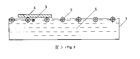
In fig. 3, the lower surface of the semiconductor substrate 4 is at a short
distance of about 2
mm from the liquid surface of the chemical solution 5. While the roller shaft
2 continues to move
the semiconductor substrate 4 horizontally, chemical solution 5 is gradually
in contact with and
wets the other parts of the lower surface of the semiconductor substrate 4 due
to surface tension
effect. Here, the nozzle 3 may be in a state of jetting the chemical solution
5 continuously or in a
state of stopping jetting. In the case of when the nozzle 3 is in the state of
jetting the chemical
solution 5 continuously, it may be in a state of moving either in a reverse
direction to
semiconductor substrate 4, or in a same direction but with a slower speed than
the semiconductor
substrate 4.
In fig. 4, the lower surface of the semiconductor substrate 4 is at a short
distance of about 2
mm from the liquid surface of the chemical solution 5. The roller shaft 2
continues to move the
semiconductor substrate 4 horizontally over the nozzle 3. Then the nozzle 3
stops jetting the
chemical solution 5. The lower surface of the semiconductor substrate 4 is
wetted completely by
the chemical solution 5 and in contact with the liquid surface.
In fig. 5, the lower surface of the semiconductor substrate 4 is at a long
distance of about 3
mm from the liquid surface of the chemical solution 5. When the roller shaft 2
moves the
semiconductor substrate 4 horizontally to above the nozzle 3, the nozzle 3
begins to jet the
chemical solution 5. Since the lower surface of the semiconductor substrate 4
is at a long
I t
CA 02693135 2010-01-15
distance from the liquid surface of the chemical solution 5, the chemical
solution 5 can not be in
contact with the lower surface of the semiconductor substrate 4 by means of
surface tension
effect. So the nozzle 3 jets the chemical solution 5 continuously during the
movement of the
semiconductor substrate 4 above the nozzle 3. When the semiconductor substrate
4 moves away
from the above of the nozzle 3, its lower surface is wetted completely but not
in contact with the
liquid surface. The semiconductor substrate 4 moves forward continuously and
may be processed
again by the next nozzle 3. Also, the chemical solutions jetted by different
nozzles 3 may be
same or different, which depends on the actual requirement.
Example 1
The chemical solution was a mixing solution of nitric acid and hydrofluoric
acid. The jet
apparatus was consisted of one nozzle and fixed. The lower surface of the
semiconductor
substrate is 2 mm above the liquid surface of the chemical solution. When one
end of the
semiconductor substrate moved to the above of the nozzle, the nozzle jetted
the chemical
solution one time. Then with the movement of the semiconductor substrate, its
lower surface was
wetted gradually by the chemical solution due to surface tension effect.
During the whole
processing, the lower surface of the semiconductor substrate kept in contact
with the liquid
surface of the chemical solution contained in the chemical tank. After the
processing, it showed
that the upper surface of the semiconductor surface was not wetted by the
chemical solution.
Example 2
The jet apparatus was consisted of several nozzles and fixed. The lower
surface of the
semiconductor substrate is 10 mm above the liquid surface of the chemical
solution. When one
end of the semiconductor substrate moved to the above of the nozzle, the
nozzle began to jet the
solution of hydrofluoric acid and continued until the other end of the
semiconductor substrate
moved to the above of the nozzle. Then the semiconductor substrate continued
to move, and
when one end of the semiconductor substrate moved to the above of the next
nozzle, the nozzle
began to jet the solution of hydrofluoric acid and continued until the other
end of the
semiconductor substrate moved to the above of the next nozzle. During the
whole processing, the
lower surface of the semiconductor substrate was not in contact with the
liquid surface of the
chemical solution contained in the chemical tank. After the processing, it
showed that the upper
surface of the semiconductor surface was not wetted by the chemical solution.
12
CA 02693135 2010-01-15
Example 3
The chemical solution was a chemical nickelizing solution. The jet apparatus
was consisted
of one nozzle and fixed. The lower surface of the semiconductor substrate is
0.1 mm above the
liquid surface of the chemical solution. When one end of the semiconductor
substrate moved to
the above of the nozzle, the nozzle began to jet the chemical nickelizing
solution and continued
until the other end of the semiconductor substrate moved to the above of the
nozzle. During the
whole processing, the lower surface of the semiconductor substrate kept in
contact with the
liquid surface of the chemical solution contained in the chemical tank. After
the processing, it
showed that the upper surface of the semiconductor surface was not wetted by
the chemical
solution.
Example 4
The chemical solution was an isopropanol solution. The jet apparatus was
consisted of
several nozzles and fixed. The lower surface of the semiconductor substrate
was 5 mm above the
liquid surface of the chemical solution. When one end of the semiconductor
substrate moved to
the above of the nozzle, the nozzle began to jet the isopropanol solution and
continued until the
other end of the semiconductor substrate moved to the above of the nozzle.
Then the
semiconductor substrate continued to move, and when one end of the
semiconductor substrate
moved to the above of the next nozzle, the next nozzle began to jet the
solution of hydrofluoric
acid and continued until the other end of the semiconductor substrate moved to
the above of the
next nozzle. During the whole processing, the lower surface of the
semiconductor substrate was
not in contact with the liquid surface of the chemical solution contained in
the chemical tank.
After the processing, it showed that the upper surface of the semiconductor
surface was not
wetted by the chemical solution.
The processing method and device thereof according to the present invention
are not only
suitable for processing a certain surface of the semiconductor substrate. It
is apparent for the
person skilled in the art to make various improvements or modifications
without departing from
the spirit and scope of the present invention. Therefore, the application of
the processing method
and device thereof according to the present invention in processing a single
surface of other
objects will also fall in the protective scope of the present invention.
13