Note : Les descriptions sont présentées dans la langue officielle dans laquelle elles ont été soumises.
CA 02693737 2010-02-19
PATENT APPLICATION
INVERTER FOR A DISTRIBUTED POWER GENERATOR
Related Applications
This application claims the benefit of the filing date of United States
Provisional Patent
Application No. 61/202,355, filed on February 20, 2009, the contents of which
are incorporated
herein by reference in their entirety.
Field of the Invention
This invention relates to circuits, systems, and methods for obtaining power
from a
distributed power generator such as a photovoltaic cell, and for interfacing a
distributed power
generator to a power distribution grid. In particular, this invention relates
to a maximum power
point tracker and a string/multi-string photovoltaic cell inverter
incorporating the maximum
power point tracker.
Background of the Invention
Grid-connected distributed power generators such as photovoltaic (PV) systems
typically
consist of two major parts: PV cell arrays to convert irradiation to
electrical energy, and an
inverter to feed the electrical energy into a power distribution grid. PV cell
configurations may
be categorized according to four groups [I]: centralized, string, multi-
string, and AC-module and
AC-cell technologies, see Figure 1(a). All approaches have advantages and
disadvantages [1],
[2], and compromise various attributes such as harmonic rejection capability,
simplicity,
efficiency, flexibility, reliability, safety, modularity, and cost.
The centralized topology is considered the best for high power applications
because the
input power level can be increased, and it uses only one inverter which
increases the conversion
efficiency. However, this topology has limitations. For example, since there
is significant high
voltage DC wiring between the PV cells and the inverter, the topology requires
expensive DC
-1-
CA 02693737 2010-02-19
PATENT APPLICATION
switches and special isolation, safety, and protection circuits. Due to the
centralized maximum
power point tracking (MPPT), partial shading of the PV cells or any mismatch
between the PV
cells causes a significant drop in the output power generation.
For medium power applications, the most suitable configuration is considered
to be the
string or multi-string technologies, [3], where one or more strings of PV
cells are connected to a
single inverter, as shown in Figure 1(b). Unlike the centralized
configuration, this type of
configuration enables independent MPPT for all strings which might be
installed in different
sizes and orientations. This also increases the overall efficiency under
certain circumstances,
such as partial shadowing of the PV cells. Therefore, this topology offers the
flexibility to
optimize the number of strings and inverters for the specific application
power level to increase
the overall efficiency and to reduce losses.
Since the PV cell array current-voltage characteristic is highly nonlinear,
the MPPT of
PV cell arrays is challenging. MPPT systems usually consist of two parts; MPP
tracker
hardware, and an algorithm. The MPP tracker alters the input resistance of the
inverter seen
from the output terminal of the PV cells that results in a change of the
operating point. MPPT
algorithms [4] calculate the best operating point available based on the
current irradiation and
temperature of the PV cells and provide a reference point for the MPP tracker
hardware.
In single-phase or unbalanced three phase grid-connected systems, the
instantaneous
power injected to the grid oscillates at twice the grid frequency. One of the
MPP tracker tasks is
to decouple the power oscillation from the PV cells, because the oscillation
results in a deviation
from the optimum operating point of the PV cells [2], [5]. This problem is
usually resolved by
connecting a large electrolytic capacitor at the PV cell terminals, which in
turn decreases the
lifetime and increases the volume, weight, and cost of the inverter. To avoid
the electrolytic
capacitor, an auxiliary circuit may be used [6], [7] which draws constant
current from the input
and generates a high DC voltage at the middle stage to supply the pulsation
required at the
output. In [8], an auxiliary circuit was proposed with a transformer and
passive and active
components to avoid oscillation. However, such solutions have low efficiency
and have
complex hardware and control systems, which make the overall system expensive.
-2-
CA 02693737 2010-02-19
PATENT APPLICATION
Summary of the Invention
Described herein is a maximum power point (MPP) tracker topology which
decouples
output power oscillations from the PV cell power generation. The topology may
extract the
maximum available power from each PV cell string of a multi-string system
independently. The
circuit uses a minimum number of components and avoids the use of large
electrolytic
capacitors, which is a major factor in limiting circuit life time. The MPP
tracker is not limited to
low-power applications. Such decoupling, described herein, is applicable to
voltage source
converter topologies and current source converter topologies.
One embodiment provides a maximum power point (MPP) tracker for a photovoltaic
cell,
comprising: high side and low side input points for the photovoltaic cell; a
capacitor connected
across the high side and low side input points; a switch connected between the
high side input
point and a node; an inductor connected between the node and a high side
output point; a
unidirectional conducting device connected between the node and the low side;
a low side output
point; and a maximum power point (MPP) tracker controller; wherein the switch
controls the
voltage across the capacitor. The capacitor voltage may be controlled between
a lower limit and
an upper limit.
Another embodiment provides a maximum power point (MPP) tracker for a
photovoltaic
cell, comprising: high side and low side input points for the photovoltaic
cell; a series input
inductor connected to the high side input point; a switch connected between
the series input
inductor and a node; an output inductor connected between the node and a high
side output point;
a unidirectional conducting device connected between the node and the low
side; a low side
output point; and a maximum power point (MPP) tracker controller; wherein the
switch controls
the current through the inductor. The inductor current may be controlled
between a lower limit
and an upper limit.
Also described herein is a PV cell inverter using a current source (e.g., buck-
boost)
topology in which the output voltage may be greater or smaller than the
voltage of the input PV
cell. Unlike voltage source topologies, the inverter directly generates and
feeds the desired
current into the grid using a modified pulse width modulation (PWM) technique.
The modified
PWM technique and control strategy optimize the middle stage dc current level
in the inverter.
-3-
CA 02693737 2010-02-19
PATENT APPLICATION
This results in a flatter efficiency curve for a wide range of input power.
The PV cell may
comprise a string of multiple PV cells, or multiple strings of PV cells.
Also described herein is an inverter for a photovoltaic cell, comprising: an
MPP tracker
as described above; and a means for generating a sinusoidal output current
from the MPP tracker
output.
The means for generating a sinusoidal output current may comprise a current
source
inverter or a voltage source inverter.. In one embodiment, the means for
generating a sinusoidal
output current may comprise a pulse width modulator. The means for generating
a sinusoidal
output current may comprise a means that modifies a pulse width modulation
reference signal to
cancel harmonics in an output current of the inverter. The means that modifies
a pulse width
modulation reference signal may comprise a PI controller and a compensator.
Also described herein is a method of applying a maximum power point tracker to
a
photovoltaic cell, comprising: connecting the output voltage of the
photovoltaic cell across a
capacitor; maintaining voltage across the capacitor between a lower limit and
an upper limit to
produce output power; wherein the upper limit is a reference voltage; wherein
the lower limit is a
function of a selected switching frequency of a switching circuit and an
output current of the
photovoltaic cell; wherein the output power is the maximum power available
from the
photovoltaic cell at a given instant in time.
The method may comprise connecting the output voltage of a string of two or
more
photovoltaic cells across the capacitor. The method may comprise using a
switching circuit to
maintain the voltage across the capacitor.
Another aspect relates to a method for obtaining power from a photovoltaic
cell,
comprising: using the maximum power point tracker with the photovoltaic cell
and producing
output power according to the method described above; and generating a
sinusoidal output
current from the output power.
The method may comprise using pulse width modulation (PWM) to generate the
sinusoidal output voltage or current. The method may comprise using pulse
width modulation to
cancel a harmonic in the output voltage or current. Generating a sinusoidal
output current may
comprise using a current source inverter or a voltage source inverter. The
method may comprise
-4-
CA 02693737 2010-02-19
PATENT APPLICATION
connecting the sinusoidal output current to a power distribution grid. The
method may comprise
connecting the output voltage of a string of two or more photovoltaic cells
across the capacitor.
Another aspect relates to a method for obtaining power from a plurality of
photovoltaic
cells, comprising: tracking the maximum power point of each photovoltaic cell
and producing
output power from each photovoltaic cell using the method described above; and
generating a
sinusoidal output current from the output power.
Also described herein is a method for obtaining power from a plurality of
photovoltaic
cells, comprising: using a maximum power point tracker with each string of
photovoltaic cells or
modules and producing output power from each string of photovoltaic cells or
modules
according to the method of described above; and generating a sinusoidal output
current from the
output power.
Also described herein is a method of cancelling a harmonic in an output
voltage or
current of a circuit, comprising using a PWM technique. Using a PWM technique
may comprise
using a modified PWM technique. The modified PWM technique may comprise
modifying a
PWM reference signal to increase or decrease output current and power of the
circuit. The
harmonic may be related to an oscillation of an input voltage or current of
the circuit. The circuit
may be a current source inverter or a voltage source inverter.
Also described herein is a PV cell system for connecting PV cells to a power
distribution
grid, comprising a PV cell inverter as described herein and one or more PV
cells.
The topologies described herein accept low PV cell voltages at the input,
which increases
efficiency in partial shading conditions, compared to topologies in which many
PV cells are
connected in series to build up a high input voltage.
Also described herein is a circuit for use with a distributed power generator,
comprising:
a high side input point and a low side input point for the distributed power
generator; a high side
output point and a low side output point; and (i) a parallel input capacitor;
and a means that
regulates voltage across the capacitor; wherein regulating voltage across the
capacitor
substantially removes distributed power generator input voltage oscillation;
or (ii) a series input
inductor; and a means that regulates current through the series input
inductor; wherein regulating
-5-
CA 02693737 2010-02-19
PATENT APPLICATION
current through the series input inductor substantially removes distributed
power generator input
current oscillation.
The voltage across the capacitor may be regulated between a lower limit and an
upper
limit. The means that regulates voltage across the capacitor may comprise a
switch connected
between the high side input point and a node; an output inductor connected
between the node and
the high side output point; and a diode connected between the node and the low
side output
point. The upper limit may be a reference voltage and the lower limit may be
calculated so that a
switching frequency of the switch and the distributed power generator input
voltage oscillation
or input current oscillation do not exceed selected values. The reference
voltage may be
obtained from a maximum power point tracking (MPPT) algorithm. The circuit may
include a
controller for the switch. The controller may be a hysteresis controller.
The current through the series input inductor may be regulated between a lower
limit and
an upper limit. The means that regulates current through the series input
inductor may comprise:
a switch connected between the series input inductor output and the low side
input point; and a
diode connected in series between the series input inductor and the high side
output point. The
upper limit may be a reference current and the lower limit may be calculated
so that a switching
frequency of the switch and the distributed power generator input current
oscillation do not
exceed selected values. The reference current may be obtained from a maximum
power point
tracking (MPPT) algorithm. The circuit may include a controller for the
switch. The controller
may be a hysteresis controller.
Also described herein is an inverter for a distributed power generator,
comprising: the
circuit described above; and a means that generates a sinusoidal output
current from the circuit
output. In one embodiment of the inverter, (i) the circuit includes a parallel
input capacitor and a
means that regulates voltage across the capacitor, and the inverter comprises
a current source
inverter; or (ii) the circuit includes a series input inductor and a means
that regulates current
through the series input inductor, and the inverter comprises a voltage source
inverter.
Also described herein is a compensator for use with a voltage source inverter
or a current
source inverter, wherein the compensator modifies a pulse width modulation
(PWM) reference
-6-
CA 02693737 2010-02-19
PATENT APPLICATION
signal of the voltage source inverter or current source inverter, to cancel
one or more harmonic in
the voltage source inverter or current source inverter output current.
Also described herein is an inverter as described above, including a
compensator,
wherein the compensator modifies a pulse width modulation (PWM) reference
signal of the
voltage source inverter or the current source inverter, to cancel one or more
harmonic in the
voltage source inverter or current source inverter output current.
Also described herein is a method for obtaining power from a distributed power
generator, comprising: (i) connecting a capacitor across the output voltage of
the distributed
power generator; and actively regulating voltage across the capacitor; wherein
regulating voltage
across the capacitor substantially removes distributed power generator voltage
oscillation; or (ii)
connecting a series input inductor to the output of the distributed power
generator; and actively
regulating current through the inductor; wherein regulating current through
the inductor
substantially removes distributed power generator current oscillation.
The method may comprise: (i) using a switch to regulate the voltage across the
capacitor;
or (ii) using a switch to regulate the current through the inductor. The
method may include
regulating the voltage across the capacitor between an upper limit and a lower
limit. The upper
limit may be a reference voltage and the lower limit may be calculated so that
a switching
frequency of the switch and the distributed power generator input voltage
oscillation or input
current oscillation do not exceed selected values. The method may include
using hysteresis to
control the switch.
Also described herein is a method for obtaining power from a distributed power
generator
and producing a sinusoidal output current, comprising: (i) connecting a
capacitor across the
output voltage of the distributed power generator; actively regulating voltage
across the capacitor
to substantially remove distributed power generator voltage oscillation; and
using a current
source inverter to produce the sinusoidal output current; or (ii) connecting a
series input inductor
to the output of the distributed power generator; actively regulating current
through the inductor
to substantially remove distributed power generator current oscillation; and
using a voltage
source inverter to produce the sinusoidal output current.
-7-
CA 02693737 2010-02-19
PATENT APPLICATION
The method may further comprise connecting the sinusoidal output voltage or
current to a
power distribution grid.
Also described herein is a method of obtaining power from voltage source
inverter or a
current source inverter, comprising modifying a pulse width modulation (PWM)
reference signal
of the voltage source inverter or current source inverter to cancel one or
more harmonic in the
voltage source inverter or current source inverter output current. The method
may further
comprising modifying a pulse width modulation (PWM) reference signal of the
voltage source
inverter or current source inverter to cancel one or more harmonic in the
voltage source inverter
or current source inverter output current.
In the above embodiments, the distributed power generator may be a wind
turbine or a
photovoltaic cell.
Brief Description of the Drawings
For a better understanding of the invention, and to show more clearly how it
may be
carried into effect, embodiments will now be described, by way of example,
with reference to the
accompanying drawings, wherein:
Figure IA shows a block diagram of PV cell systems categorized by different PV
cell
configurations and inverter types, according to the prior art.
Figure 1 B shows a block diagram of a multi-string PV cell inverter
configuration,
according to the prior art.
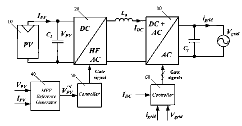
Figure 2 is a generalized block diagram of a PV cell inverter according to an
aspect of the
invention.
Figure 3A is a schematic diagram of a maximum power point tracker circuit and
a
controller according to one embodiment. The inset plot of Vp,, as a function
of time shows
operation of the main switch SB according to one embodiment.
-8-
CA 02693737 2010-02-19
PATENT APPLICATION
Figure 3B is a schematic diagram of a maximum power point tracker circuit and
a
controller according to another embodiment. The inset plot of Ip, as a
function of time shows
operation of the main switch SB according to the embodiment.
Figure 3C shows only the ripple of the PV cell voltage, power, and current
waveforms
during three switching cycles of the embodiment of Figure 3A.
Figures 4A and 4B show voltage and current waveforms for the inductor LB in
the
embodiment of Figure 3A.
Figure 5A is a schematic diagram of a single-string grid-connected PV cell
inverter
according to one embodiment.
Figure 5B is a schematic diagram of a multi-string grid-connected PV cell
inverter based
on the single-string embodiment of Figure 5A.
Figure 6 shows an embodiment of a modified pulse width modulation technique
used in
the controller for the current source inverter of the embodiment shown in
Figure 5A or 5B.
Figure 7 is a block diagram of a control scheme for a single-string inverter
according to
one embodiment, showing control of the modified pulse width modulation
technique of Figure 6.
Figure 8 is a block diagram of a control scheme for a multi-string inverter
based on the
embodiment of Figure 7.
Figure 9 is a plot showing output grid current with no harmonic cancellation
and a 120
Hz harmonic, then harmonic cancellation, and finally with a low inductor
current reference.
Figure 10 is a plot showing results of a simulation of the embodiments shown
in Figures
5B and 8, under various conditions of irradiance level, input voltage, and
partial shading of the
PV cells.
-9-
CA 02693737 2010-02-19
PATENT APPLICATION
Detailed Description of Embodiments
Described herein are systems, circuits, and methods for obtaining power from a
distributed power generator, the obtained power being suitable for injection
into a power
distribution grid. A distributed power generator may be, for example, a wind
turbine or a
photovoltaic cell. Whereas embodiments of the systems, circuits, and methods
are described
herein primarily with respect to photovoltaic cells, it will be appreciated
that the systems,
circuits, and methods are limited thereto.
For example, described herein is an inverter for obtaining power from one or
more
photovoltaic cells. In one embodiment, the inverter is for interfacing one or
more PV cells to a
power distribution grid. Such an embodiment is shown in Figure 2. This
embodiment includes
an input capacitor C1 connected across the PV cell(s) 10, a first stage
including an MPP tracker
circuit 20 connected across the input capacitor, and a series inductor LB
connected to the MPP
tracker output, and a second stage including an output inverter, and an output
capacitor CAC. The
first stage also includes a controller 50 for the MPP tracker circuit 20, and
a circuit 40 to
generate a reference voltage. With the controller 20, the MPP tracker circuit
20 controls the
voltage across the input capacitor C1. The second stage also includes a
controller 60 for the
inverter 30.
Features of the PV inverter embodiments described herein include: a low PV
cell voltage
is accepted, which improves efficiency at partial shading conditions of the PV
cells; a wide range
of input voltage is accepted; adaptive control of the inductor LB current DC
level optimizes the
modulation index for the inverter over a wide range of input power levels;
input and output
power decoupling are provided with,only a small input capacitor C1i a fast MPP
tracker; and
integration of the MPP tracker into a PV cell array is possible because no
passive component is
required for the input of the MPP tracker stage. These features will be
described in detail below.
As used herein, the terms "maximum power point tracking (MPPT)" and "maximum
power point tracker (MPP tracker)" are distinct. "MPPT" refers to an algorithm
and "MPP
tracker" refers to hardware (i.e., a circuit). The MPPT calculates the optimum
operating point
for a distributed power generator such as a photovoltaic cell, and provides a
reference point for
MPP tracker to steer the system toward the optimum operating point.
-10-
CA 02693737 2010-02-19
PATENT APPLICATION
As used herein, the term "photovoltaic cell" refers to any cell having a light
absorbing
material to absorb photons and generate electrons via a photoelectric effect.
A non-limiting
example of a photovoltaic cell is a solar cell. The light absorbing material
may absorb light in
any wavelength or combination of wavelengths, including, for example,
wavelengths of solar
light that reach the earth's surface, and/or wavelengths of solar light beyond
the earth's
atmosphere. Two or more light absorbing materials having specific wavelengths
of light
absorption may be used in combination to take advantage of different light
absorption and charge
separation mechanisms. The light absorbing material may be configured as, for
example, bulk
material, thin-film (e.g., inorganic layers, organic dyes, and organic
polymers), and/or
nanocrystals. The photovoltaic cells may be combined into arrays, strings, or
panels.
As used herein, the term "photovoltaic cell string" refers to a plurality of
photovoltaic
cells connected together in a series, parallel, series-parallel, or other
configuration.
Power Decoupling
The instantaneous output power oscillates at twice the grid frequency in
single-phase
grid-connected systems. In PV systems, the input power generation is dc and
thus the oscillation
of the instantaneous output power, if reflected in the input, causes the input
operating point to
deviate from dc. If there is power oscillation on the PV side, maximum power
is only achievable
at the peak of oscillation, which translates into less average power
extraction than the available
maximum power. This is a power loss that reduces the efficiency of the PV
system.
Substantially the same problem exists in systems with wind turbines or fuel
cells at the input for
single phase systems or unbalanced three phase systems. Therefore, power
oscillation is a key
problem in such systems and the converter should decouple the output power
oscillation from the
input dc power generation to maximize efficiency. Power decoupling is
conventionally
performed by using large electrolytic capacitors in the design to minimize the
effect of the output
power oscillation on the input operating point. However, use of large
capacitors lowers the
reliability of the hardware, resulting in high maintenance expenses.
Conventional approaches use a control system to regulate the average of the
input voltage
or current to achieve maximum power point tracking and to reach sufficient
amplification gain.
-I1-
CA 02693737 2010-02-19
PATENT APPLICATION
In such approaches decoupling is accomplished by either passive elements or
auxiliary power
circuits.
In contrast, the maximum power point tracker described herein forces the input
voltage or
current to track a reference signal very tightly. As a result, the double
frequency oscillation is
displaced and the input power generation is at or very close to the optimum dc
level.
Power decoupling as described herein may be implemented using a closed loop
control
system with high bandwidth, such as, for example, a hysteresis controller, or
an open loop
control system having high gain at the frequency of the oscillatory harmonic.
That is, although
the operating point of the converter oscillates at twice the grid frequency,
the converter should
respond with sufficient speed to reject the effect of this distortion from the
power generation
(e.g., PV) side.
The high open loop gain or closed loop bandwidth of the system will eventually
cause
very low or zero steady state error with fast tracking of the input reference
point. As a result,
input power decoupling is accomplished only by means of the control strategy
and/or the high
switching frequency, rather than methods that use bulky passive elements or
auxiliary circuits.
For example, a high switching frequency converter at the PV side as described
herein can
remove the oscillatory harmonics at the input. Power decoupling may also be
accomplished
using a resonant controller tuned at the oscillatory harmonic to generate high
open loop gain at
the PV side converter.
MPP Tracker
Figure 3A is a schematic diagram of an MPP tracker circuit 20, and its
controller 50 and
reference voltage circuit 40, according to one embodiment. The inset plot of
V.,, as a function of
time shows an embodiment of a control strategy for this circuit. Other control
strategies may
also be used. In the embodiment shown in Figure 3A, the MPP tracker circuit
includes a series
switch SB connected to the high side input terminal and a unidirectional
conducting device such
as a diode DB connected between the switch output and the low side input
terminal. In operation,
the main switch SB is used to regulate the input capacitor CI voltage.
Regulating the input
-12-
CA 02693737 2010-02-19
PATENT APPLICATION
voltage enables the inverter to displace output power oscillation from the
input terminal,
substantially removing PV cell voltage oscillation and avoiding the need for
large input
capacitors at the PV terminals. Removal of the input voltage oscillation
stabilizes the input
operating point, resulting in high efficiency conversion with much smaller
capacitors.
Figure 3B is a schematic diagram of an MPP tracker circuit 20, and its
controller 50 and
reference voltage circuit 40, according to another embodiment. The inset plot
of Ip,, as a function
of time shows an embodiment of a control strategy for this circuit. Other
control strategies may
also be used. In the embodiment shown in Figure 3B, the MPP tracker circuit
includes a series
input inductor L.,,, a switch SB, and a unidirectional conducting device such
as a diode D
connected in series with the high side output terminal. In operation, the main
switch SB is used
to regulate the current through the inductor Lp,,. Regulating the inductor
current enables the
inverter to displace output power oscillation from the input terminal,
substantially removing PV
cell voltage oscillation and avoiding the need for large input capacitors at
the PV terminals.
Removal of the input current oscillation stabilizes the input operating point,
resulting in high
efficiency conversion with much smaller capacitors.
Figure 3C shows the ripple of the input voltage, power, and current waveforms
from the
PV cells, for the embodiment of Figure 3A. A typical PV cell i-v
characteristic curve includes
three operating conditions: 1) operation at a voltage lower than the optimum
point where the PV
cell voltage is increased and the power is increased; 2) operation at a
voltage higher than the
optimum point where the PV cell voltage is increased and the power is
decreased; and 3)
operation around the optimum point where the PV voltage is increased and the
power is
maximum, where the MPP is tracked. It is clear from Figure 3B that the MPP is
tracked since
during the rise time of the PV cell voltage, the output power reaches its
maximum. The control
strategy of the above MPP tracker embodiment may accept a reference voltage
from any MPP
tracking algorithm (such as, for example, a perturb/observe algorithm), to
obtain the maximum
power available from the PV cells independent of the output voltage and
current. The power is
delivered to the inverter stage 30 and, as described below, the output current
and voltage of the
MPP tracker are controlled and induced by the inverter stage. This topology
may provide power
to any load or inverter configuration (e.g., voltage source inverter, current
source inverter) at the
next stage.
-13-
CA 02693737 2010-02-19
r PATENT APPLICATION
As shown in Figure 4A, the output of the switch SB is a high frequency
oscillating voltage
VD. However, the input of the inverter 30 is a low frequency (e.g., twice the
grid frequency, 120
Hz) oscillating voltage V,,,,,. The current in the inductor LB includes dc, an
oscillating current at
twice the grid frequency, and high frequency harmonics. Therefore, as shown in
Figure 4B, the
inductor current includes a double grid frequency harmonic that should not be
injected to the
output grid current. In one embodiment, described below, the double grid
frequency harmonic is
removed using a modified pulse width modulation (PWM) strategy.
Control Strategy for MPP Tracker
An embodiment of the input capacitor C1 voltage control may be briefly
described as
follows. The capacitor voltage Vpv is maintained between two upper and lower
levels. This is
done by the hysteresis control strategy as shown in Figure 3A. The controller
may be
implemented with two comparators and two comparison levels. The upper level,
V"f, may be
obtained from an MPPT algorithm. The lower level, Vpv - AVp,,, is not constant
and is
calculated in such a way that for all conditions, the switching frequency and
the voltage ripple do
not exceed selected values. This will be shown below. When the input capacitor
voltage Vpv
exceeds the upper level, the output of the upper comparator becomes high, the
flip-flop is set,
which turns the main switch SB on, and discharges the capacitor. The switch
remains on until the
flip-flop is reset when the capacitor voltage hits the lower limit.
In summary, the controller maintains the PV cell voltage very close to the
optimum
reference point provided by the MPPT algorithm. Since the level of the input
voltage is
proportional to the power generation, by controlling the input voltage the
power fed to the circuit
is controlled and this stage becomes a controllable power source. For example,
if the output of
this stage was connected to a heater (e.g., a resistor), the heat transfer
would be linearly
controlled by the input reference voltage.
The capacitor value and A Vpv may be selected such that the operating
frequency of the
circuit is always less than a certain limit and the voltage ripple is less
than %8.5Vp P" in order to
reach a utilization ratio higher than %98. Any ripple at the PV cell voltage
decreases the
-14-
I I CA 02693737 2010-02-19
PATENT APPLICATION
efficiency (or utilization ratio), because the maximum power is extracted when
the voltage is
equal to Vp "P, and any deviation due to the voltage ripple decreases the
output power.
During the time that the switch SB is off the following relationship is valid:
Cif ,f f (1)
To limit the switching frequency, f is restricted because f S < f. The
equation
toff4. ton
above shows that f = ciovp,,. By substitution it can be shown that if AV, is
chosen as Cif,, for
all conditions the time off will be almost constant because toff = f = f" `,
where f'r` is the
maximum frequency.
The voltage of the PV cells is minimized, i.e., V n , at the lowest operating
temperature.
As mentioned above, it is desired that 0 Vp,, < %8.5VjjPP. Therefore, this
inequality holds true
for all conditions if AVpõ < %8.5V,miPn .
From (1) and the above inequality it can be shown that ifd < %8.5VMzn". For
this
inequality to be true for all conditions, the left hand side is maximized to
calculate the capacitor
value. The maximum value of the PV cells iM.PP is known and occurs at full
irradiation. As a
result, the input capacitor Cl value may be determined as:
1MFP
9'8 .51 1P fri-
It is clear from the above equation for C1 that in obtaining a desired PV
voltage variation,
there is a trade-off between the switching frequency and the capacitor value.
If the parameters
are chosen in this way, this control scheme provides that for all irradiation
and temperature levels
the circuit operates below the selected desired frequency and the above %98
utilization ratio.
For example, if ip" = 4A, V " = 1.00 V, and f m = 20 KHz, the capacitor will
be C1= 20 F ,
where the PV cell voltage variation is selected to be LVp,, = 5V.
-15-
CA 02693737 2010-02-19
PATENT APPLICATION
Current Source PV cell Inverter
Figure 5A is a circuit diagram of a single-string PV cell inverter according
to one
embodiment. Shown is the PV cell string 10, the MPP tracker 20, a current
source inverter 30,
and a low pass filter 70 including Cf and Lf to eliminate output current high
frequency
components. The low pass filter 70 may be replaced by higher order filters for
a further
reduction in the size of the passive components.
Figure 5B shows a circuit diagram of a multi-string PV cell inverter according
to another
embodiment. This embodiment is based on the circuit of Figure 5A, but includes
two MPP
tracker power circuits, and two strings of PV cell modules. However, any
number of power
circuits and PV cell strings may be used. In the first stage the MPP trackers
are connected in
parallel, and each MPP tracker is connected to a PV cell string. The second
stage includes a
current source inverter, which is connected to the distribution grid. With
this embodiment of the
control algorithm a voltage source inverter may be used instead of the current
source inverter, if
a small capacitor is used at the input of the voltage source inverter.
In one embodiment, the controller for the current source inverter uses a PWM
scheme.
To understand the principle of operation, first assume that the current source
inverter is fed by a
dc current source and the PWM scheme modulates a sinusoidal reference waveform
to generate a
sinusoidal output current, as shown in Figure 6. As a result of the PWM
strategy the voltage
induced at the input of the current source inverter is the modulated grid
voltage, full-wave
rectified, V;,,, as shown in Figure 4A. However, the input of the current
source inverter stage is
connected to the MPP tracker output, which is not a constant current source.
Thus, the input
current of the current source inverter, changes according to the induced
voltage as discussed
above. Oscillation induced in the inductor current is inevitable because the
input power
generation is kept constant by the MPP tracker circuit, but the output power
oscillates at twice
the grid frequency and thus, the power oscillation has to be supplied from an
energy storage
component, such as the inductors of the MPP tracker circuits. Therefore, the
PWM technique
may be modified to generate a pure sinusoidal waveform based on the
oscillatory input current
source. In one embodiment, shown in Figure 6, this is accomplished by
formulating the inductor
current, and then modifying the reference signal to the PWM modulator so that
it regulates and
-16-
CA 02693737 2010-02-19
PATENT APPLICATION
controls the dc component of the inductor current iL, and prevents the double
frequency harmonic
component of iL from appearing in the output ac current.
Inductor DC Current Regulation
Inductor current regulation will now be described with respect to PV string #I
of Figure
5B. Assume that the converter is lossless (Pin = Pogo) and the output filter
energy storage is
negligible. Also, assume that there is only one PV cell string (string #1)
connected to the circuit.
Therefore, the only energy storage component is LA. As discussed above, the
MPP tracker
circuit extracts constant power from the PV cells. Assuming that the current
source inverter
generates a current in-phase with the grid voltage, the output power may be
derived as follows:
i,(t) = Ia sin(wt), v,o (t) _ Va sin(wt) =
1
Po(t) = 2 Vala(1 - cos(2wt))
1 ~ 1
w
Pin = pavo = 2-7c po(t)dt = VOIa (2)
0
At - 4 r' we have po(t) = Pin, and if ( w 1.U)s the input power will be
greater
than the output power. Therefore, for this time period the inductor LA will be
charged from
ILAmtn to ILA.:
1 2
~LAIIAMGX 1 A LAmin _ (in - pQ())
(3)
E I A = Pin ,ILA = ILAmin + ILATaz (4)
2wLATLA 2
Since the inductor current is equal to its dc value at t = 0, using a similar
procedure as
described above the inductor current as a function oft may be derived as
follows:
-17-
CA 02693737 2010-02-19
PATENT APPLICATION
iL A (t) _ , -{- 1 V'f,Io sin 2e . t (5)
2t~rLA
With reference to Figure 6, control of the inductor dc component using the
modulation
index of the PWM may be explained as follows. By reducing the modulation index
the output
current is reduced temporarily. Consequently, the output power decreases and
the difference
energy is stored in the inductor which in turn increases its dc value. As a
result, the output
current increases up to the point where the average power injected into the
grid equals the input
power.
To reduce the conduction losses and to obtain a flatter efficiency curve, the
inductor dc
current may be minimized by the modulation index for different input power
levels. Equations
(4) and (5) show that oscillation of the inductor current depends on the input
power, the inductor
value, and the inductor dc current. Thus, as the inductor dc current
decreases, AIL increases,
which eventually results in a discontinuous mode of operation where the output
current becomes
distorted.
To avoid this mode of operation, the minimum of the inductor current should be
higher
than the maximum output current when the second stage is, for example, a
voltage boost inverter
or a step down current source inverter. If a voltage source inverter is
utilized at the second stage
the oscillations will occur at the voltage of the inverter input capacitor. To
avoid a discontinuous
mode of operation the capacitor voltage should be larger than the grid
voltage, and a similar
approach may be used to derive equations for this mode of operation. Thus, the
following
inequality has to be satisfied:
ILA AIL Ia _ 2P* , (6)
i P- + art (' I
'Lac ? + V
V 2wL
a
The right hand side of the inequality forms the reference inductor current.
Figure 7
shows an example of the case when the reference current is too low and the
grid current is
-18-
CA 02693737 2010-02-19
PATENT APPLICATION
distorted (see Figure 9; low inductor, current reference). Since the minimum
possible inductor
current is desired, the equality may be used in the controller system to
generate a reference signal
for the inductor dc current, as shown in Figure 7, time interval (t1-t2).
Figure 7 shows a block diagram of an embodiment of the current source inverter
control
system, which consists of two parts: a proportional integral (PI) controller
100 to stabilize the
inductor dc current level and prevent discontinuous modes of operation; and a
compensator 200
that modifies the PWM reference signal to cancel harmonics at the grid
current. To form the
feedback loop, first the dc inductor value is measured and then the error
signal is fed into the PI
controller. The output of the PI controller adjusts the amplitude of the
output current reference
signal. When the error signal is positive, the inductor dc current is higher
than the reference and
has to be reduced. In this case the PI controller increases the reference PWM
signal and
consequently the output current and power increase. This, in turn, decreases
the inductor current
until the error signal is zero where the output of the PI controller remains
constant. The case
where the error signal is positive is similar. Since a PI controller is used,
the steady state error
will be zero and as a result, according to equation (7), the inductor current
is always minimized
to optimize conduction losses and also to ensure that the output current will
not become
discontinuous. When there is more than one PV cell string connected to the
circuit, the output
power equals the sum of the input powers. Thus, the output current may be
decomposed into
components corresponding to each string, for example, io(t) = iol(t) + io2(t).
However, the
charging and discharging of each inductor depends on the difference between
the power
generated by a string and the power injected to the system from that string.
Therefore, equations
(2),(4), and (5) hold true for any number of PV cell strings j, if i0, p,,,
P;,, and LA are substituted
by iol, poj , P,,, and Lx. If the inequality (6) is satisfied for each string
for any condition, the sum
of the inductors' currents will be larger than the maximum output current. The
reference current
for each string is calculated and added together to form one reference
inductor current and as a
result, the control strategy shown in Figure 7 regulates the do inductor
current of all strings. An
embodiment for a multi string inverter is shown in Figure 8.
A feature of this multi-string topology embodiment is that the output power
oscillation is
not supplied only by one inductor. Rather, all strings contribute to the power
oscillation. As a
result, with more strings, the current oscillation on each inductor is reduced
and smaller
-19-
CA 02693737 2010-02-19
PATENT APPLICATION
inductors may be used. Moreover, because of the smaller oscillations, equation
(5) results in a
smaller dc reference for the inductor currents, which in turn reduces the
conduction losses.
Harmonic Cancelation Method Using Modified PWM Technique
The embodiment described in the following section is based on a current source
inverter
(CSI). However, the method may be used to cancel an oscillation at the input
of other
converters, and in another embodiment a voltage source inverter (VSI) is used.
The below
description also applies to a voltage source inverter, the only difference
being that the input
source is voltage, the inductors are replaced by capacitors, and currents are
replaced with
voltages, and vice versa.
As shown in equation (5), the inductor current oscillates around a dc value at
twice the
grid frequency. Conventional sine PWM techniques assume a constant dc input
current, and thus
any harmonic of the input source will be reflected to the modulated output
current. This problem
may be avoided by introducing a compensation factor as shown in Figure 7. When
the
oscillatory current source inverter input do current increases, the
compensator decreases the
modulation index proportionally, which is done by the multiplication of the
signal labeled comp
(t) and the sine PWM reference signal as shown in Figure 7. As a result, an
increase in the dc
current value is compensated by a reduction in the modulation pulse width, and
vice versa. This
type of compensation prevents oscillatory harmonics from appearing at the
output current
because the PWM modulator creates the new sine PWM reference signal at the
output of the
inverter and thus the energy transfer to the output is equivalent to the case
where the inductor
current is a constant dc current with no oscillation. The modulation signals
and compensation
method are shown in detail in Figure 6. In Figure 6(a) two cases when the
inductor current is dc
or oscillatory are demonstrated. Figure 6(b) shows PWM reference and carrier
signals for the
above mentioned cases. As shown, the reference is modified by a factor which
shows how much
the inductor current has deviated from the do level. The effect of this
modification is shown in
Figure 6(b),(c) for the interval when the inductor current is higher than the
dc level. It can be
observed from waveform (d) that since the current is higher, the pulse width
is lower than the do
current and both waveforms transfer the same amount of energy to the output.
As a result, with
-20-
CA 02693737 2010-02-19
PATENT APPLICATION
this modification, the case where the inductor current is oscillatory, the
harmonics at the output
are similar to the case where the inductor current is pure dc. As explained
above this
modification may also be applied to the case where the second stage is a
voltage source inverter
and the input voltage is oscillatory.
The following non-limiting example is provided to further illustrate the
invention.
Example
To demonstrate the impact of the irradiance level, input voltage level, and
partial shading
on the performance of a two-string PV cell inverter as shown in Figures 5B and
8,, a simulation
was carried out using PSIM 7.0 software and the values set forth in Table I,
and the results are
shown in Figure 10. The system was started with string #2 partially shaded
(40% of the full
irradiation level) and string #1 at full power. At t = 0.2 (s) both strings
were partially shaded at
15% of the full irradiation level and the system response was obtained. At t =
0.3 (s) the
temperature of the PV cells was increased so that the output voltage of the PV
cells decreased
from 150V to 80V, which is less than the grid voltage. At t = 0.4 (s) both
strings were exposed
to full irradiance. It can be seen from Figure 10 that after each change, the
controller quickly
stabilized the output current. In addition, the maximum input power extraction
was almost
instantaneous, confirming the fast dynamic response of the MPP tracker
circuit. Overall, the
simulation results show that the converter is robust, and provides excellent
decoupling
performance for medium-power systems (such as residential applications).
-21-
CA 02693737 2010-02-19
PATENT APPLICATION
TABLE I
SIMULATION PARAMETERS
Parameters Values
CPV 1, CPV 2 20 p F
C 2 j.F
LA,LB 2000 IAH
.LLf 100011H
CSI f8 10 KHz
First age f na-T 20 KHz
Grid voltage 110 V
Grid frequency 60 Hz
PV String MPP 1.1KW
The contents of all references, pending patent applications, and published
patents cited
throughout this application are hereby expressly incorporated by reference.
Equivalents
Those skilled in the art will recognize or be able to ascertain variants of
the embodiments
described herein. Such variants are within the scope of the invention and are
covered by the
appended claims.
-22-
CA 02693737 2010-02-19
PATENT APPLICATION
References
[1] M. Meinhardt, G. Cramer, B. Burger, and P. Zacharias, "Multi-string
converter with reduced
specific costs and enhanced functionality," Solar Energy, vol. 69, no. 1, pp.
217-27, 2000.
[2] S. B. Kjaer, J. K. Pedersen, and F. Blaabjerg, "A review of single-phase
grid-connected
inverters for photovoltaic modules," IEEE Transactions on Industry
Applications, vol. 41, no. 5,
pp. 1292-1306, Sep./Oct. 2005.
[3] G. Walker and P. Sernia, "Cascaded DC/DC converter connection of
photovoltaic modules,"
IEEE Transactions on Power Electronics, vol. 19, pp. 1130-1139, 2004.
[4] T. Esram and P. L. Chapman, "Comparison of photovoltaic array maximum
power point
tracking techniques," IEEE Transaction on Energy Conversion, vol. 22, no. 2,
pp. 439-449, Jun.
2007.
[5] Y. Xue, L. Chang, S. B. Kjaer, J..Bordonau, and T. Shimizu, "Topologies of
single-phase
inverters for small distributed power generators: an overview," IEEE
Transactions on Power
Electronics, vol. 19, no. 5, pp. 1305-1314, Sep. 2004.
[6] T. Shimizu, K. Wada, and N. Nakamura, "A flyback-type single phase utility
interactive
inverter with low-frequency ripple current reduction on the DC input for an AC
photovoltaic
module system," Power Electronics Specialists Conference, pesc 02. IEEE 33rd
Annual, vol. 3,
pp. 1483- 1488, 2002.
[7] S. B. Kjaer and F. Blaabjerg, "Design optimization of a single phase
inverter for photovoltaic
applications," Power Electronics Specialist Conference, PESC '03. IEEE 34th
Annual, vol. 3, pp.
1183-1190, Jun. 2003.
[8] B. M. T. Ho and H. S.-H. Chung, "An integrated inverter with maximum power
tracking for
grid-connected PV systems," IEEE Transactions on Power Electronics, vol. 20,
no. 4, pp. 953-
962, Jul. 2005.
-23-