Note : Les descriptions sont présentées dans la langue officielle dans laquelle elles ont été soumises.
CA 02696066 2010-03-09
Doc No: 102-47 CA Patent
PHOTONIC FILTERING OF ELECTRICAL SIGNALS
TECHNICAL FIELD
The present invention relates to signal filtering, and in particular to
photonic filtering of
electrical signals.
BACKGROUND OF THE INVENTION
Communication satellites operating in the Ka-band frequency range often use a
large number of
microwave communication beams. The satellites typically have a lifetime of
over 15 years. It is
rather difficult to predict the information carrying capacity of individual
beams during such a
long period of time. Accordingly, dynamic allocation of the bandwidth among
the microwave
communication beams is highly desirable.
The dynamic bandwidth allocation can be provided by tunable microwave filters
having a
tunable central frequency and a variable width of the passband. Such tunable
microwave filters
can be installed in both the ground stations and onboard the satellites. To be
practically usable,
the tunable filters must possess a high stability of the spectral response,
strong out-of-band
rejection, and small group delay variation. Furthermore, tunable filters
placed on satellites must
be lightweight and meet stringent space-launch qualification requirements.
Electronic filters are ubiquitous in circuit design. Many types of electronic
filters are presently
available. The most common filters use bulk elements, such as capacitors,
inductors, and so on,
to form single- or multi-pole filters at appropriate frequencies of interest.
It is possible to build
tunable filters using switching banks or variable components. Although these
filters can operate
up to several gigahertz in frequency, they are mostly used for lower
frequencies, where the
physical dimensions of the components are still small compared to the
wavelength of operation.
Circuits operating at microwave frequencies typically use planar or coaxial
waveguide structures.
These filters utilize distributed capacitance and inductance created by a
particular geometry of
the waveguide structure, in conjunction with the abrupt variations in
impedance created by stubs
and slots, to form resonant cavities. Using ceramic materials or high-
temperature
superconductors to form very low loss substrates can result in very high
finesse (high-Q) filters.
1
CA 02696066 2010-03-09
Doc No: 102-47 CA Patent
Planar structures are reasonably easy to fabricate using conventional circuit
board techniques.
However, the circuit board based planar structures tend to be lossy at higher
frequencies due to
radiative loss. Coaxial structures are superior in this regard because the
outer conductor shields
the structure, but these tend to be bulky and heavy.
Millimeter-wave filters can be formed using dielectric resonators and cavity
structures, but they
are difficult to fabricate, and the resulting filter characteristics can be
very sensitive to
fabrication errors, particularly when the filters contain multiple coupled
resonators. Both the
microwave and the millimeter-wave filters are difficult to tune and have a
limited tuning range.
Furthermore, it is difficult to change the finesse of a particular filter or
to generate a variable
bandwidth filter.
In a satellite, a bank of filters is switched in and out of a signal path to
change the channel
bandwidth, and a programmable frequency converter is used to change the center
frequency.
There are two major difficulties associated with this approach. First, a very
limited number of
filters can be practically used due to a large number of communication beams,
and even these
few filters per beam result in a very heavy and bulky overall structure.
Second, once the set of
filters is determined, it remains fixed for the lifetime of the satellite.
Because of these intrinsic
difficulties, other approaches have been investigated.
One such approach, presented by Ming Yu et al. in a paper entitled "A Ka Band
Tunable Filter
for Reconfigurable Payload", 15th Ka and Broadband Communications, Navigation
and Earth
Observation Conference, Sept. 23-25, 2009, which is incorporated herein by
reference, consists
of having a mechanically tunable cavity filter. However, any mechanically
controlled devices or
subsystems in a satellite raise substantial reliability issues.
Another approach, exemplified in a paper by Glyn Thomas et al. entitled "Agile
Equipment for
an Advanced Ku/Ka Satellite", ESA Workshop on Advanced Flexible Telecom
Payloads, 18 - 20
November 2008, ESAIESTEC, Noordwijk, The Netherlands, which is incorporated
herein by
reference, uses an electrical heterodyne principle. The signal is frequency
down-converted to a
given intermediate frequency (IF) using a programmable synthesizer, two
cascaded bandpass
filters are used to achieve the required filtering, and then another
programmable synthesizer is
2
CA 02696066 2010-03-09
Doc No: 102-47 CA Patent
used to bring the signal to the desired channel frequency. The main drawbacks
of this circuit are
the power consumption, and large volume and mass, which are all very
detrimental for a space
application.
Electrical filters based on photonic circuits have been reported numerous
times, primarily in the
academic literature. These are generally based on: tapped delay lines to
emulate a finite impulse
response (FIR) filter, delay line interferometers, fiber Bragg grating (FBG)
delay lines,
dispersive fiber delays, and acousto-optic modulators. In general, these
techniques are better
suited towards forming notch filters, not bandpass filters required for a
satellite bandwidth
allocation and tuning applications.
Ilchenko et al. disclose in United States Patent Application US2005/0175358,
which is
incorporated herein by reference, a tunable radio frequency and microwave
photonic filter using
an optical heterodyne principle. Referring to FIG. 1, a filter 100 of Ilchenko
et al. is shown
having a laser 101, an electro-optical modulator (EOM) 102, a whispering-
gallery mode (WGM)
filter 103, a photodetector 104, beamsplitters 105, and mirrors 106. The WGM
filter 103 has
evanescent field couplers 107 and cascaded WGM resonators 108. In operation,
the laser 101
emits a beam at a carrier frequency that is modulated by the EOM 102 with a
radio frequency
input signal 110 to create sidelobes in a spectrum of the optical signal. The
WGM filter 103
selects one such sidelobe. A fraction of the laser beam is split by the
beamsplitter 105 before the
EOM 102 to propagate through a path 109 defined by the beamsplitters 105 and
the mirrors 106.
The photodetector 104 receives the combined modulated and the split laser beam
and provides an
output electrical signal 111 at a differential frequency between the passband
frequency of the
filter 103 and the carrier frequency. By tuning the WGM filter 103, the
passband central
frequency of the filter 100 can be tuned.
The filter of Ilchenko et al. suffers from the drawbacks of overall complexity
and lack of stability
due to presence of multiple optical elements and optical paths.
Accordingly, it is a goal of the present invention to provide a filter of a
millimeter-wave or
microwave signal, which would be lightweight, simple, reliable, and tunable in
both central
frequency and bandwidth.
3
CA 02696066 2010-03-09
Doc No: 102-47 CA Patent
SUMMARY OF THE INVENTION
Advantageously, the present invention does not require multiple optical paths
for downshifting
the carrier frequency back into the electrical domain, resulting in a
reliable, simple, widely
tunable filter of electrical signals using optical filtering elements.
In accordance with the invention there is provided a filter for filtering an
electrical signal,
comprising:
an optical modulator for receiving light at a carrier frequency and for
modulating light at
a frequency of the electrical signal;
an optical filter coupled to the optical modulator, for receiving the
modulated light and
for selecting light at a first frequency to propagate therethrough with at
least a fraction of
light at the carrier frequency; and
a photodetector coupled to the optical filter, for detecting a signal at a
beat frequency
between the first frequency and the carrier frequency,
wherein the detected signal at the beat frequency comprises an output signal
of the filter.
Preferably, the electrical filter is tunable by tuning at least one of the
first frequency of the
optical filter or the carrier frequency of light. In one embodiment, the
optical filter includes a
dual-band optical filter having a first passband for light at the first
frequency and a second
passband for light at the carrier frequency.
In one embodiment, the dual-band optical filter has first and second optical
sub-filters connected
in series, the first and the second optical sub-filters each having first and
second passbands. The
first passband of the dual-band optical filter comprises an overlap region
between the first
passbands of the first and the second optical sub-filters, and the second
passband of the dual-
band optical filter comprises an overlap region between the second passbands
of the first and the
second optical sub-filters. As a result, a central frequency and/or a
bandwidth of the first
passband of the optical filter is tunable by tuning a central frequency of the
first passband of the
4
CA 02696066 2010-03-09
Doc No: 102-47 CA Patent
first optical sub-filter, of the second optical sub-filter, or of both the
first and the second optical
sub-filters, whereby the filter for filtering the electrical signal is tunable
in frequency and/or
bandwidth.
Preferably, the electrical filter also includes a light source for providing
light at the carrier
frequency. The light source can be directly modulated, in which case a
separate optical
modulator will not be required.
In accordance with another aspect of the invention there is further provided a
filter for filtering
an electrical signal, comprising:
a first source of light at a carrier frequency modulated at a frequency of the
electrical
signal; and
an optical filter coupled to the first source of light, for receiving the
modulated light and
for selecting light at a first frequency to propagate therethrough with at
least a fraction of
light at the carrier frequency, for subsequent conversion into an output
electrical signal at
a beat frequency between the first frequency and the carrier frequency.
The first source of light can be a directly modulated light source, such as a
directly modulated
laser source, for emitting light at the carrier frequency modulated at the
frequency of the
electrical signal. Alternatively, the first source of light can be an optical
modulator for receiving
light at the carrier frequency from an external laser source and for
modulating light from that
source at the frequency of the electrical signal.
In accordance with yet another aspect of the invention there is provided a
method of filtering an
electrical signal, comprising:
(a) providing an optical signal at a carrier frequency;
(b) modulating the optical signal of step (a) at a frequency of the electrical
signal, so
as to generate a modulated optical signal having a sidelobe frequency band;
5
CA 02696066 2010-03-09
Doc No: 102-47 CA Patent
(c) filtering the optical signal modulated in step (b) using an optical filter
having a
first passband for passing light at a first frequency within the sidelobe
frequency band,
and a carrier passband for passing light at the carrier frequency; and
(d) detecting a signal at a beat frequency between the optical signals
filtered in step
(c).
BRIEF DESCRIPTION OF THE DRAWINGS
Exemplary embodiments will now be described in conjunction with the drawings
in which:
FIG. 1 is a schematic view of a prior-art optical filter used for filtering
electrical signals;
FIG. 2 is a diagrammatic view of a filter according to the present invention,
illustrating the
principle of operation of the filter;
FIG. 3 is a diagrammatic view of filters of the present invention, showing
spectra of signals
propagating through the filters;
FIG. 4 is a transmission spectrum of a fiber Bragg grating (FBG) having two
transmission bands;
FIG. 5 is a schematic view of a compound FBG shown in FIG. 3;
FIGs. 6A to 6C are transmission spectra of FBGs of FIG. 5, illustrating the
principle of tuning
bandwidth of the passband of the compound FBG of FIG. 3;
FIGs. 7A to 7C are transmission spectra of FBGs of FIG. 5, illustrating the
principle of tuning
central frequency of the passband of the compound FBG of FIG. 3; and
FIG. 8 is an attenuation spectrum illustrating definition of FBG main
parameters.
DETAILED DESCRIPTION OF THE INVENTION
While the present teachings are described in conjunction with various
embodiments and
examples, it is not intended that the present teachings be limited to such
embodiments. On the
6
CA 02696066 2010-03-09
Doc No: 102-47 CA Patent
contrary, the present teachings encompass various alternatives, modifications
and equivalents, as
will be appreciated by those of skill in the art.
Referring to FIG. 2, a diagrammatic view of a filter 200 of the present
invention is shown. The
filter 200 has an optical modulator 202 for receiving light at a carrier
frequencyfc and for
modulating the received light with an input electrical signal 201 represented
by a spectral band
223 centered at a frequencyfo; an optical filter 204 coupled to the optical
modulator 202, for
receiving the modulated light and for filtering light at a filtering
frequencyfF; and a
photodetector 206 coupled to the optical filter 204, for detecting light at a
beat frequency
between the filtering and carrier frequencies fF and fc.
In operation, an optical signal at the carrier frequencyfc is provided to the
modulator 202. The
frequency spectrum of the optical signal is shown at 212. The modulator 202
modulates the
optical signal with the input electrical signal 201. The frequency spectrum of
the input electrical
signal 201 is shown at 222. The input spectrum 222 has the spectral band 223
centered at fo.
The spectral band 223 has a finite bandwidth.
The modulated optical spectrum is shown at 214. It has a signal 213 at the
carrier frequencyfc
and sidelobe frequency bands 223', 223", which resemble the spectral band 223
of the electrical
signal and are centered atfc +fo andfc -fo, respectively. Depending on type of
modulation, only
one sidelobe frequency band 223' may be present in the spectrum 214. If both
sidelobes are
present, the frequency band 223" can be suppressed by an appropriate notch
filter, not shown,
included into the optical filter 204. Alternatively, the signal at 223" can be
retained while the
signal at 223' is suppressed. For the sake of the following example, the
signal at 223' is
retained.
The optical filter 204 passes light at the filtering frequencyfF. Furthermore,
according to the
invention, the optical filter 204 also passes at least a fraction of light at
the carrier frequencyfc to
propagate therethrough together with light at the filtering frequencyfF,
obviating a general
requirement of the prior art to have a separate optical branch for light at
the carrier frequencyfc.
It is to be understood that the bandwidth of the filter 204, although narrow,
is a finite bandwidth.
7
CA 02696066 2010-03-09
Doe No: 102-47 CA Patent
The optical spectrum of the signal after the optical filter 204 is shown at
216. It has a signal 215
at the filtering frequencyfF and a signal 213A at the carrier frequencyfc. The
rest of the spectral
shape represented by the sidelobe 223' is filtered out, or suppressed. It is
to be understood that
the signal 215 at the filtering frequency fF is of a finite, although narrow,
bandwidth.
The optical signal represented by the spectrum 216 is detected by the
photodetector 206. The
electric fields of the signals at frequenciesfc and fF will interfere at a
photosensitive surface of
the photodetector 206, resulting in an electrical signal 225 at a beat
frequency fF - fc appearing
at an output 209 of the filter 200. As is known to one of skill in the art,
the beat frequency signal
appears because a photodetector signal is proportional to light intensity,
which is proportional to
square of the electric field. The detected signal at the beat frequency
comprises an output signal
of the filter.
By tuning the differential frequencyfF - fc, the filter 200 may be tuned in
frequency. From a
practical standpoint, at least one of the filter frequencyfF of the optical
filter or the carrier
frequency of lightfc needs to be tuned relative to the other frequency for the
filter 200 to be
tuned.
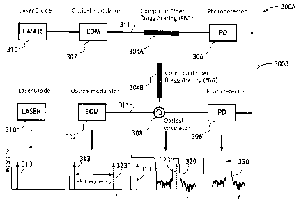
Referring now to FIG. 3, a diagrammatic view of filters 300A and 300B of the
present invention
is shown. The filters 300A and 300B are particular implementations of the
filter 200 of FIG. 2.
Similar numerals in FIGs. 2 and 3 refer to similar elements. The filter 300A
uses a fiber Bragg
grating (FBG) 304A in transmission, while the filter 300B uses an FBG 304B in
reflection. An
optical circulator 308 is incorporated into the optical path of the filter
300B having the reflection
FBG 304B. A beamsplitter, not shown, can be used instead of the optical
circulator 308.
The filters 300A and 300B of FIG. 3 have a laser diode 310 for emitting light
at the carrier
frequencyfc, an optical modulator 302 for receiving light from the laser 310
and for modulating
light with an input electrical signal, the FBGs 304A and 304B, respectively,
coupled to the
optical modulator 302, for receiving the modulated light and for filtering
light, and a
photodetector 306 coupled to the FBGs 304A and 304B, respectively, for
detecting a signal at a
beat frequency between the frequencies of the filtered light. The signal
detected by the
photodetector 306 is the output electrical signal of the filters 300A and
300B.
8
CA 02696066 2010-03-09
Doc No: 102-47 CA Patent
The FBGs 304A and 304B have an optical response function 320. In the
transmission FBG
304A this response function 320 is the transmitted response, and in the
reflection FBG 304B this
response function 320 is the reflected response. The laser diode 310, the
optical modulator 302,
the FBGs 304A and 304B, and the photodetector 306 are optically coupled with
an optical fiber
311 as shown in FIG. 3.
In general, to characterize a spectral response of an electrical filter, a
frequency-swept electrical
signal is applied to the filter input, and an output electrical signal is
measured. The output
electrical signal plotted against the frequency of the swept signal represents
the response
function of the filter being characterized. Accordingly, to obtain a spectral
response of the filters
300A or 300B, a frequency-swept electrical signal can be applied to the
modulator 302. As a
result of modulation, a component 323' appears in the optical spectrum of the
signal at the output
of the modulator 302. The separation between the component 323' and a signal
313 at the carrier
frequencyfc corresponds to the frequency of modulation by the modulator 302.
The signal is filtered by the FBGs 304A or 304B having the spectral response
320. Both signals
313 and 323' co-propagate through the FBGs 304A or 304B. As mentioned
previously, the other
sideband 223" is suppressed. At the detector 306, the optical signals
interfere with each other to
generate an signal at a beat frequency therebetween. As the electrical signal
is swept in
frequency, the component 323' is shifted relative to the carrier frequency
component 313,
resulting in attenuation of the component 323' by the FBGs 304A or 304B when
the component
323' shifts beyond the passband of the optical attenuation spectrum 320 of the
FBGs 304A or
304B. The output electrical signal at the photodetector plotted against the
frequency of the swept
signal will form a spectral response 330 corresponding to the optical
attenuation spectrum 320 of
the FBGs 304A or 304B. Therefore, by adjusting the optical attenuation
spectrum 320, one can
adjust the electrical response function 330 of the filters 300A or 300B.
The compound FBGs 304A or 304B are tunable by tuning its temperature, or by
stress-tuning, or
by tuning any other suitable parameter thereof. The FBGs 304A and 304B may be
superstructure gratings, multi-phase shift gratings, and/or chirped gratings.
These types of
gratings are described by Raman Kashyap in a book entitled "Fiber Bragg
Gratings", Academic
Press, ISBN 0-12-400560-8, 1999, which is incorporated herein by reference. In
particular,
9
CA 02696066 2010-03-09
Doe No: 102-47 CA Patent
Figures 3.24, 6.5 and 7.1 of the above reference show the above stated
respective types of the
gratings. Other types of gratings can also be used, with or without
apodization, including
gratings in planar waveguides.
The laser diode 310 can be a distributed-feedback (DFB) laser. DFB lasers are
frequency tuned
by tuning the laser temperature using a thermoelectric cooler (TEC), not
shown. Thus, by
adjusting the temperature of the TEC, the filter 300A and 300B can be tuned in
frequency.
Alternatively, the laser diode 310 can have an external FBG serving as a
mirror of the lasing
cavity of the laser diode 310. The laser FBG, not shown, can also be
temperature tuned. The
laser diode 310 can be modulated directly, in which case no optical modulator
302 will be
required.
Furthermore, the filters 300A and 300B, or the filter 200 for that matter, can
be implemented
using a planar waveguide technology. For example, the optical modulator 202,
the optical filter
204, and the detector 206 can be implemented on a common planar substrate,
coupled by a
planar optical waveguide. Integrating the filter 200 of FIG. 2 using planar
waveguide technology
may further improve the stability and manufacturability of the filter 200.
Turning now to FIG. 4, a measured transmission spectrum 400 of the FBG 304A of
FIG. 3 is
shown. The spectrum 400 has two passbands 401 and 402. The first passband 401
is for
filtering light at the sidelobe frequency 323', and the second passband 402 is
for passing the
carrier component 313 at the carrier frequencyfc. When the transmission FBG
304A is tuned,
for example by adjusting the grating temperature, the spectrum 400 shifts
towards higher or
lower frequencies, as shown at 400' and 400". As the spectrum 400 shifts, the
first passband 401
and the second passband 402 shift together. When the first passband shifts,
the signal 323'at the
sidelobe frequency is either passed or attenuated, because the passband 401 is
narrow. However,
the second passband 402 is wide enough to always pass the carrier component
313. As a result,
mixing of the output signal 323', if any, with a signal at the carrier
frequencyfc is always
available; and tuning of the transmission FBG 304A results in tuning the
spectral response
function 330 of the filter 300A. Preferably, the passband 401 is tunable by at
least 2GHz,
allowing the filter 300A to operate in a 2GHz wide frequency band, for example
between the
frequencies of 18GHz and 20GHz.
CA 02696066 2010-03-09
Doc No: 102-47 CA Patent
Referring to FIG. 5, the compound transmission FBG 304A of FIG. 3 is shown in
FIG. 5 as
consisting of two FBGs 501 and 502 connected in series. Advantageously, having
two FBGs 501
and 502 allows both the central frequency and the bandwidth of the filter 300A
to be
independently tuned, as explained in more detail below.
Turning to FIGs. 6A to 6C, transmission bands 601 and 602 of FBGs 501 and 502
are shown,
respectively. The purpose of FIGs. 6A to 6C is to illustrate bandwidth tuning
of the filter 300A
of FIG. 3 by tuning FBGs 501 and 502 of FIG. 5. FBGs 501 and 502 of FIG. 5 may
be tuned by
tuning the grating temperature or any other suitable grating parameter.
In FIG. 6A, the transmission bands 601 and 602 do not overlap each other, so
that there is no
passband. In FIG. 6B, the transmission bands 601 and 602 are shifted towards
each other as
shown by arrows 603 and 604. The transmission bands 601 and 602 form a
passband in an
overlap region 605 therebetween. The passband is centered at the filter
frequency fF and has a
finite bandwidth dfF1. In FIG. 6C, the transmission bands 601 and 602 are
shifted towards each
other even closer than in FIG. 6B, forming a passband having a wider bandwidth
dfF2 > AIFM.
Thus, shifting the transmission bands of the FBGs 501 and 502 towards each
other or away from
each other results in tuning the bandwidth of the filter 300A.
Turning to FIGs. 7A to 7C, transmission bands 701 and 702 of FBGs 501 and 502
are shown,
respectively. The purpose of FIGs. 7A to 7C is to illustrate central frequency
tuning of the filter
300A of FIG. 3 by tuning FBGs 501 and 502 of FIG. 5.
In FIG. 7A, the transmission bands 701 and 702 form a passband in an overlap
region 705
therebetween, shifted from the carrier frequency signal 313 by dl. In FIG. 7B,
the transmission
bands 701 and 702 are shifted equally towards higher frequencies as shown by
arrows 703 and
704. The passband is shifted from the carrier frequency signal 313 by 42 > dl.
In FIG. 7C, the
passband is shifted from the carrier frequency signal 313 by 43 > d2 > dl.
Thus, shifting the
transmission bands of the FBGs 501 and 502 in the same direction results in
tuning the central
frequency of the passband of the filter 300A. It should be noted that both the
central frequency
and the bandwidth can be tuned together by tuning only one FBG, 501 or 502.
11
CA 02696066 2010-03-09
Doc No: 102-47 CA Patent
The bandwidth of the passband of the FBG 304A and the roll-off of the passband
will strongly
affect the filtering characteristics of the filter 300A. The bandwidth will
determine the largest
possible bandwidth of the filter 300A. The largest bandwidth is reached when
the central
frequencies of the two FBGs 501 and 502 coincide. Making the FBG bandwidth as
large as
possible would allow a wide range of bandwidth tuning of the filter 300A.
However, a wide
passband has the detrimental effect of reducing the filter roll-off of the
passband, thus reducing
out-of-band attenuation. Increasing the slope of the filter roll-off will
limit the narrowest
bandwidth of the filter 300A. Narrow-passband FBGs 501 and 502 will have a
steeper spectral
slope and attenuate out-of-band information more strongly. Therefore, a trade-
off exists between
the filter bandwidth and the out-of-band rejection. An optimization of the FBG
transmission
spectrum is required, depending on particular requirements of a specific radio-
frequency filter
application.
It should be noted that an FBG with a properly selected transmission spectrum
can also be used
to implement a low-pass or a high-pass microwave filter with variable centre
frequency and
bandwidth. It should also be noted that the above considerations and
principles illustrated in
FIGs. 4, 5, 6A to 6C, and 7A to 7C having regard to the transmission FBG 304A
used in the
filter 300A are also applicable to the reflection FBG 304B used in the filter
300B. In the latter
case, proper reflection spectra should be considered instead of the
transmission spectra.
Referring now to FIG. 8, an attenuation spectrum 800 of an FBG used in the
present invention,
for example the FBG 501 or 502, is shown. The transmission band is defined by
a 3dB
bandwidth parameter; a frequency offset at a 20dB attenuation point relative
to a corresponding
edge of the 3dB passband; and a frequency offset at a 35dB attenuation point
relative to a
corresponding edge of the 3dB passband; a ripple value and group delay for the
filter passband;
and a separation value between carrier and filter passbands. These parameters
can be used to
specify an FBG suitable for use in a particular radio-frequency filter. The
useful ranges of these
parameters can be obtained from target specifications of the radio-frequency
filter 300A of FIG.
3. FIG. 8 shows an example of filter passband parameters of such a filter.
Other filter passband
configurations can be easily realized using this invention.
12
CA 02696066 2010-03-09
Doc No: 102-47 CA Patent
A filter with specifications defined in FIG. 8 can be designed using
techniques described by
Raman Kashyap in the article entitled "Fiber Bragg Gratings", Academic Press,
ISBN 0-12-
400560-8, 1999, which is incorporated herein by reference. Other techniques
known to a person
skilled in the art may be used as well.
A tunable filter of the present invention is usable in space subsystems due to
wide tunability, low
mass, low volume, and low power consumption. However, it should be understood
that a
tunable filter of the present invention can also be used in other
communication systems requiring
flexible bandwidth allocation and center frequency tuning. Furthermore, wide
tunability of the
filter warrants its application as a "set-and-forget" fixed filter, which is
tuned once at the factory
and shipped to a customer based on the customer's frequency specification.
Further, a filter of the present invention is not intended to only be used for
a RF frequency range.
For example, a filter using properly selected components can, in principle, be
constructed to
operate in microwave, mm-wave, terahertz and other frequency ranges.
13