Note : Les descriptions sont présentées dans la langue officielle dans laquelle elles ont été soumises.
CA 02699680 2015-07-29
55182-6
RFID PATCH ANTENNA WITH COPLANAR REFERENCE GROUND AND
= FLOATING GROUNDS
[0001) This application claims priority to U.S. Application No.
60/978,389, entitled
"RFID PATCH ANTENNA WITH COPLANAR REFERENCE GROUND AND
FLOATING GROUNDS", filed on October 8, 2007.
FIELD OF THE INVENTION
[0002] = The present invention relates generally to a low-cost,
low thickness, compact,
wideband patch antenna with radiating element and reference ground conductor
in the same
geometric plane or closely spaced parallel planes, and optionally including
floating ground
= conductors in the same geometric plane or closely spaced parallel planes,
said patch antenna
or arrays of such patch antennas having utility in radio frequency
identification (RFID)
applications in which UHF-band signals are passed between a reader
(transceiver) and a tag
(transponder) via the patch antenna. The invention is of particular use in
RFID applications
in which it is desirable to create a space with well-controlled directional
UHF signal emission
above a surface such as a smart shelf, smart counter-top or other RFID-enabled
surface,
which space contains a collection of RFID tagged items, and such that the
items in the space
= can be dependably read using UHF signals from the RFID reader attached to
the antenna,
without the complication =of null zones or locations in the space at which the
UHF signals are
too weak to communicate with RFID tags.
BACKGROUND ART
[00031 = Radio frequency identification (RFID) systems and other
forms of electronic
article surveillance are increasingly used to track items whose locations or
dispositions are of
some economic, safety, or other interest. In these applications, typically,
transponders or tags
= are attached to or placed inside the items to be tracked, and these
transponders or tags are in
at least intermittent communication with transceivers or readers which report
the tag (and, by
inference, item) location to people or software applications via a network to
which the readers
=are directly or indirectly attached. Examples of RFID applications include
tracking of retail
CA 02699680 2010-03-15
WO 2009/048982
PCT/US2008/079247
Atty Dkt No. 043057-0375402 (VUE-058 PCT)
Filed via PCT EFS on 10/8/2008
items being offered for public sale within a store, inventory management of
those items
within the store backroom, on store shelving fixtures, displays, counters,
cases, cabinets,
closets, or other fixtures, and tracking of items to and through the point of
sale and store exits.
Item tracking applications also exist which involve warehouses, distribution
centers, trucks,
vans, shipping containers, and other points of storage or conveyance of items
as they move
through the retail supply chain. Another area of application of RFLD
technology involves
asset tracking in which valuable items (not necessarily for sale to the
public) are tracked in an
environment to prevent theft, loss, or misplacement, or to maintain the
integrity of the chain
of custody of the asset. These applications of RFLD technology are given by
way of example
only, and it should be understood that many other applications of the
technology exist.
[00041 RFED systems typically use reader antennas to emit
electromagnetic carrier
waves modulated and encoded with digital signals to REED tags. As such, the
reader antenna
is a critical component facilitating the communication between tag and reader,
and
influencing the quality of that communication. A reader antenna can be thought
of as a
transducer which converts signal-laden alternating electrical current from the
reader into
signal-laden oscillating electromagnetic fields or waves appropriate for a
second antenna
located in the tag, or alternatively, converts signal-laden oscillating
electromagnetic fields or
waves (sent from or modified by the tag) into signal-laden alternating
electric current for
demodulation by and communication with the reader. Types of antennas used in
RFLD
systems include patch antennas, slot antennas, dipole antennas, loop antennas,
and many other
types and variations of these types.
[0005) In the case of passive RFLD systems, the RFLD tag is powered by
the
electromagnetic carrier wave. Once powered, the passive tag interprets the
radio frequency
(RF) signals and provides an appropriate response, usually by creating a
timed, intermittent
disturbance in the electromagnetic carrier wave. These disturbances, which
encode the tag
response, are sensed by the reader through the reader's antenna. In the case
of active RFID
systems the tag contains its own power source, such as a battery, which it can
use to either
initiate RF communications with the reader by creating its own carrier wave
and encoded RF
signals, or else the tag power can be used to enhance the tag performance by
increasing the
tag's data processing rate or by increasing the power in the tag's response,
and hence the
maximum distance of communication between the tag and reader.
2
CA 02699680 2010-03-15
WO 2009/048982
PCT/US2008/079247
Atty Dkt No. 043057-0375402 (VUE-058 PCT)
Filed via PCT EFS on 10/8/2008
[00061 Especially for passive RFID systems, it is often convenient to
distinguish the
behavior of RFID systems and their antennas in terms of near-field versus far-
field behavior.
"Near-field" and "far-field" are relative terms, and it is with respect to the
wavelength of the
carrier wave that the terms "near" and "far" have meaning. When the distances
involved in an
application are much greater than the wavelength, the application is a far-
field application,
and often the antenna can be viewed as a point-source (as in most
telecommunications
applications). On the other hand, when the distances involved in an
application are much
shorter than the wavelength, the relevant electromagnetic interactions between
antennas (e.g.,
reader antenna and tag antenna) are near-field interactions. In such a
situation the reactive
electric or magnetic component dominates the EM field, and the interaction
between the two
coupled antennas occurs via disturbances in the field. When the application of
interest
involves distances on the order of the wavelength of the carrier wave, the
situation is more
complex and cannot be thought of as simply near-field or simply far-field.
Below this
situation will be termed "mid-field".
[0007] Two common frequency bands used by commercial RFID systems are
13.56MHz and UHF (approximately 850 to 960MHz, with the specific band
depending on the
country in question). Since a tag on an RFID-tagged consumer item is generally
used for
many applications throughout the supply chain, from manufacturing and
distribution to the
final retail store location, the functional requirements of retail shelves are
only one of the sets
of factors influencing the choice of tag frequency. There are many factors and
requirements
of interest to various trading partners in the supply chain, and in this
complex situation both
13.56MHz and UHF are used extensively for tracking tagged items on and in
smart shelving,
racks, cabinets, and other retail, warehouse, and other business fixtures.
U.S. Patents
7,268,742, 6,989,796, 6,943,688, 6,861,993, 6,696,954, 6,600,420, and
6,335,686 all deal
with RFID antenna applications to smart shelves, cabinets, and related
fixtures. 13.56MHz
waves have a wavelength ofjust over 22 meters (72 feet), while the wavelength
of UHF
radiation used in RFID applications is approximately a third of a meter, or
just one foot.
Since the distances characteristic of item-level RFID applications involving
the tracking and
surveillance of tagged items on or in shelves, cabinets, racks, counters, and
other such
fixtures are on the order of feet (e.g., 0.5 ft to several feet), it is clear
that, when UHF
technology is used, the antenna interactions are neither near-field nor far-
field, but rather are
mid-field. In this case, a poor choice of reader antenna type, or the poor
design of a proper
3
CA 02699680 2010-03-15
WO 2009/048982
PCT/US2008/079247
Atty Dkt No. 043057-0375402 (VUE-058 PCT)
Filed via PCT EFS on 10/8/2008
type, can result in poor performance of the overall RFID system and
application failure. One
of the reasons for this is that in a mid-field situation the electric and
magnetic fields emitting
from the reader antenna vary significantly over the relevant surface (e.g.,
the surface of a
retail shelf holding tagged items). The field may be strong in one place and
much weaker in
another place a few inches away (because the wavelength of UHF radiation is
only a few
inches), and the general behavior of the UHF system is much more complex than
is observed
in 13.56MHz applications. Thus, in situations where UHF tags are used in RFID
item
tracking on shelves and other storage fixtures, the design of the reader
antenna becomes
critical. The current invention describes an approach to UHF antenna design
which results in
a uniform UHF emission zone immediately above the surface of the antenna
(e.g., shelf
surface) without large null (no-read) areas, and without requirement of a
large antenna
thickness which would limit the usefulness of the antenna design in practical
retail and other
business applications.
[0008] The detection range of passive RFID systems is typically limited
by signal
strength over short ranges, for example, frequently less than a few feet for
passive UHF RFID
systems. Due to this read range limitation in passive UHF RFID systems, many
applications
make use of portable reader units which may be manually moved around a group
of tagged
items in order to detect all the tags, particularly where the tagged items are
stored in a space
significantly larger than the detection range of a stationary or fixed reader
equipped with one
fixed antenna. However, portable UHF reader units suffer from several
disadvantages. The
first involves the cost of human labor associated with the scanning activity.
Fixed
infrastructure, once paid for, is much cheaper to operate than are manual
systems which have
ongoing labor costs associated with them. In addition, portable units often
lead to ambiguity
regarding the precise location of the tags read. For instance, the reader
location may be noted
by the user, but the location of the tag during a read event may not be known
sufficiently well
for a given application. That is, the use of portable RFID readers often leads
to a spatial
resolution certainty of only a few feet, and many applications require
knowledge of the
location of the tagged items within a spatial resolution of a few inches.
Portable RFID
readers can also be more easily lost or stolen than is the case for fixed
reader and antenna
systems.
[0009] As an alternative to portable UHF RFID readers, a large fixed
reader antenna
driven with sufficient power to detect a larger number of tagged items may be
used.
4
CA 02699680 2010-03-15
WO 2009/048982 PCT/US2008/079247
Atty Dkt No. 043057-0375402 (VUE-058 PCT)
Filed via PCT EFS on 10/8/2008
However, such an antenna may be unwieldy, aesthetically displeasing, and the
radiated power
may surpass allowable legal or regulatory limits. Furthermore, these reader
antennas are
often located in stores or other locations were space is at a premium and it
is expensive and
inconvenient to use such large reader antennas. In addition, it should be
noted that when a
single large antenna is used to survey a large area (e.g., a set of retail
shelves, or an entire
cabinet, or entire counter, or the like), it is not possible to resolve the
location of a tagged
item to a particular spot on or small sub-section of the shelf fixture. In
some applications it
may be desirable to know the location of the tagged item with a spatial
resolution of a few
inches (e.g., if there are many small items on the shelf and it is desired to
minimize manual
searching and sorting time). In this situation the use of a single large
reader antenna is not
desirable because it is not generally possible to locate the item with the
desired spatial
resolution.
[0010] Alternatively, a fully automated mobile antenna system can be
used. U.S.
Patent 7,132,945 describes a shelf system which employs a mobile or scanning
antenna. This
approach makes it possible to survey a relatively large area and also
eliminates the need for
human labor. However, the introduction of moving parts into a commercial shelf
system may
prove impractical because of higher system cost, greater installation
complexity, and higher
maintenance costs, and inconvenience of system downtime, as is often observed
with
machines which incorporate moving parts. Beam-forming smart antennas can scan
the space
with a narrow beam and without moving parts. However, as active devices they
are usually
big and expensive if compared with passive antennas.
[0011] To overcome the disadvantages of the approaches described above,
fixed
arrays of small antennas are utilized in some UHF RFID applications. In this
approach
numerous reader antennas spanning over a large area are connected to a single
reader or group =
of readers via some sort of switching network, as described for example in
U.S. Patent
7,084,769. Smart shelving and other similar applications involving the
tracking or inventory
auditing of small tagged items in or on RFID-enabled shelves, cabinets, cases,
racks, or other
fixtures can make use of fixed arrays of small antennas. In tracking tagged
stationary items in
smart shelving and similar applications, fixed arrays of small antennas offer
several
advantages over portable readers, systems with a single large fixed antenna,
and moving-
antenna systems. First, the antennas themselves are small, and thus require
relatively little
power to survey the space surrounding each antenna. Thus, in systems which
query these
CA 02699680 2010-03-15
WO 2009/048982
PCT/US2008/079247
Atty Dkt No. 043057-0375402 (VUE-058 PCT)
Filed via PCT EFS on 10/8/2008
antennas one at a time, the system itself requires relatively little power
(usually much less
than 1 watt). By querying each of the small antennas in a large array, the
system can thus
survey a large area with relatively little power. Also, because the UHF
antennas used in the
antenna array are generally small and (due to their limited power and range of
less than 1-12
inches) survey a small space with a specific known spatial location, it must
also be true that
the tagged items read by a specified antenna in the array are also located to
the same spatial
resolution of 1-12 inches. Thus systems using fixed arrays of small antennas
can determine
the location of tagged items with more precision than portable RFID readers
and systems
using a small number of relatively large antennas. Also, because each antenna
in the array
is relatively small, it is much easier to hide the antennas inside of the
shelving or other
storage fixture, thus improving aesthetics and minimizing damage from external
disruptive
events (e.g., children's curiosity-driven handling, or malicious activity by
people in general).
Also, an array of fixed antennas involves no moving parts and thus suffers
from none of the
disadvantages associated with moving parts, as described above. Also, small
antennas like
those used in such antenna arrays may be cheaper to replace when a single
antenna element
fails (relative to the cost of replacing a single large antenna). Also, fixed
arrays of antennas
do not require special manual labor to execute the scanning of tagged items
and, therefore, do
not have associated with them the high cost of manual labor associated with
portable reader
and antenna systems, or with mobile cart approaches.
[0012] In smart shelving and similar applications it is often important
for economic
and aesthetic reasons that the antennas used in the antenna array be simple,
low cost, easy to
retrofit into existing infrastructure, easy to hide from the view of people in
the vicinity of the
antennas, and that the antennas can be installed and connected quickly. These
application
requirements are more easily met with an antenna configuration which minimizes
the number
of layers used in the antenna fabrication, and which also minimizes the
overall antenna
thickness. That is, thin or low profile antennas are easier to hide, and
easier to fit into
existing infrastructure without requiring special modification to that
existing infrastructure.
Also, reducing layers in the antenna tends to reduce antenna cost. For reasons
of cost and
installation convenience it is also desirable to have the simplest possible
approach to the
attachment of the RF feed cables or wires to the antennas. Preferably, the
attachment should
be made in one location, on one surface, without requiring a hole or special
channel, wire, or
conductive via through the antenna substrate. This last requirement is
especially important in
6
CA 02699680 2010-03-15
WO 2009/048982
PCT/US2008/079247
Atty Dkt No. 043057-0375402 (VUE-058 PCT)
Filed via PCT EFS on 10/8/2008
large-volume manufacture of the antenna systems since, in that case, the final
assembly will
usually involve a few hand assembly steps carried out by an electronics
technician on an
assembly line, and elimination of one or several steps will significantly
reduce the total
production cost. It is also important that the design of the UHF antennas
allows for reading
of RFID tags in the space near the antennas without "dead zones" or small
areas between and
around antennas in which the emitted fields are too weak to facilitate
communication between
the tag and reader. Another requirement for the antennas used in smart shelf
and similar
applications is that they have the ability to read items with a diversity of
tag antenna
orientations (i.e., tag orientation independence, or behavior at least
approaching that ideal).
[0013] Traditional patch antennas, slot antennas, dipole antennas, and
other common
UHF antenna types which might be used in antenna systems such as those
described above
generally involve multiple layers. U.S. Patent 6,639,556 shows a patch antenna
design with
this layered structure and a central hole for the RF feed. U.S. Patent
6,480,170 also shows a
patch antenna with reference ground and radiating element on opposing sides of
an
intervening dielectric. A multi-layer antenna design can lead to excessive
fabrication cost and
excessive antenna thickness (complicating the retrofitting of existing
infrastructure during
antenna installation, and making it more difficult to hide the antennas from
view). Multi-
layer antenna designs also tend to complicate the form of the attachment of
the connecting
wires (for example, co-axial cable between the antenna and reader) since the
connections of
the signal carrier and reference ground occur on different layers, and this
increases the cost of
the antenna for the reasons described above.
[0014] For UHF smart shelving applications the patch antenna is a good
choice of
antenna type because the fields emitted from the patch antenna are
predominantly in the
direction orthogonal to the plane of the antenna, so the antenna can be placed
on or inside the
shelf surface and create an RFID-active space in the region immediately above
the shelf, and
read the tagged items sitting on the surface of the shelf with relative ease.
Of course, this
presupposes that the particular patch antenna design yields sufficient
bandwidth and radiation
efficiency to create, for a given convenient and practical power input, a
sufficiently large
space around the antenna wherein tagged items can be dependably and
consistently read. The
traditional patch antenna described in the prior art has a main radiative
element of conductive
material fabricated on top of a dielectric material. Beneath (i.e., on the
reverse side of) the
dielectric material is typically located a reference ground element, which is
a planar layer of
7
CA 02699680 2010-03-15
WO 2009/048982
PCT/US2008/079247
Atty Dkt No. 043057-0375402 (VUE-058 PCT)
Filed via PCT EFS on 10/8/2008
conductive material electrically grounded with respect to the signals being
transmitted or
received by the antenna. In the typical patch antenna design well known in the
prior art, the
antenna main radiative element and the reference ground element are in
parallel planes
separated by the dielectric material (which, in some cases, is simply an air
spacer). Also, in
the usual case, the main radiative element and the reference ground element
are fabricated
with one directly above the other, or with one substantially overlapping with
the other in their
respective parallel planes. A disadvantage of this traditional multi-layer
patch antenna
design is that the connection of the shielded cable or twisted pair wire
carrying signals
between the antenna and the RFID reader must be attached to the antenna on two
separate
levels separated by the dielectric material, thus requiring a connecting hole
or via in the
dielectric layer.
[0015] The size of the gap between the radiating element and the
reference ground
conductor (i.e., the dielectric layer thickness) is a critical design
parameter in the traditional
patch antenna since, for a given dielectric material, the thickness of this
gap largely
determines the bandwidth of the antenna. As the gap is reduced, the bandwidth
is narrowed.
If the bandwidth of the antenna is too narrow, the tuning of the antenna in a
given application
becomes very difficult, and uncontrollable changes in the environment during
normal
operation (such as the unanticipated and random introduction of metal objects,
human hands,
or other materials into the area being monitored by the antenna) can cause a
shift in resonance
frequency which, combined with the overly narrow bandwidth, causes failure in
RFID tag
detection and reading. Thus, for a given application there is for practical
reasons a lower
limit on the distance between the ground plane and the radiating element in a
traditional patch
antenna design, and this constrains the overall thickness of the antenna.
[0016] Another constraint on the thickness of a traditional patch antenna
stems from
radiation efficiency (fraction of total electrical energy put into the antenna
which is emitted as
electromagnetic radiation). If the dielectric thickness or gap between the
reference ground
and radiating element is too small, the radiating efficiency will be too low,
and too much of
the power to the antenna is wasted as heat flowing into the dielectric and
surroundings.
[0017] The discussion above makes it clear that (1) a patch antenna
design can be
used effectively in UHF smart shelf and similar applications, and (2) use of
the patch type of
antenna would be even more advantageous, and satisfy the previously discussed
practical
requirements of smart shelving more completely if there were some way of
overcoming the
8
CA 02699680 2010-03-15
WO 2009/048982
PCT/US2008/079247
Atty Dkt No. 043057-0375402 (VUE-058 PCT)
Filed via PCT EFS on 10/8/2008
constraints on the thickness of the antenna imposed by the requirements of
high bandwidth
and radiation efficiency. Also, it would be advantageous to find a new design
for the patch
antenna which simplifies the attachment of the feed cable or wire. In
addition, it would be
advantageous to find a new antenna design which spread the UHF radiation more
evenly and
over a greater area of the surface of the shelf containing the antenna (i.e.,
in the region above
the radiating element plane) than is possible for the traditional patch
antenna design. As
noted above, the relatively short wavelength (approximately 12 inches) of UHF
emissions can
present challenges to the designers of UHF smart shelving who want to be able
to effectively
and consistently read tags at any location on the shelf. A better UHF antenna
design would
minimize this problem, and allow better "field spreading" or "field shaping"
in the regions
immediately above and around the edges of the antenna.
[0018] The current invention overcomes the above-mentioned limitations
of the
traditional patch antenna design, and results in a new patch antenna which is
much thinner
without sacrificing bandwidth and radiation efficiency. Also, the current
invention allows for
a much more simple antenna feed cable attachment than is possible with the
traditional patch
antenna approach. Also, the current invention allows for a more evenly
distributed UHF field
around the antenna which makes it easier to avoid dead zones, and allows the
smart shelf
designer to spread or shape the field evenly around the antenna. In contrast
to this prior art,
the current invention describes an antenna in which the main radiative element
is placed in a
common geometric plane, or substantially the same plane, with the reference
ground element,
or in which the main radiative element and reference ground element are placed
in two
parallel, closely spaced planes separated by a dielectric laminate, with
little or no overlap
between the main radiative element and the reference ground element. That is,
a key
invention described in this specification is a patch antenna in which the main
radiative
element and the reference ground element are in the same plane, or in two
closely-spaced
parallel planes, with the two elements substantially side-by-side rather than
one directly over
the other, or rather than one substantially overlapping with the other. This
cost-efficient
antenna configuration, particularly when implemented with a floating ground
plane or planes
in addition to the reference ground element, and with the floating ground
plane or planes
located beneath the plane holding the main radiative element and reference
ground, results in
superior antenna gain, bandwidth, and tuning robustness in RFID smart shelf
applications, as
well as similar applications in which it is desired to interrogate a number of
RFID tags
9
CA 02699680 2015-07-29
55182-6
= located in close proximity, with low-power RFID signals localized in a
small physical space
which would normally result in tuning difficulties for traditional patch
antennas. A further
advantage of the current invention is that the newly invented patch antenna is
thinner than a
typical patch antenna described in the prior art. That is, by locating the
main radiative
element and the reference ground element in the same plane, or substantially
the same plane =
with little or no overlap, a thinner patch antenna can be designed for a given
high bandwidth,
radiative efficiency, and robust frequency response requirement.
SUMMARY OF THE INVENTION
[0019) In accordance with the preferred embodiment of the
invention, reader antennas
are provided within storage fixtures (for example, shelves, cabinets, drawers,
or racks) for
= transmitting and receiving RF signals between, for example, an RFID
reader and an RFlD tag
or transponder. The reader antennas may be placed in a variety of
configurations which
include but are not limited to configurations in which, for each antenna, the
main radiative
antenna element and the reference ground element for the antenna are located
within the same
= physical or geometric plane, or in two parallel closely spaced planes
separated by a dielectric
laminate, with little or no overlap between the radiative antenna element and
the reference
ground element.
[00201 Also, as an option, one or more floating ground plane(s)
may be included in
the same plane as or in a plane parallel to the radiative antenna element's
geometric plane to
improve, control, or optimize the electric or magnetic field strength or shape
around the
antenna.
= [0021] In the preferred embodiment, the RFID-enabled
storage fixtures are equipped
with multiple patch antennas, each patch antenna having its own reference
ground element
coplanar with or substantially coplanar with the respective patch antenna's
main radiative
element.
[0022] Furthermore, in the preferred embodiment, these RFID-
enabled fixtures are
implemented using an intelligent network in which the antennas are selected,
activated, and
otherwise managed by a supervisory control system consisting of one or more
controllers and
= a host computer or host network.
CA 02699680 2015-07-29
55182-6
10022a1 According to one aspect of the invention, there is provided an
antenna
assembly, comprising: a planar laminate; a planar electrically conductive area
of
predetermined shape and dimension forming a radiative antenna element on the
planar
laminate, and another planar electrically conductive area of predetermined
shape and
dimension forming a reference ground element on the planar laminate, such that
the radiative
antenna element and the reference ground element are coplanar, and wherein
there is no
substantial overlap between the radiative antenna element and the reference
ground element; a
first planar electrically conductive floating ground element that is oriented
parallel to the
radiative antenna element and the reference ground element, and that is
separated from the
planar laminate by an air-filled space, and that is electrically connected
directly to the
radiative antenna element; and a second planar electrically conductive
floating ground
element on the planar laminate and coplanar with the radiative antenna element
and the
reference ground element; wherein the radiative antenna element is
substantially larger than
the reference ground element and the second floating ground element.
[0022b1 According to another aspect of the invention, there is provided a
method of
making an antenna assembly comprising the steps of: providing a planar
laminate; forming a
planar electrically conductive area of predetermined shape and dimension into
a radiative
antenna element on the planar laminate, and forming another planar
electrically conductive
area of predetermined shape and dimension into a reference ground element on
the planar
laminate, such that the radiative antenna element and the reference ground
element are planar
with each other, and wherein there is no substantial overlap between the
radiative antenna
element and the reference ground element; providing a first planar
electrically conductive
floating ground element that is oriented parallel to the radiative antenna
element and the
reference ground element, that is separated from the planar laminate by an air-
filled space,
and that is electrically connected directly to the radiative antenna element;
providing a second
planar electrically conductive floating ground element on the planar laminate,
wherein the
second floating ground element is substantially smaller than the radiative
antenna element and
is coplanar with the radiative antenna element and the reference ground
element; and
10a
CA 02699680 2015-07-29
55182-6
attaching a connection element that electrically connects each of the
radiative antenna element
and the reference ground element.
[00231 These and other aspects and advantages of the various embodiments
will be
described herein below.
10b
CA 02699680 2010-03-15
WO 2009/048982
PCT/US2008/079247
Atty Dkt No. 043057-0375402 (VUE-058 PCT)
Filed via PCT EFS on 10/8/2008
BRIEF DESCRIPTION OF THE DRAWINGS
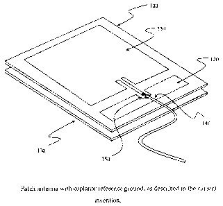
[0024] FIG. I shows a patch antenna design typical of the prior art.
[0025] FIG. 2 shows a patch antenna with coplanar reference ground, as
described in
the current invention.
[0026] FIG. 3 shows a detail drawing of the coaxial cable connection to
the antenna
patch and reference ground planes, as described in the current invention.
[0027] FIG. 4 shows examples of alternative patch antenna shapes.
[0028] FIG. 5 shows an example of a patch antenna in which an additional
floating
ground element has been placed in the same plane as that containing the
radiative antenna
element and reference ground element.
[0029] FIG. 6 shows an array of patch antennas of varying orientation.
[0030] FIG. 7 shows a prior art patch antenna corresponding to the
computer
simulation results provided in the detailed description of the current
invention.
[0031] FIG. 8 shows the return loss (band width) plot for the prior art
patch antenna,
of design shown in FIG. 7.
[0032] FIG. 9 shows a coplanar reference ground patch antenna without
floating
ground element, corresponding to computer simulation results provided in the
detailed
description of the current invention.
[0033] FIG. 10 shows the return loss (band width) plot for the coplanar
reference
ground patch antenna without floating ground element, of design shown in FIG.
9.
[0034] FIG. 11 shows the return loss (band width) plot for a coplanar
reference
ground patch antenna with floating ground element.
DETAILED DESCRIPTION OF THE INVENTION
[0035] Preferred embodiments and applications of the current invention
will now be
described. Other embodiments may be realized and changes may be made to the
disclosed
embodiments without departing from the spirit or scope of the invention.
Although the
preferred embodiments disclosed herein have been particularly described as
applied to the
field of RFID systems, it should be readily apparent that the invention may be
embodied in
any technology having the same or similar problems.
[0036] In the following description, a reference is made to the
accompanying
drawings which form a part hereof and which illustrate several embodiments. It
is understood
11
CA 02699680 2010-03-15
WO 2009/048982
PCT/US2008/079247
Atty Dkt No. 043057-0375402 (VUE-058 PCT)
Filed via PCT EFS on 10/8/2008
that other embodiments may be utilized and structural and operational changes
may be made
without departing from the scope of the descriptions provided.
[0037] FIG. 1 is a drawing showing a patch antenna from the prior art.
In this design
the supporting dielectric material 100 separates the radiative antenna element
110 (top side of
the dielectric) and the reference ground element 120 (bottom side of the
dielectric). Feed
point 135 requires a hole in the dielectric so that the ground element of the
feed cable (not
shown) can be attached to the reference ground 120.
[0038] FIG. 2 is a drawing illustrating an exemplary patch antenna
assembly in
accordance with the preferred embodiment of the current invention. In the
preferred
embodiment a first supporting dielectric material 100 like that commonly used
in printed
circuit boards is used to support the radiative antenna element 110 and
reference ground
element 120. Floating ground 130 is a solid metal sheet or is printed on the
circuit board,
and is separated from the first printed circuit board by an air-filled space.
The size of the air
space or gap is maintained in the preferred embodiment by a non-conductive
support which
holds the edges of the two printed circuit boards at a fixed distance of
separation. The
antenna patch 110, reference ground 120 and floating ground 130 are typically
comprised of
solid copper metal plating, but it should be immediately clear to those
skilled in the art that
other types of electrically conductive materials may be used for these
elements of the antenna
assembly. Signals are fed to the antenna at point 150 where, in the preferred
embodiment, a
coaxial cable has been attached with the cable's core conductor soldered to
the radiative
antenna element and the cable shielding mesh soldered to the reference ground
element, as
shown. In the preferred embodiment the total separation between the antenna
patch 110 and
the floating ground 130 is between 0.125 inches and 0.5 inches, but larger or
smaller
separations can also be used. The rigid dielectric laminates supporting the
antenna patch 110,
reference ground 120, and floating ground 130 are typically between 0.025
inches and 0.060
inches, while thickness of other flexible materials, such as Mylar or FR4 or
other similar
material, can be as low as a few mils. Easy feeding is an obvious advantage of
this
configuration since the radiative antenna element 110 and the reference ground
element 120
are in the same plane and situated close to each other.
[0039] In one embodiment of making the Figure 2 embodiment patch
antenna, the
radiative antenna element, also referred to as patch 110, and the reference
ground element
120 can be fabricated by copper or other metal patterns etched or patterned or
deposited onto
12
CA 02699680 2010-03-15
WO 2009/048982
PCT/US2008/079247
Atty Dkt No. 043057-0375402 (VUE-058 PCT)
Filed via PCT EFS on 10/8/2008
the surface of the dielectric material 100, which can be a polyester or other
plastic or polymer
sheet, such as Mylar or FR4.
[0040] The antenna assembly shown in FIG. 2 provides wide bandwidth with
three
resonant frequencies, which is realized by placing the reference ground
element in the same
plane with the radiative antenna element. Because the reference ground is a
metalized
rectangular patch, it generates the third resonant frequency when it is
coupled to the main
(radiative) patch. This third resonant frequency can be tuned by adjusting the
dimensions of
the reference ground. The sizes of the reference ground element and radiative
antenna
element, the distance between the reference ground element and the radiative
antenna
element, and the feeding location are determined by the resonance frequency
band, the
bandwidth, and polarization requirements. By carefully selecting the values
for the variables
mentioned above, one can produce an antenna with three resonance peaks
spreading over the
desired band. The high antenna bandwidth of the current invention is one of
the most
important advantages over the prior art antenna designs.
[0041] In the preferred embodiment of the current invention a physical
connection
(via an electrical conductor not shown in FIG. 2) is often made between the
radiative antenna
element 110 and the floating ground 130. Because of this electric DC short
between the
radiative element and the floating ground, there is no DC voltage difference
between them,
and this connection greatly reduces the tendency for the electronic system to
experience
failure due to ESD (electrostatic discharge).
[0042] FIG. 3 shows in more detail the connection of a coaxial cable 140
to the
antenna patch 110 and reference ground 120. In the preferred embodiment of the
invention
the coaxial cable is a shielded cable commonly used in RFID and other radio
frequency
applications. Typically the RF signal is carried by voltage variations in the
cable's copper
core 144, relative to or referenced to the voltage in the cable's metal mesh
shielding wrap
142. The core 144 and shielding wrap 142 are separated by a dielectric
insulation material
143. In the preferred embodiment the cable core 144 is soldered to the antenna
patch 110
with solder 148, and the shielding wrap 142 is soldered to the reference
ground 120 with
solder 146. Alternatively, different types of connectors, such as SMA, can
also be used to
connect the antenna and the system.
100431 The antenna, in its various embodiments as described in the
current invention
(and in other embodiments which after consideration of the structures and
approaches taught
13
CA 02699680 2015-07-29
=
55182-6
in the current invention may be easily conceived by one skilled in the art)
may be fed by an
RF signal from external circuitry (not shown) through a means such as a
coaxial cable, as
shown in FIG. 2. The external circuitry may be, for example, a switch device,
an RFID
reader, an intelligent network (as described in U.S. Patent Application Number
11/366,496,
which claims priority to US Provisional Application No. 60/673,757), or any
known
component or system for transporting RF signals to and from an antenna
structure. It should
be recognized that the antenna feed point or point of attachment shown in FIG.
2 and FIG. 3
is only one example, and it is also possible to attach the core 144 to other
points on the
antenna patch 110. Also, it is possible to choose various points of attachment
for the
= shielding wrap 142 on the reference ground 120. The particular choice of
these points of
attachment depend upon the antenna bandwidth and gain required in the
particular antenna
application, and upon the application-specific requirements for the shape and
symmetries of
the electric and magnetic fields to be established by the antenna. The
attachment alternatives
are too numerous to be enumerated here, but should be clear to one skilled in
the art, after
consideration of the structures and approaches taught, by way of example, in
the current
invention.
[00441 It should be clear to one skilled in the art that the
coaxial cable 140 shown in
the figures of the current invention may be replaced by any other appropriate
cable, cord, or
wire set capable of carrying the signal and reference voltages needed in the
application
addressed by the current invention, and this replacement may be made without
departing from
the scope of the current invention.
[00451 The radiative antenna element 110 may be implemented in any
pattern or
geometrical shape (e.g., square, rectangular, circle, free flow, etc.).
Several of these shape
alternatives are shown in FIG. 4, including a rectangular shape 310,
rectangular shape with=
trimmed corners along one diagonal 320, rectangular shape with a slot 330,
rectangular shape
with two orthogonal slots 340, circular shape 350, circular shape with a slot
360, and circular
shape with two orthogonal slots 370. These alternatives are shown by way of
example only
and are not intended to limit the scope and application of the current
invention.
[00461 The radiative antenna element 110 may be made up of a metal
plate, metal
foil, printed or sprayed electrically conductive ink or paint, metal wire
mesh, or other
functionally equivalent material (e.g., film, plate, metal flake, etc.). The
material of antenna
substrate 100 is a dielectric material (e.g., the material typically used for
printed circuit
14
=
CA 02699680 2010-03-15
WO 2009/048982
PCT/US2008/079247
Atty Dkt No. 043057-0375402 (VUE-058 PCT)
Filed via PCT EFS on 10/8/2008
boards) or any other material having negligible electrical conductivity
(including a
combination of two or more different types of such negligibly conductive
material, as may be
used in a laminated or layered structure).
[0047] The cable 140 may have at either end, or located along its
length, tuning
components (not shown) such as capacitors and inductors. The sizes (e.g.,
capacitance or
inductance) of these tuning components are chosen based on the desired
matching and
bandwidth characteristics of the antenna, according to practices well known to
those skilled in
the art.
[0048] The feed points for the radiative antenna element 110 and
reference ground
element 120, the separation distance between the radiative antenna element 110
and reference
ground element 120, the shapes of the radiative antenna element 110 and
reference ground
element 120, the size and placement of slots or other voids in the radiative
antenna element
110 and/or reference ground element 120, as well as the presence or absence of
the floating
ground 130, its size and shape, the separation distance between the radiative
antenna element
110 and the floating ground 130, and the location of or presence of an
electrical connection or
"short" between the radiative antenna element 110 and floating ground 130, may
each
individually or together be adjusted to optimize the antenna gain, the shapes
of the electric
and magnetic fields set up by the antenna when driven by a particular signal,
and the power
consumed by the antenna when driven by that signal. Also, the above
characteristics of the
antenna and its various components, particularly the characteristics of
antenna element slots,
slits, and cut corners, can be adjusted to reach the desired antenna size and
cause the antenna
to be polarized in a direction favorable for reading RFID tags placed on
objects to be detected
by the antenna. For example, the antenna may be given a linear polarization in
a direction
favorable for reading tags placed upon objects in a particular orientation.
The tag location or
position may cooperate with the antenna polarization, if any, for favorably
reading the tag.
The details of the slits or slots, and nature of the cut comers, also have a
significant effect on
the frequency response of the antenna, and can be used to increase the
bandwidth of the
antenna. The third resonant frequency introduced by the use of one or more
floating ground
elements extends the bandwidth, while a traditional patch antenna only has one
or two
resonant frequencies.
[0049] For antenna designs typical of the prior art, the placement of
metal objects
below the antenna changes the resonance frequency of the antenna and can cause
serious
CA 02699680 2010-03-15
WO 2009/048982
PCT/US2008/079247
Atty Dkt No. 043057-0375402 (VUE-058 PCT)
Filed via PCT EFS on 10/8/2008
detuning. This problem has been greatly relieved by the current invention. The
antenna
structure of the preferred embodiment of the current invention performs well
even when a
metal plate or other conductive object is placed closely below the antenna
structure (such as a
metal retail or storage shelf) due to the constrained EM field. Because the
floating ground
introduced for the metal shelf works as a reflector, the radiation can only
happen in one
direction. Therefore, the antenna has higher gain, but usually reduced
bandwidth.
[0050J FIG. 5 shows an example of a patch antenna in which the radiative
antenna
element 110, reference ground element 120, and one floating ground element 160
have been
placed in a common plane. In this example, another floating ground plane 130
is also present
in a second plane. Placing a floating ground element in the same plane as the
reference
ground and radiative element gives greater bandwidth. FIG. 5 shows only one
additional
(coplanar) floating ground, but more than one can be employed to shape the
fields around the
antenna and optimize the radiation pattern for the application at hand.
[00511 Detailed computer simulations were undertaken to demonstrate some
of the
advantages of the current invention relative to the prior art. FIG. 7 shows a
particular
embodiment of the prior art patch antenna having a square radiative antenna
element with cut
corners (for production of circularly polarized fields), and a square
reference ground element
in a plane below the plane of the radiative antenna element. The distance A in
FIG. 7 is 4.65
inches, and distance B is 1.3 inches. Note that the corner cuts were made at a
45 degree
angle. The distance C (edge length of the reference ground element) is 8
inches. The
distance D between the two planes in FIG. 7 is 0.5 inches. The feed point for
the antenna in
FIG. 7 is located 2.975 inches from the side of the radiative element
(distance E) and 0.415
inches from the front edge of the radiative element (distance F). In the
simulation, air was
used as the dielectric between the two planes. Copper properties were used for
the radiative
element and the reference ground. The substrate supporting the radiative
element and the
reference ground was assumed to be FR402 (62 mils thick), a common substrate
material
used in the printed circuit board industry. The material surrounding the
antenna was
assumed to be air. FIG. 8 shows the return loss in dB, as a function of
frequency, for the
antenna described by FIG. 7. At -8dB, the bandwidth exhibited is approximately
13%. At -
10dB the bandwidth is about 10%.
[00521 FIG. 9 shows a particular embodiment of the current invention
having a square
radiative antenna element with 45-degree cut corners and a coplanar
rectangular reference
16
CA 02699680 2010-03-15
WO 2009/048982
PCT/US2008/079247
Atty Dkt No. 043057-0375402 (VUE-058 PCT)
Filed via PCT EFS on 10/8/2008
ground element. The distance A in FIG. 9 is 3.94 inches, and the distance B is
1.34 inches.
The length C of the reference ground element 120 is 5.28 inches, and its width
G is 0.63
inches. The gap H between the radiative antenna element 110 and the reference
ground
element 120 is 0.28 inches. As in the simulation corresponding to the antenna
in FIGS. 7
and 8, that of FIG. 9 assumed copper properties for the radiative element and
the reference
ground. The substrate supporting the radiative element and the reference
ground was
assumed to be FR402, with a thickness of 62 mils. The material surrounding the
antenna
was assumed to be air. FIG. 10 shows the return loss in dB, as a function of
frequency, for
the antenna described by FIG. 9. At -8dB, the bandwidth exhibited is
approximately 30%.
At -10dB the bandwidth is about 20%. Thus, the bandwidth of the antenna of the
current
invention is significantly greater than that of the prior art, as demonstrated
in these simulation
results.
[0053] Additional simulations were carried out in which a floating
ground element
was placed 0.5 inches below the antenna of FIG. 9. The resulting return loss
plot is shown in
FIG. 12. Note the introduction of additional resonance peaks by the presence
of the floating
ground element. The bandwidth of this antenna design is less than that of the
antenna shown
in FIG. 9 (without a floating ground), but greater than the bandwidth of the
prior art patch
antenna shown in FIG. 7.
[0054] In another embodiment of the current invention, the patch antenna
assembly of
FIG. 2 can be used in the form of an array of antenna assemblies, as shown in
FIG. 6. Similar
to the antenna assembly of FIG. 2, each antenna assembly in the array of FIG.
6 may have its
own radiative antenna element 110, reference ground element 120, and feed
cable 140. In
one embodiment of the current invention, all of the antennas in the array can
be mounted on a
single (common) printed circuit board and make use of a single (common)
floating ground
element. Alternatively, a separate substrate and floating ground element can
be used for each
antenna assembly in the array.
[0055] In an array such as that shown in FIG. 6, the orientation of each
antenna
assembly (with respect to orientation around an imaginary axis perpendicular
to the radiative
antenna element and running through its center) can be varied, or else each
antenna assembly
in the array may have the same rotational orientation.
[0056] By arranging antenna assemblies into an array such as that shown
in FIG. 6, it
is possible to cover a larger physical area on a retail store shelf,
storehouse or distribution
17
CA 02699680 2015-07-29
55182-6
center rack, counter top, or other physical space of relevance in an RFID tag
reading
application, or other RF communications application. In such an approach, a
relatively large
number of relatively small antennas can be used, with each antenna in the
array being queried,
as required, by the antenna network control system, host RFID reader, or other
host system.
Examples of such networks and control systems can be found in U.S. Patent
Application
Number 11/366,496, which claims priority to US Provisional Application No.
60/673,757.
[0057] In an additional embodiment of the current invention, the
array of antenna
assemblies, such as but not limited to the example shown in FIG. 6, may be
enclosed in a
housing, fixture, or shell, such as a retail store shelf, cabinet, warehouse
shelf or rack, retail
store countertop, or some other commercial or home storage or work fixture.
The material
used in the housing, fixture, or shell may be selected from a wide variety of
materials,
including wood, plastic, paper, laminates made from combinations and
permutations of wood,
plastic, and paper, or metal, or combinations of metal and other dielectric
materials. In such
housings, fixtures, or shells enclosing the array of antenna assemblies, the
placement of any
and all metal components may be made according to the demands of structure
strength,
integrity, and aesthetics, in such a way as to allow electromagnetic fields
from the antennas in
= the array to be projected out into the space above, below, or around the
housing, fixture, or
shell, such as the application may demand.
[0058] One embodiment of the current invention, described by way
of example, is a
solid metal retail shelf upon which an antenna assembly array, such as that
shown in FIG. 6,
is placed with the antenna patch and reference ground side of the antenna
assemblies facing
up and away from the metal shelf, and fixed in place with adhesive or metal
screws, and
covered with a plastic shell for protection of the antenna components and
improvement of the
= aesthetics as required in the application. For such an embodiment, and in
the case of other
embodiments which might be imagined which have solid and relatively extensive
pieces of
metal on the floating ground side of the antenna assemblies, the highly
directional gain of the
antenna created by the configuration of the radiative antenna element 110,
reference ground
element 120, and floating ground 130 create a desirable situation in which the
behavior of the
antennas, including their tuning and gain, are insensitive to variations in
the size, shape,
conductivity, and other characteristics of the metal shelf upon which the
array of antenna
= assemblies has been placed. This is because the floating ground creates
uniformity of electric
CA 02699680 2010-03-15
WO 2009/048982
PCT/US2008/079247
Atty Dkt No. 043057-0375402 (VUE-058 PCT)
Filed via PCT EFS on 10/8/2008
potential in its plane and shields everything beyond it (on the side opposite
the patch) from
the electric and magnetic fields which would otherwise be emitted on that side
of the antenna.
In other words, the use of the floating ground in between the radiative
antenna element /
reference ground plane and the metal of the shelf makes the antenna assembly
"one-sided" in
its behavior, and keeps the oscillating fields on the upper side of the
antenna assembly (on the
side of the antenna assembly opposite the metal of the shelf). This
insensitivity to the
particulars of the design of the metal shelf offers greater flexibility in the
application of a
single antenna assembly array design to multiple and varied shelf fixtures,
and eliminates the
need for extensive re-design or customization of the patch antenna when moving
from one
application to another.
[0059] In another embodiment of the current invention, the metal of the
retail shelf
may itself be used as a floating ground or, alternatively, the shelf may be
constructed such
that a common sheet of metal is used as both a floating ground plane and also
a physical
support for the antenna assembly or antenna assembly array, as well as objects
which may be
placed upon the fixture, such as retail items holding RFID tags.
[0060] The current invention explicitly includes and encompasses all
embodiments
which may be imagined by variation of one or more features of the embodiments
described in
this specification, including radiative antenna element size, shape,
thickness, void or slot
shape, reference ground element size, shape, placement within the two
dimensions of the
plane occupied by the radiative antenna element, distance separating the
radiative antenna
element and reference ground element, position and manner of attachment of the
signal feed
line or cable to the radiative antenna element and reference ground element,
presence or
absence of one or more floating ground elements, size, shape, or thickness of
the floating
ground plane, separation distance between the floating ground and the
radiative antenna
element, the dielectric material or materials used to separate the radiative
antenna element
from the reference ground and floating ground, the conductive material or
materials used to
fabricate the radiative antenna element, reference ground, and floating
ground, the number of
antenna assemblies used in the array, or materials and structures used to
house and protect the
antenna assembly or antenna assembly array.
[0061] The current invention also encompasses all embodiments in which
the antenna
assembly array is replaced by a single antenna assembly (i.e., with a single
patch antenna).
19
CA 02699680 2010-03-15
WO 2009/048982
PCT/US2008/079247
Atty Dkt No. 043057-0375402 (VUE-058 PCT)
Filed via PCT EFS on 10/8/2008
[0062] It should also be noted that various arrays of antenna assemblies
may be
constructed in which the antenna assemblies occupy two different planes. For
example, one
may build an array of antenna assemblies in which some of the assemblies are
located inside a
first geometric plane, and the remainder of the assemblies are located inside
a second
geometric plane orthogonal to the first geometric plane. This embodiment is
given by way of
example only, and it should be noted that the two planes need not necessarily
be orthogonal.
Also, it is conceivable that more than two geometric planes may be used in the
placement of
the antenna assemblies. Such a multi-planar array of antenna assemblies may
improve the
robustness of the array in some applications in which, for instance, the
orientation of the
RFID tags to be interrogated by the antennas is not known, or is known to be
random or
varying. In addition, the application may demand specific electrical or
magnetic field
polarization which may be produced by placement of the antenna assemblies in
several
planes. All of the embodiments which may be imagined for the placement of
multiple
antenna assemblies in multiple planes are explicitly included in the current
invention.
[0063] Other embodiments of the current invention may be imagined in
which the
radiative antenna element 110 of the antenna assembly shown in FIG. 2 is
replaced with a slot
antenna, antenna loop or planar coil, or some other type of antenna radiator
element. Such a
replacement can be imagined in any of the invention embodiments described in
this
specification, and all of the additional embodiments which can be imagined by
such as
replacement are explicitly included in the current invention.
[0064] While embodiments have been described in connection with the use
of a
particular exemplary shelf structure, it should be readily apparent any shelf
structure, rack,
etc. (or any structure, such as antenna board, shelf back, divider or other
supporting structure)
may be used in implementing the invention, preferably, for use in selling,
marketing,
promoting, displaying, presenting, providing, retaining, securing, storing, or
otherwise
supporting an item or product.
[0065] Although specific circuitry, components, modules, or dimensions
of the same
may be disclosed herein in connection with exemplary embodiments of the
invention, it
should be readily apparent that any other structural or functionally
equivalent circuit(s),
component(s), module(s), or dimension(s) may be utilized in implementing the
various
embodiments of the invention. It is to be understood therefore that the
invention is not
CA 02699680 2010-03-15
WO 2009/048982
PCT/US2008/079247
Atty Dkt No. 043057-0375402 (VUE-058 PCT)
Filed via PCT EFS on 10/8/2008
limited to the particular embodiments disclosed (or apparent from the
disclosure) herein, but
only limited by the claims appended hereto.
21