Note : Les descriptions sont présentées dans la langue officielle dans laquelle elles ont été soumises.
CA 02704099 2015-01-30
RESTART CIRCUIT FOR MULTIPLE LAMP ELECTRONIC BALLAST
[0001]
FIELD OF THE INVENTION
[0002] The present invention generally relates to
electronic ballasts for providing power to a pair of lamps.
More particularly, the invention is concerned with causing
the ballast to restart in response to replacing either of
the lamps.
BACKGROUND OF THE INVENTION
[0003] Ballasts for powering two fluorescent lamps
simultaneously start the lamps when power is received from a
power supply such as a household power switch (i.e., 120V
AC). Starting the ballast includes checking for fault
conditions and, upon finding no faults, driving a switching
operation of an inverter of the ballast to provide power to
the lamps via a resonant circuit of the ballast. When a lamp
is disconnected from the ballast or a fault occurs with one
of the lamps (e.g., a filament breaks or becomes
nonconductive), the ballast prevents the inverter from
performing the switching operation. That is, the inverter is
shut down. The inverter remains shut down until the power to
the ballast from the power supply is disconnected and
subsequently reconnected, or until a monitored
1
CA 02704099 2010-05-13
filament of the two lamps is disconnected from the ballast and
subsequently reconnected, causing a restart (i.e., relamping) of
the ballast. For example, if a user removes and replaces the
lamp having the monitored filament, the ballast automatically
restarts when the lamp is reconnected to the ballast (e.g.,
reinserted into a fixture containing the ballast). If the user
instead removes and replaces the other lamp, not having the
monitored filament, the ballast shuts off when the lamp is
removed, and remains off even after the lamp is reconnected to
the ballast. The user must remove and replace the lamp having
the monitored filament, or cycle the power to the ballast (i.e.,
turn the power to the ballast off and back on) in order to
restart the ballast.
SUMMARY OF THE INVENTION
[0004] Aspects of the invention include an electronic
ballast and method for causing a restart (i.e., relamping) of
the ballast in response to a user replacing either of a first
lamp or a second lamp powered by the ballast. The ballast
includes a controller, an inverter, a resonant circuit, a
filament health check circuit, and a dv/dt (voltage rate of
change or voltage slope) circuit. The controller compares a
first current, representative of a current through a second
filament of the second lamp, to a second current, wherein the
second current is a reference current. If a determined ratio of
the first current to the second current is less than or equal to
a predetermined ratio, then the controller prevents a switching
operation of the inverter. If the determined ratio is greater
than the predetermined ratio, then the controller drives the
switching operation of the inverter. The controller restarts
the ballast in response to the determined ratio transitioning
from below the predetermined ratio to equal to or above the
2
CA 02704099 2015-01-30
predetermined ratio. The dv/dt circuit reduces the first
-current for a transient time period in response to a
disturbance of a direct current (DC) component of a
current through a second filament of the first lamp,
causing the ballast to relamp or restart when either of
the first lamp or the second lamp is reconnected to the
ballast. The determined ratio may be the ratio of the
second current to the first current. Additionally, or
alternatively, the controller may prevent the switching
operation of the inverter if the determined ratio is
greater than a predetermined ratio, and drive the
switching operation of the inverter if the determined
ratio is less than the predetermined ratio, without
deviating from the scope of the invention.
[0004a] According to an aspect, there is provided a
ballast to power a first lamp and a second lamp, the first
lamp having a first filament and a second filament, and the
second lamp having a first filament and a second filament,
the ballast comprising: a rectifier configured to receive
alternating current power from a power supply and to provide
a direct current (DC) voltage to a DC voltage bus; an
inverter configured to receive power from the DC voltage bus
and to provide AC power during execution of a switching
operation; a resonant circuit configured to receive the AC
power provided by the inverter, the resonant circuit
comprising: a first output pair for connecting across the
first filament of the first lamp, a second output pair for
connecting across the second filament of the first lamp and
the first filament of the second lamp, wherein the second
filament of the first lamp is in series with the first
3
CA 02704099 2015-01-30
,
filament of the second lamp, and a third output pair for
,
- connecting across the second filament of the second lamp; a
controller configured to monitor a first current and a
second current, wherein the first current is a DC current
through at least one of the filaments of the lamps and the
second current is a reference current, the controller
further configured to determine a ratio of the first current
to the second current, and to control the switching
operation of the inverter as a function of the determined
ratio, wherein: the controller inhibits the switching
operation of the inverter when the determined ratio of the
first current to the second current is less than or equal to
a predetermined ratio, the controller drives the switching
operation of the inverter when the determined ratio is more
than the predetermined ratio, and the controller restarts
the ballast in response to the ratio transitioning from
below the predetermined ratio to above the predetermined
ratio; and a dv/dt circuit configured to reduce the first
current for a transient time period in response to a rapid
voltage change at the second output pair; wherein the
connection of at least one lamp filament to the resonant
circuit causes the dv/dt circuit to reduce the first current
for the transient time period, resulting in the determined
ratio falling below the predetermined ratio for the
transient time period.
[0004b] According to another aspect, there is
provided a method of restarting a ballast that is powering a
first lamp and a second lamp, in response to replacement of
either lamp, each of the lamps having a first filament and a
second filament, the method comprising: monitoring a first
current and a second current, wherein the first current is a
3a
CA 02704099 2015-01-30
direct current (DC) current through at least one of the
- filaments of the lamps and the second current is a reference
current; determining a ratio of the first current to the
second current; controlling a switching operation of an
inverter of the ballast via a controller of the ballast as a
function of the determined current ratio, the controlling
comprising: inhibiting the switching operation of the
inverter when the determined ratio is less than or equal to
a predetermined ratio; and driving the switching operation
of the inverter when the determined ratio is higher than the
predetermined ratio; reducing the first current for a
transient time period in response to a rapid voltage change
at the second filament of the first lamp, wherein the
determined ratio falls below the predetermined ratio for the
transient time period due to the reduction of the first
current; and restarting the ballast in response to the
determined ratio falling below the predetermined ratio and
subsequently increasing to at least the predetermined ratio.
[0005] Other objects and features will be in part
apparent and in part pointed out hereinafter.
BRIEF DESCRIPTION OF THE DRAWINGS
[0006] FIG. 1 is a schematic diagram, partially in
block form, of an electronic ballast to power a lamp
according to one embodiment of the invention.
[0007] FIG. 2 is a partial schematic diagram of a
controller of the electronic ballast of FIG. 1 according
to one embodiment of the invention.
[0008] FIG. 3 is a schematic diagram of the ballast
of FIG. 1 according to one embodiment of the invention.
3b
CA 02704099 2015-01-30
[0009] Corresponding reference characters indicate
' corresponding parts throughout the drawings.
DETAILED DESCRIPTION
[0010] Referring to FIG. 1, an electronic ballast 100
receives AC power from an alternating current (AC) power
supply 102 (e.g., standard 120V AC household power). The
ballast 100
3c
CA 02704099 2010-05-13
comprises a rectifier 104, an inverter 110, a resonant circuit
112, a controller 114, a dv/dt (voltage rate of change or
voltage slope) circuit 116, a filament health check circuit 160,
and miscellaneous resistors, capacitors, and terminals. The
rectifier 104 converts the AC power, received from the AC power
supply 102, to direct current (DC) power. Various optional
components may be connected to or internal to the rectifier 104
for conditioning and/or altering the DC voltage output of the
rectifier 104. These include, but are not limited to, a bus
capacitor (shown as element C1 in FIG. 1), a voltage regulator
(not shown), a voltage limiter (not shown), a power factor
correction circuit (not shown), and a DC-to-DC converter (not
shown). The rectifier 104 outputs a DC voltage on a DC voltage
bus 106 and a ground 108 for the ballast 100. The optional
capacitor C1, connected between the DC voltage bus 106 and the
ground 108, conditions the DC voltage transmitted via the DC
voltage bus 106. The inverter 110 is connected to the DC
voltage bus 106 and the ground 108. When driven by the
controller 114, the inverter 110 provides an AC output to the
resonant circuit 112. In some embodiments, the inverter may be
a half bridge inverter.
[0011] During steady state operation, the controller 114
drives a switching operation of the inverter 110 by using a
pulse width modulation unit 214, which is part of the controller
114. The controller 114 driving the switching operation of the
inverter 110 results in the inverter 110 providing power to the
resonant circuit 112. The resonant circuit 112, in turn, uses
the provided power to power a first lamp L1 and a second lamp
L2. Each of the lamps L1, L2 includes a first filament and a
second filament, and each of the filaments includes a first
terminal and a second terminal. The resonant circuit includes a
first output pair 121, a second output pair 122, and a third
4
CA 02704099 2010-05-13
output pair 123. In some embodiments, the resonant circuit may
include a resonant inductor (e.g., inductor L4-A shown in FIG.
3) and a resonant capacitor (e.g., capacitor C16 shown in FIG.
3).
[0012] The output pairs of the resonant circuit 114 are
connected to the lamps L1, L2 as follows. The first output pair
121 is connected across a first filament 130 of the first lamp
L1. That is, the first output pair 121 is connected to the
first terminal 144 and the second terminal 146 of the first
filament 130 of the first lamp L1. The second output pair 122
is connected to the second terminal 142 of the second filament
132 of the first lamp L1 and to the first terminal 150 of the
first filament 134 of the second lamp L2. The ballast 100 also
connects the first terminal 148 of the second filament 132 of
the first lamp L1 to the second terminal 152 of the first
filament 134 of the second lamp L2. The third output pair 123
is connected across the second filament 136 of the second lamp
L2. That is, the third output pair 123 is connected to the
first terminal 156 of the second filament 136 of the second
lamp, and to the second terminal 154 of the second filament of
the second lamp. Each of the first output pair 121, second
output pair 122, and third output pair 123 has a first terminal
and a second terminal for connecting to the corresponding first
or second terminals of the lamps L1, L2, such that the terminals
144, 146, 142, 148, 150, 152, 154, and 156 can be referred to as
the terminals of the output pairs or of the filaments.
[0013] The controller 114 prevents the switching operation
of the inverter 110 if the controller determines that the second
filament 136 of the second lamp L2 is not electrically
conductive. For example, the second lamp L2 may be broken, not
intact, or may otherwise be disconnected from the third output
pair 123. A filament health check circuit 160 is for detecting
CA 02704099 2010-05-13
a fault in the second filament 136 of the second lamp L2. The
filament health check circuit 160 includes a resistance R25.
The filament health check circuit 160 provides the first current
to the controller 114 when the second filament 136 of the second
lamp L2 is connected to the third output pair 123 regardless of
whether the other filaments are connected to the other output
pairs. In the electronic ballast 100 shown in FIG. 1, the
filament health check circuit also includes resistors R31, R21,
and R23. The resistance R25 is connected between the DC voltage
bus 106 and the first terminal 156 of the third output pair 123.
The second terminal 154 of the third output pair 123 is
connected to the first current input 160 of the controller 114
via resistors R31, R21, and R23. Thus, the first current is at
least in part representative of a DC current from the DC bus to
the controller through the second filament 136 of the second
lamp L2. A resistive network comprising resistors R29, R33, and
R22 provides a reference current to a second current input 162
of the controller 114. Thus, the reference current may herein
be referred to interchangeably as the second current. The
controller 114 compares the first current to the second current
and determines a ratio of the first current to the second
current. If the determined ratio is less than or equal to a
predetermined ratio, the controller 114 prevents the switching
operation of the inverter 110. That is, the controller 114
prevents the inverter 110 from powering the resonant circuit 112
and the lamps L1 and L2. If the determined ratio is more than
the predetermined ratio, the controller 114 drives the switching
operation of the inverter 110 to provide power to the resonant
circuit 112 and the lamps L1 and L2. In some embodiments, the
predetermined ratio may be 3/4. When the determined ratio, as
determined by the controller 114, transitions from below the
predetermined ratio to the predetermined ratio, the controller
6
CA 02704099 2010-05-13
114 checks the electronic ballast 100 and the lamps L1 and L2
for faults. Faults may include, but not limited to, end of lamp
life, filaments not intact, and rectifier effect. The
controller 114 restarts the electronic ballast 100 if the
controller 114 finds no faults.
[0014] Referring to FIG. 2, the controller 114 of FIGS. 1,
2, and 3B receives the first current at the first current input
160. The anode of a first controller diode 206 is connected to
the first current input 160, and the cathode of the first
controller diode 206 is connected to a first side a first
controller resistor 208. A second side of the first controller
resistor 208 is connected to an operating voltage node 216 of
the controller 114. The anode of a second controller diode 202
is connected to the second current input 162, and the cathode of
the second controller diode 202 is connected to a first side a
second controller resistor 204. A second side of the second
controller resistor 204 is connected to the operating voltage
node 216 of the controller 114. In some embodiments, a
capacitor (not shown in FIG. 2) may be connected between the
operating voltage node 216 and the ground 108. The controller
also includes a comparator 210 having a negative input connected
to the cathode of the second controller diode 202 and a positive
input connected to the cathode of the first controller diode
206. An output of the comparator 210 is connected to a logic
circuit 212 of the controller 114. The logic circuit 212
determines whether to prevent or drive the switching operation
of the inverter 110. The logic circuit 212 loads parameters
into a pulse width modulation (PWM) unit 214 of the controller
114 for driving or preventing the switching operation of the
inverter 110. The PWM unit 214 drives the inverter as a
function of the loaded parameters. When the first and second
currents are supplied to the controller 114, the operating
7
CA 02704099 2010-05-13
voltage node 216 develops an operating voltage for the
controller 114, and the controller draws an operating current
from the node, enabling start up of the electronic ballast 100.
In some embodiments, the controller may be an 0S2331418 or
ICB2FLOSRAM available from Infineon Technologies, AG of
Neubiberg, Germany. The controller 114 also analyzes the first
current and the second current to determine other lamp problems,
such as but not limited to end of lamp life and rectifier
effect.
[0015] Referring again to FIG. 1, the dv/dt circuit 116
reduces the first current for a transient time period in
response to replacement of the first lamp Ll or the second lamp
L2. The dv/dt circuit 116 comprises a first resistor R44, a
second resistor R46, a first capacitor C28, a third resistor
R45, a second capacitor C27, and a switch Q5. The first
resistor R44 is connected between the first terminal 156 of the
third output pair 123 and the first terminal 152 of the second
output pair 122. The second resistor R46 has a high side
connected to the second terminal 142 of the second output pair
122 and a low side connected to the ground 108. The first
capacitor C28 has an input side connected to the high side of
the second resistor R46. The output side of the first capacitor
C28 is connected to a high side of third resistor R45, and a low
side of the third resistor R45 is connected to the ground 108.
The second capacitor C27 is connected in parallel with the third
resistor R45. The switch Q5 has an input connected to the
output side of the first capacitor C28, a low side connected to
the ground 108, and a high side connected to the first current
input 160 of the controller 114. In the electronic ballast 100
shown in FIG. 1, the dv/dt circuit 116 also includes, and in
some embodiments may optionally include, a second capacitor C27
connected in parallel with the third resistor R45, a first diode
8
CA 02704099 2010-05-13
D12 connected in parallel with the third resistor R45 with its
anode connected to the ground 108, a second diode D13 connected
in parallel with the second resistor R46 with its anode
connected to the ground 108, and a third capacitor C33 connected
in parallel with the second resistor R46. Also in the
electronic ballast 100 shown in FIG. 1, the input side of the
first capacitor C28 is connected to the first terminal 142 of
the second output pair 122 via a fourth resistor R47, and the
high side of the switch Q5 is connected to the first current
input 160 via a fifth resistor R34.
[0016] In operation, the dv/dt circuit 116 monitors a
voltage of the second output pair 122 connected to the second
terminal 142 of the first lamp L1 for a rapid voltage change.
Such a rapid voltage change activates a switch Q5 when a voltage
change with respect to time exceeds a threshold. The time that
the switch remains activated (i.e., the transient time period)
is a function of the values of the resistors and capacitors that
form the dv/dt circuit 116 and the time rate of change of the
monitored voltage. In the electronic ballast 100 shown in FIG.
1, the dv/dt circuit activates the switch Q5 when the second
filament 132 of the first lamp L1 or the first filament 134 of
the second lamp L2 is reconnected to the electronic ballast 100
after a period of being disconnected. The activation of the
switch Q5 causes the first current to dip, and the determined
ratio of the first current to the second current, as determined
by the controller 114, falls below the predetermined ratio.
When the transient time period passes, the first current returns
to approximately the same level as before activation of the
switch Q5, and the determined ratio of the first current to the
second current, as determined by the controller 114, now meets
or exceeds the predetermined ratio. The controller 114, in
9
CA 02704099 2010-0.5-13
response, restarts the electronic ballast 100 by driving the
switching operation of the inverter 110.
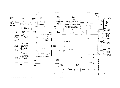
[0017] FIGS. 3A, 3B and 3C illustrate in detail an
embodiment of a light source that includes the electronic
ballast 100 shown in detail in FIG. 1, lamps Ll and L2, and the
power supply 102. The light source illustrated by FIGS. 3A, 3B
and 3C includes the inverter 110, the rectifier 104, the
resonant circuit 112, and various other components of the
electronic ballast 100 according to one embodiment of the
invention.
[0018] In FIG. 3A, transformer T1 steps up the AC line
voltage provided by power supply 102 and provides the stepped up
voltage to the rectifier 104. The rectifier 104 including
diodes D1-D4 provides the rectified voltage to a power factor
correction circuit 310, including transformers T2 and T3 and
switches Ql, Q2, and Q2A (see FIG. 3B).
[0019] In FIG. 33, the inverter 110 includes switches Q3
and Q4 controlled by the controller 114 to generate the
rectified, inverted voltage provided to the resonant circuit
112.
[0020] In FIG. 3C, the resonant circuit 112 is illustrated
and includes inductor L4-A and C16 which cooperate with
miscellaneous other inductors and capacitors illustrated in FIG.
3C to determine the resonant frequency of the resonant circuit
112. The dv/dt circuit 116 includes resistors R45, R46, and
R47, capacitors C27, C28, and C35, diodes D12 and D13, and
switch Q5.
[0021] When introducing elements of the present invention
or the preferred embodiments(s) thereof, the articles "a", "an",
"the" and "said" are intended to mean that there are one or more
of the elements. The terms "comprising", "including" and
CA 02704099 2010-05-13
"having" are intended to be inclusive and mean that there may be
additional elements other than the listed elements.
[0022] In view of the above, it will be seen that the
several objects of the invention are achieved and other
advantageous results attained.
[0023] Having described aspects of the invention in detail,
it will be apparent that modifications and variations are
possible without departing from the scope of aspects of the
invention as defined in the appended claims. As various changes
could be made in the above constructions, products, and methods
without departing from the scope of the invention, it is
intended that all matter contained in the above description and
shown in the accompanying drawings shall be interpreted as
illustrative and not in a limiting sense.
11