Note : Les descriptions sont présentées dans la langue officielle dans laquelle elles ont été soumises.
CA 02707889 2010-06-29
Multiple-input comparator and power converter
BACKGROUND OF THE INVENTION
1. Field of the Invention
[0001] The present invention relates to a field of circuit design, more
particularly
to multiple-input comparator and power converter circuits.
2. Description of Related Art
[0002] In the prior art, a pulse width modulation system usually employs a
pulse
width modulation (PWM) comparator. FIG. I is a schematic diagram showing a
comparison principle of the PWM comparator. EAO is an error amplifying
(output)
signal outputted from an error amplifier. Ramp is a saw-tooth or triangular
wave signal.
The PWM comparator is provided for comparing an error amplifying signal EAO
with
the triangular wave signal Ramp to produce a pulse width modulation (output)
signal
PWMO. When the error amplifying signal EAO is larger than the triangular wave
signal
Ramp, the PWM signal PWMO is set at high level. When the error amplifying
signal
EAO is smaller than the triangular wave signal Ramp, the PWM signal PWMO is
set at
low level. In other words, the signal level of the PWM comparator turns over
when the
error amplifying signal EAO is equal to the triangular wave signal Ramp.
[0003] The principle of pulse width modulation is that the PWM system produces
the PWM signal PWMO with different duty cycles along with the error amplifying
signal
EAO. It can be seen from FIG.1 that the duty cycle of the PWM signal PWMO
increases when the error amplifying signal EAO increases, and the duty cycle
of the
PWM signal PWMO decreases when the error amplifying signal EAO decreases. For
various types of power converters, such as DC-DC converters, DC-AC converters
or
1
CA 02707889 2010-06-29
AC-AC converters, a feedback loop circuit is usually employed for adjusting
the duty
cycle of a power switch. If the triangular wave signal Ramp has a fixed
frequency, the
modulation of pulse width is equivalent to the modulation of the duty cycle.
[0004] The triangular wave signal Ramp usually is generated by an oscillator.
A
conventional oscillator outputs a saw-tooth wave signal as shown in FIG. 1. A
valley
voltage of the saw-tooth wave signal is 0 volt. Using a buck DC-DC converter
as an
example, a duty cycle is required to equal to VONIN when a loop circuit is
stable,
where VO is the output voltage and VIN is the input voltage of the DC-DC
converter.
When the input voltage VIN is much larger than the output voltage VO , the
required
duty cycle for stable loop circuit is very small. If the valley voltage of the
saw-tooth
wave signal Ramp is equal to 0 volt, the error amplifying signal EAO needs to
be near
0 volt when the required duty cycle is very small. Thereby, an output element
of the
error amplifier may be in the saturation region and the gain of the error
amplifier
decreased significantly. As a result, the error amplifier does not function
normally.
Hence, the saw-tooth wave signal Ramp is required to be enhanced by a certain
voltage AV. FIG. 2 shows two saw-tooth wave signals before and after voltage
enhancement. Ramp1 is the saw-tooth wave signal before voltage enhancement,
Ramp2 is the saw-tooth wave signal after voltage enhancement, and AV is an
enhancement voltage.
[0005] FIG. 3 is a circuit diagram showing a conventional circuit for
enhancing a
saw-tooth wave signal Ramp. Referring to FIG. 3, the circuit comprises an
operational
amplifier OPI, an oscillator, resistors RI and R2, PMOS transistors MP1, MP2
and
MP3, and NMOS transistors MN1, MN2 and MN3. The oscillator produces the
unenhanced saw-tooth wave signal Ramp1. An intermediate node 310 between the
resistor R2 and the PMOS transistor MP3 is provided as an output terminal for
the
voltage-enhanced saw-tooth wave signal Ramp2. The saw-tooth wave signal Ramp2
2
CA 02707889 2010-06-29
is enhanced by a voltage of V1-(R2/R1) relative to the saw-tooth wave signal
Rampl.
However, the circuit is very complicated and is restricted by the responsive
speed of
the operational amplifier OP1.
[0006] For a conventional current mode power converter, the PWM signal is
generated either by adding a sampled inductance current to the saw-tooth wave
signal
Ramp, and comparing the sum with the error amplifying signal EAO from an error
amplifier, or by converting the error amplifying signal into a corresponding
current
signal, and subtracting the sampled inductance current from the corresponding
current
signal, then converting the difference back into a voltage signal, and
comparing the
saw-tooth wave signal after voltage enhancement Ramp with the voltage signal.
[0007] FIG. 4 is a schematic circuit diagram showing a conventional circuit
for
generating the PWM signal by subtracting a sampled inductance current ISEN
from an
EAO of an error amplifier and comparing the difference with the voltage-
enhanced
saw-tooth wave signal Ramp.. Referring to FIG. 4, the circuit comprises an
operational
amplifier OP2, an oscillator, an enhancement circuit, resistors R3 and R4,
PMOS
transistors MP11 and MP12, NMOS transistor MN11, a current sampling current
source, and a PWM comparator. The resistance of resistors R3 and R4 may be
equal.
- In the circuit shown in FIG. 4, RampSH is the enhanced saw-tooth wave signal
Ramp.
EAO ISEN is an output voltage showing the difference between the current
sampling
signal ISEN and the error amplifying signal EAO. The PWM comparator is
provided for
comparing the output voltage EAO_ISEN with the enhanced saw-tooth wave signal
RampSH to produce the PWM signal PWMO. The circuit is very complicated and is
restricted by the responsive speed of the operational amplifier OP2.
[0008] Thus, improved techniques for a PWM comparator are desired to
overcome the above disadvantages.
3
CA 02707889 2010-06-29
SUMMARY OF THE INVENTION
[0009] This section is for the purpose of summarizing some aspects of the
present invention and to briefly introduce some preferred embodiments.
Simplifications or omissions in this section as well as in the abstract or the
title of this
description may be made to avoid obscuring the purpose of this section, the
abstract
and the title. Such simplifications or omissions are not intended to limit the
scope of
the present invention.
[00010] According to one aspect, the present invention is a multiple-input
comparator comprising a pair of differential transistors connected by a
resister. The
gate terminals of the transistor pair serve as the input terminals of the
comparator for
receiving external voltage for comparison. The terminal of the resistor serves
as the
current input terminal and is either connected to a current source or a
current sink. .
[00011] According to another aspect, the present invention is a power
converter
utilizing the multiple-input comparator. The power inverter comprises a power
switch
driven by a PMW signal, a voltage sampling circuit, an error amplifier and a
multiple-input PWM comparator.
[00012] The present invention may be implemented in many forms. According to
one embodiment, the present invention is a multiple-input comparator
comprising: a
first differential transistor having a gate used as a first voltage input
terminal of the
multiple-input comparator to receive a first voltage; a second differential
transistor,
forming a differential transistor pair with the first differential transistor,
having a gate
used as a second voltage input terminal of the multiple-input comparator to
receive a
second voltage; and a resistor having a first terminal connected to a source
terminal of
the first differential transistor and a second terminal connected to a source
terminal of
4
CA 02707889 2010-06-29
the second differential transistor; wherein a node between the first terminal
of the
resistor and the source terminal of the first differential transistor is used
as a current
input terminal to connect to a current source, or a node between a second
terminal of
the resistor and the source terminal of the second differential transistor is
used as the
current input terminal to connect to a current sink
[00013] According to another embodiment, the present invention is a
multiple-input comparator, comprising: a first differential transistor having
a gate used
as a first voltage input terminal to receive a first voltage; a second
differential transistor,
forming a differential transistor pair with the first differential transistor,
having a gate
used as a second voltage input terminal to receive a second voltage; a first
resistor
having a first terminal connected to a source terminal of the first
differential transistor;
and a second resistor having a first terminal connected to a source terminal
of the
second differential transistor and a second terminal connected to a second
terminal
of the first resistor; wherein a node between the first terminal of the first
resistor and
the source terminal of the first differential transistor is used as a current
input terminal
to connect to a current source; or a node between the first terminal of the
second
resistor and the source terminal of the second differential transistor is used
as a
current input terminal to connect to a current sink. .
100014] According to yet another embodiment, the present invention is a power
converter, comprising: a power conversion stage comprising a power switch
driven by
a PMW signal to convert an input voltage to an output; a voltage sampling
circuit
configured for sampling the output voltage to produce a feedback voltage; an
error
amplifier configured for amplifying an error between the feedback voltage and
a
reference voltage to produce an error amplifying signal; a multiple-input PWM
comparator having a current input terminal connected to a current source or a
current
sink, a first voltage input terminal coupled with the error amplifying signal
and
CA 02707889 2010-06-29
connected to a second voltage input terminal coupled with a saw-tooth wave
signal,
for comparing the error amplifying signal with the saw-tooth wave signal to
produce a
PWM signal.
[00015] Comparing to the prior arts, with the implementation of a current
input the
present invention not only is capable of performing complicated comparison
functions,
but also has much simpler circuit structure. Other objects, features, and
advantages of
the present invention will become apparent upon examining the following
detailed
description of an embodiment thereof, taken in conjunction with the attached
drawings.
BRIEF DESCRIPTION OF THE DRAWINGS
[00016] These and other features, aspects, and advantages of the present
invention will become better understood with regard to the following
description,
appended claims and accompanying drawings, wherein:
[00017] FIG. 1 is a schematic diagram showing a comparison principle of a PWM
comparator;
[00018] FIG. 2 shows two-tooth wave signals before and after voltage
enhancement;
[00019] FIG. 3 is a circuit diagram showing a conventional circuit for
enhancing a
saw-tooth wave signal Ramp;
[00020] FIG. 4 is a schematic circuit diagram showing a conventional circuit
to
generate a PWM signal by subtracting a sampled inductance current ISEN from an
output signal EAO of an error amplifier and comparing the difference with a
voltage-enhanced saw-tooth wave signal Ramp;
6
CA 02707889 2010-06-29
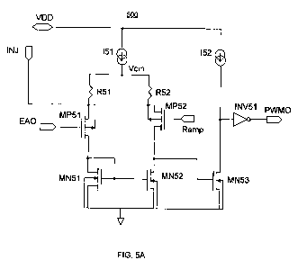
[00021] FIG. 5A is a schematic circuit diagram showing a first exemplary
configuration of a multiple-input comparator according to a first embodiment
of the
present invention;
[00022] FIG. 5B is a schematic circuit diagram showing a second exemplary
configuration of the multiple-input comparator according to the first
embodiment of the
present invention;
[00023] FIG. 5C is a schematic circuit diagram showing a third exemplary
configuration of the multiple-input comparator according to the first
embodiment of the
present invention;
[00024] FIG. 5D is a schematic circuit schematic diagram showing a fourth
exemplary configuration of the multiple-input comparator according to the
first
embodiment of the present invention;
[00025] FIG. 5E is a schematic circuit diagram showing a fifth exemplary
configuration of the multiple-input comparator according to the first
embodiment of the
present invention;
[00026] FIG. 5F is a schematic circuit diagram showing a sixth exemplary
configuration of the multiple-input comparator according to the first
embodiment of the
present invention;
[00027] FIG. 6A is a schematic circuit diagram showing a first exemplary
configuration of the multiple-input comparator according to a second
embodiment of
the present invention;
[00028] FIG. 6B is a schematic circuit diagram showing a second exemplary
configuration of the multiple-input comparator according to the second
embodiment of
the present invention;
7
CA 02707889 2010-06-29
[00029] FIG. 7 is a schematic circuit diagram showing an exemplary
configuration
of the multiple-input comparator according to a third embodiment of the
present
invention;
[00030] FIG. 8A is a schematic circuit diagram showing a first exemplary
configuration of a power converter according to one embodiment of the present
invention;
[00031] FIG. 8B is a schematic circuit diagram showing a second exemplary
configuration of the power converter according to one embodiment of the
present
invention;
[00032] FIG. 8C is a schematic circuit diagram showing a third exemplary
configuration of the power converter according to one embodiment of the
present
invention; and
[00033] FIG. 8D is a schematic circuit diagram showing a fourth exemplary
configuration of the power converter according to one embodiment of the
present
invention.
DETAILED DESCRIPTION OF THE INVENTION
[00034] The detailed description of the present invention is presented largely
in
terms of procedures, steps, logic blocks, processing, or other symbolic
representations that directly or indirectly resemble the operations of devices
or
systems contemplated in the present invention. These descriptions and
representations are typically used by those skilled in the art to most
effectively convey
the substance of their work to others skilled in the art.
[00035] Reference herein to "one embodiment" or "an embodiment" means that a
particular feature, structure, or characteristic described in connection with
the
8
CA 02707889 2010-06-29
embodiment can be included in at least one embodiment of the invention. The
appearances of the phrase "in one embodiment" in various places in the
specification
are not necessarily all referring to the same embodiment, nor are separate or
alternative embodiments mutually exclusive of other embodiments. Further, the
order
of blocks in process flowcharts or diagrams or the use of sequence numbers
representing one or more embodiments of the invention do not inherently
indicate any
particular order nor imply any limitations in the invention.
[00036] FIG. 5A is a schematic circuit diagram showing a first exemplary
configuration of a multiple-input comparator 500 according to a first
embodiment of the
present invention. Referring to FIG. 5A, the multiple-input comparator 500
comprises a
differential transistor pair (MP51 and MP52), a first resistor R51, a second
resistor
R52 and a current source 151. The length-to-width ratio of the first
differential transistor
MP51 is equal to that of the second differential transistor MP52.
[00037] The first differential transistor MP51 is a PMOS transistor. The gate
of the
first differential transistor MP51 is used as the first voltage input terminal
of the
multiple-input comparator 500 to receive the error amplifying voltage EAO. The
second differential transistor MP52 is also a PMOS transistor. The gate of the
second
differential transistor MP52 is used as the second voltage input terminal of
the
multiple-input comparator 500 to receive the voltage Ramp. One terminal of the
first
resistor R51 is connected to the source of the first differential transistor
MP51, and one
terminal of the second resistor R52 is connected to the source of the second
differential transistor MP52. The other terminals of the first resistor R51
and the
second resistor R52 are connected to the current source 151 at node Vcm.
[00038] A node between the first resistor R51 and the first differential
transistor
MP51 is used as a current input terminal INJ of the multiple-input comparator
500. The
9
CA 02707889 2010-06-29
current input terminal INJ is connected to a current source. It should be
noted that a
node connected to a current source means that the current source will inject a
current
into the node, and that a node connected to a current sink means that the
current sink
will extract a current from the node.
[00039] The multiple-input comparator 500 further comprises NMOS transistors
MN51, MN52 and MN53, a current source 152 and an inverter INV51. The NMOS
transistor MN51 has its drain connected to the drain of the first differential
transistor
MP51, its source grounded, and its gate connected to its drain. The NMOS
transistor
MN52 has its drain connected with the drain of the second differential
transistor MP52,
its source grounded, and its gate connected to the gate of the NMOS transistor
MN51.
The NMOS transistors MN51 and MN52 form a current mirror of 1:1. The NMOS
transistor MN53 has its drain connected to the current source 152, its source
grounded,
and its gate connected to the drain of the NMOS transistor MN52. The inverter
INV51
has its input terminal connected to the drain of the NMOS transistor MN53 and
the
current source 152, and its output terminal serves as PWMO voltage output
terminal.
[00040] The multiple-input comparator turns over when the current passing
through the second differential transistor MP52 is equal to the current
passing through
the NMOS transistor MN52 according to the principle of the comparator. The
gate-source voltage Vgs of the first differential transistor MP51 is equal to
the
gate-source voltage Vgs of the second differential transistor MP52 because the
length-to-width ratio of the first differential transistor MP51 is equal to
that of the
second differential transistor MP52, and the NMOS transistors MN51 and MN52
form
a current mirror of 1:1. Circuit analysis of FIG. 5A shows the following:
VEAO=Vcm-VR51-IVGSMP51 I,
VRamp=Vcm -VR52-IVGSMP52I,
CA 02707889 2010-06-29
So, VEAO-VRamp=VR52-VR51=R52*(11 +I INJ)-R51 *11,
Then, VEAO=VRamp+Vottset1, Voffsetl= R52*(lI+ IlNJ)-R51*11 (1)
Where VEAO is the voltage of the error amplifying signal EAO, VRamp is the
voltage
of the saw-tooth wave signal, VR51 is the voltage drop on the first resistor
R51,
VGSMP51 is the gate-source voltage Vgs of the first differential transistor
MP51,
VGSMPS2 is the gate-source voltage Vgs of the second differential transistor
MP52,
Vcm is the voltage at node Vcm, 11 is the current passing through the first
resistor R51,
IINJ is the current injected into the current input terminal INJ, and Voffsetl
is the offset
voltage.
[00041] It can be seen from the formula (1) that the multiple-input comparator
500
carries out a comparison between VEAO and VRamp+Voffset. In a preferred
embodiment, the resistance value (R) of the first resistor R51 is set to equal
to that of
the second resistor R52. Formula (1) is then reduced to Voffset=R*I,NJ. That
is
equivalent to enhance VRamp by R* I,NJ when I,Nj is a direct current.
Furthermore, to
add a voltage corresponding to a sampled current ISEN to VRamp is achieved
when
IINJ is the sampled current ISEN. According to another embodiment, the
resistance of
the first resistor R51 is set to be lower than that of the second resistor
R52to enhance
VRamp more easily. The injected current I,NJ may be obtained from any
reference
current source circuits available in various analog chips. For example, the
current
source connected to the current input terminal INJ may be a current source
generation
circuit based on constant-gm type, AVBE/R type, Vth/R type. VBE/R type or band-
gap
reference. Furthermore, the current source based on band-gap reference
provides a
more stable enhancement voltage, which is proportional to the band-gap
voltage.
[00042] According to another embodiment, the length-to-width ratio of the
first
differential transistor MP51 is set to equal to that of the second
differential transistor
MP52. The length-to-width ratio of the NMOS transistor MN51 must not be equal
to
11
CA 02707889 2010-06-29
that of the NMOS transistor MN52. As long as the gate-source voltage of the
first
differential transistor MP51 is equal to that of the second differential
transistor MP52,
when the multiple-input comparator 500 turns over, the length-to-width ratios
of the
differential transistor MP51 and MP52 and of the NMOS transistor MN51 and MN52
can be arbitrarily set.
[00043] Comparing with the prior art, the complicated enhancement circuit with
limitation on slow responsive speed shown in FIG. 3 and the complicated
circuit for
subtracting the sampled current ISEN from the error amplifying signal EAO
shown in
FIG. 4 are no longer needed in the present invention. With the addition of two
resistors and one current input terminal to a conventional comparator, the
present
invention is able to achieve the same enhancement effects. The disclosed
circuit is
significantly simplified and the responsive speed is greatly accelerated.
100044] FIG. 5B is a schematic circuit diagram showing a second exemplary
configuration of the multiple-input comparator 500 according to the first
embodiment of
the present invention. Referring to FIGs. 5B and 5A, the multiple-input
comparator
shown in FIG. 5B is substantially similar to that shown in FIG. 5A, except
that a node
between the second resistor R52 and the second differential transistor MP52 is
used
as the current input terminal [NJ to connect to a current sink in the multiple-
input
comparator shown in FIG. 5B. The current sink extracts a current from the
current
input terminal INJ. Similar to formula (1), VEAO=VRamp+Voffsetl and Vor etl=
R52*(I1+
IiNJ)-R51*11 are derived from the multiple-input comparator shown in FIG. 513,
where
IINJ is modified to indicate the extraction of the sink current.
[00045] FIG. 5C is a schematic circuit diagram showing a third exemplary
configuration of the multiple-input comparator 500 according to the first
embodiment of
the present invention. Referring to FIGs. 5C and 5A, the multiple-input
comparator
12
CA 02707889 2010-06-29
shown in FIG. 5C is substantially similar to that shown in FIG. 5A, except
that the first
resistor R51 is not used in the multiple-input comparator shown in FIG. 5C,
and that
the source of the first differential transistor MP51 is used as the current
input terminal
INJ. Similar to formula (1), VEAO=VRamp+Vcttseti and Votrsetl= R52*(I1+ I,NJ)-
R51*11
are derived for the multiple-input comparator shown in FIG. 5C. When the
resistance
of the first resistor R51 is set to 0, formula (1) is modified to be
VEAO=VRamp+Voftt
and Voffsett= R52*(I1+IINJ), where 11 is modified to indicate a current
flowing into the first
differential from the current source 151.
[00046] FIG. 5D is a schematic circuit diagram showing a fourth exemplary
configuration of the multiple-input comparator 500 according to the first
embodiment of
the present invention. Referring to FIGs. 5D and 5C, the multiple-input
comparator
shown in FIG. 5D is substantially similar to that shown in FIG. 5C, except
that a node
between the second resistor R52 and the second differential transistor MP52 is
used
as the current input terminal INJ to connect to a current sink. The current
sink extracts
a current from the current input terminal INJ. VEAO=VRamp+Voftseti and
Voff5ett=
R52*(11+IINJ) are derived for the multiple-input comparator shown in FIG. 5D,
where
IiNJ is modified to indicate the extraction of sink current.
[00047] The differential transistors MP51 and MP52 shown in FIGs. 5A-5D are
not limited to PMOS transistors, any other types of transistors such as NMOS
transistors may also be used.
[00048] FIG. 5E is a schematic circuit diagram showing a fifth exemplary
configuration of the multiple-input comparator 500 according to the first
embodiment of
the present invention. Referring to FIGs. 5E, 5A and 5B, the main differences
between
the multiple-input comparator shown in FIG. 5E and those shown in FIGs. 5A and
5B
are: (1) the differential transistor pair shown in FIGs. 5A and 5B is formed
by
13
CA 02707889 2010-06-29
transistors MP51 and MP52, while in FIGs. 5E is formed by transistors MN51 and
MN52, and (2) the PMOS transistors are replaced with the NMOS transistors.
Referring to FIG. 5E, the current input terminal connects to a current source
when
node INJ1 between the first resistor R51 and the first differential transistor
MN51 is
used as the current input terminal. Analysis of the circuit shows the
following:
VEAO=Vcm+VR51 +IVGSMNSI 1,
VRamp=Vcm +VR52+IVGSMN52I,
So, VEAO-VRamp=VR51 -VR52=R51 *( 12+IINJ)-R52*12,
Then, VEAO=VRamp+Voff$e12, Voffset2= R51 *( I2+IINJ)-R52*12 (2)
[00049] Where 12 is the current passing through the first resistor R51,
VGSMN51 is
the gate-source voltage Vgs of the first differential transistor MN51, VGSMN52
is the
gate-source voltage Vgs of the second differential transistor MN52, IINJ is
the current
injected into the current input terminal INJ, and Voffset2 is an offset
voltage. It can be
seen from the formula (2) that the multiple-input comparator shown in FIG. 5E
is
capable of achieving the same enhancement effects of the Ramp signal as the
multiple-input comparator shown in FIG. 5A., where the offset voltage is
modified as
the difference of subtracting a voltage drop on the second resistor from a
voltage drop
on the first resistor. Referring to FIG. 5E, when node INJ2 between the second
resistor
R52 and the second differential transistor MN52 is used as the current input
terminal,
and connects to a current sink, VEAO=VRamp+Voffset2, VOtt8et2= R51 *(12+ IINJ)-
R52*l2
are derived, where IINJ is modified to indicate the extraction of sink
current.
[00050] FIG. 5F is a schematic circuit diagram showing a sixth exemplary
configuration of the multiple-input comparator 500 according to the first
embodiment of
the present invention, wherein the differential transistors are implemented by
NMOS
transistors. Referring to FIGs. 5F and 5E, the multiple-input comparator shown
in FIG.
14
CA 02707889 2010-06-29
5F is substantially similar to that shown in FIG. 5E except that the first
resistor R51 is
not employed on the multiple-input comparator shown in FIG. 5F. When node INJ1
between the first resistor R51 and the first differential transistor MN51 is
used as the
current input terminal, and connects to a current source VEAO=VRamp+VoNset2
and
Votrset2= R51 *(12+I,NJ)-R52*I2 are derived, wherein the resistance of the
second resistor
R52 is set as 0. Thus, formula (2) is modified to VEAO=VRamp+Voffset2 and
Voffset2=
R51*(12+IINJ), wherein 12 is the current flowing into the current source 151
from the
second differential transistor MN52. When a source INJ2 of the second
differential
transistor MN52 is used as the current input terminal, the current input
terminal
connects to a current sink. At this time, VEAO=VRamp+VotTset2 and Votrset2=
R51*(I2+IINJ) are derived, wherein IINJ is the current extracted from the
current input
terminal INJ2.
[00051] FIG. 6A is a schematic circuit diagram showing a first exemplary
configuration of a multiple-input comparator 600 according to a second
embodiment of
the present invention. Referring to FIGs. 6A, 5A and 5B, comparing the
multiple-input
comparator 500 shown in FIG. 5A and FIG. 513, the multiple-input comparator
600
further comprises a first differential transistor MP61, a second differential
transistor
MP62 to form a differential transistor pair, a first resistor R61, a second
resistor R62
and a current source 161. A connection relationship of the electric elements
above
mentioned is identical with that shown in FIG. 5A and FIG. 5B, which is
omitted herein
for simplicity. In one embodiment, a node INJ1 between the first resistor R61
and the
first differential transistor MP61 is used as the current input terminal to
connect to a
current source. In another embodiment, a node INJ2 between the second resistor
R62
and the second differential transistor MP62 is used as the current input
terminal to
connect to a current sink.
[00052] The multiple-input comparator 600 further comprises PMOS transistors
1s
CA 02707889 2010-06-29
MP63 and MP64, NMOS transistors MN61, MN62, MN63 and MN64, and an inverter
INV61. The PMOS transistor MP63 has its source connected to a power supply
VDD,
a gate connected to the drain. The NMOS transistor MN64 has its source
grounded, a
drain connected with the drain of the PMOS transistor MP63. The NMOS
transistor
MN61 has its drain connected to a drain of the first differential transistor
MP61, its
source grounded, and a gate connected to the gate of the NMOS transistor MN64.
The
NMOS transistor MN62 has its drain connected to the drain of the second
differential
transistor MP62, its source grounded. The NMOS transistor MN63 has its source
grounded, a gate connected with the gate of the NMOS transistor MN62.. The
PMOS
transistor MP64 has its source connected to the power supply VDD, its gate
connected
to the gate of the PMOS transistor MP63, and a drain connected to the drain of
the
NMOS transistor MN63. The inverter INV61 has an input terminal connected to
the
intermediate node between the PMOS transistor MP64 and the NMOS transistor
MN63, and an output terminal used as a voltage output terminal PWMO of the
multiple-input comparator 600. The NMOS transistors MN61 and MN64 form a
current
mirror, the NMOS transistors MN62 and MN63 form a current mirror, and the PMOS
transistor MP63 and MP64 form a current mirror.
[00053] When the node INJ1 is used as the current input terminal, formula (1)
VEAO=VRamp+Voffsetl and Voffsetl= R52*(11+lINJ)-R51*11 are derived for the
multiple-input comparator 600 shown in FIG. 6A. But, the formula (1) is
updated as a
formula (3) VEAO=VRamp+Voftseti and Vofsetl= R62*(I1+ IINJ)-R61*11, wherein
IINJ is an
injected current. When the node INJ2 is used as the current input terminal,
the formula
(3) VEAO=VRamp+Vofisetl and Voffsetl= R62*(I1+ lINi)-R61*11 is also
applicable,
wherein IINJ is the extracted current.
[00054] FIG. 6B is a schematic circuit diagram showing a second exemplary
configuration of the multiple-input comparator 600 according to the second
16
CA 02707889 2010-06-29
embodiment of the present invention. Referring to FIG. 6B and FIG. 6A, the
multiple-input comparator shown in FIG. 6B is substantially similar to that
shown in
FIG. 6A except that the first resistor R61 is not employed in the multiple-
input
comparator shown in FIG. 6B and the source of the first differential
transistor MP61 is
used as node INJ1. When the node INJ1 is used as the current input terminal,
the
formula (3) VEAO=VRamp+Voffsett and Voffsetl= R62*(11+l NJ)-R61*l1 is
applicable,
where the resistance of the first resistor R61 is set as 0. Thus, formula (3)
is modified
to VEAO=VRamp+Votfsett and Voffsett= R62*(I1+ IlNJ), where IINJ is a current
injected into
the current input terminal. When the node INJ2 is used as the current input
terminal,
the formulas VEAO=VRamp+Voffsett and Voffsen= R62*(I1+ ILNJ) are also
applicable,
where IINJ is a current extracted from the current input terminal.
[00055] FIG. 7 is a schematic circuit diagram showing a multiple-input
comparator 700 according to a third embodiment of the present invention.
Referring to
FIG. 7 and FIG. 6A, comparing to the multiple-input comparator 600, the
multiple-input
comparator 700 further comprises a first differential transistor MP71, a
second
differential transistor MP72 forming a differential transistor pair together
with a first
differential transistor MP71, a first resistor R71, a second resistor R72 and
a current
source 171. A connection relationship of the electric elements above mentioned
is
identical with that shown in FIG. 6A, which is omitted herein for simplicity.
In one
embodiment, a node INJ1 between the first resistor R71 and the first
differential
transistor MP71 is used as the current input terminal to connect to a current
source. In
another embodiment, a node INJ2 between the second resistor R72 and the second
differential transistor MP72 is used as the current input terminal to connect
to a current
sink.
[00056] The multiple-input comparator 700 further comprises PMOS transistors
MP73 and MP74, NMOS transistors MN71, MN72, MN73 and MN74, a first inverter
17
CA 02707889 2010-06-29
INV71 and a second inverter INV72. The PMOS transistor MP73 has a source
connected to a power supply VDD, a gate connected to the drain thereof, and a
drain.
The NMOS transistor MN73 has its drain connected with the drain of the PMOS
transistor MP73. The NMOS transistor MN71 has its drain connected to the
source of
the NMOS transistor MN73, its source grounded. The PMOS transistor MP74 has
its
source connected to the power supply VDD, and a gate connected to the gate of
the
PMOS transistor MP73. The NMOS transistor MN74 has a gate connected to the
gate
of the NMOS transistor MN73, and a drain connected to the drain of the PMOS
transistor MP74. The NMOS transistor MN72 has its source grounded, a gate
connected to the gate of the NMOS transistor MN71, and a drain connected to
the
source of the NMOS transistor MN74. The first inverter INV71 has an input
terminal
connected to an intermediate node between the PMOS transistor MP74 and the
NMOS transistor MN74. The second inverter INV72 has an input terminal
connected
to the output terminal of the first inverter INV71, and an output terminal
used as a
PWMO voltage output terminal of the multiple-input comparator 700. The PMOS
transistors MP73 and MP74 form a current mirror, the NMOS transistors MN73 and
MN74 form a current mirror, and the NMOS transistors MN71 and MN72 form
another
current mirror.
[00057] The formulas VEAO=VRamp+Voffsetl and Voffsett= R72*(l1+IINJ)-R71*11
are also applicable for the multiple-input comparator 700. According to one
embodiment, the resistance of the first resistor R71 is set to 0.
[00058] It can be seen that the multiple-input comparator achieves a
comparison
between the gate voltage VEAO of the first differential transistor and a sum
of the gate
voltage VRamp of the second differential transistor and the offset voltage by
connecting the first resistor and/or the second resistor to the source
terminals of the
first differential transistor and/or the second differential transistor. The
above
18
CA 02707889 2010-06-29
configuration can be applied in the input stages of all types of conventional
comparators.
[00059] According to another embodiment, the differential transistor pair
shown in
FIGs. 7, 6A and 6B can be implemented with NMOS transistors.
[00060] FIG. 8A is a schematic circuit diagram showing a first exemplary
configuration of a power converter 800 according to one embodiment of the
present
invention. Referring to FIG. 8A, the power converter 800 comprises a multiple-
input
comparator 810, a power conversion stage 830, a voltage sampling circuit 840
and an
error amplifier 850. The multiple-input comparator 810 can be anyone of the
multiple-input comparators shown in FIGs. 5A-7. As described above, the
multiple-input comparator 810 comprises a first voltage input terminal, a
second
voltage input terminal and a current input terminal INJ. The current input
terminal INJ
is connected to a direct current source IDC. An error amplifying signal EAO is
used as
the first voltage to couple with the first voltage input terminal. A saw-tooth
wave signal
Ramp is used as the second voltage to couple with the second voltage input
terminal.
The multiple-input comparator 810 is provided for comparing the error
amplifying
signal EAO with the saw-tooth wave signal Ramp to produce a PWM signal. The
power conversion stage 830, comprising a power switch (not shown), is provided
for
converting an input voltage to an output voltage under the control of the
power switch,
which is driven by the PMW signal. The voltage sampling circuit 840 is
provided for
sampling the output voltage of the power converter to obtain a feedback
voltage Vfb.
The error amplifier 850 is provided for amplifying an error signal between the
feedback
voltage Vfb and a reference voltage Vref to produce the error amplifying
signal EAO.
According to one embodiment, the saw-tooth wave signal Ramp is generated by
the
oscillator OSC, and the PWM signal drives the power switch via a PWM
controller 820.
The PWM signal outputted from the multiple-input comparator 810 turns over
when the
19
CA 02707889 2010-06-29
error amplifying signal EAO is equal to the sum of the saw-tooth wave signal
Ramp
and the offset voltage, which is proportional to the current injected into the
current
input terminal.
[00061] FIG. 8B is a schematic circuit diagram showing a second exemplary
configuration of the power converter 800 according to one embodiment of the
present
invention. Referring to FIGs. 8B and 8A, the power converter shown in FIG. 8B
is
substantially similar to that shown in FIG. 8A except that the power converter
shown in
FIG. 8B further comprises a current sampling circuit 860 for sampling the
current
passing through the power switch. The current being sampled by the current
sampling
circuit 860 is coupled to the current input terminal INJ as a current source.
[00062] FIG. 8C is a schematic circuit diagram showing a third exemplary
configuration of the power converter 800 according to one embodiment of the
present
invention. Referring to FIGs. 8C and 8A, the power converter shown in FIG. 8C
is
substantially similar to that shown in FIG. 8A except that the direct current
source IDC
is connected to the current input terminal as a current sink.
[00063] FIG. 8D is a schematic circuit diagram showing a fourth exemplary
configuration of the power converter 800 according to one embodiment of the
present
invention. Referring to FIGs. 8D and 8B, the power converter shown in FIG. 8D
is
substantially similar to that shown in FIG. 8B except that the direct current
source IDC
and the current sampled by the current sampling circuit 860 are coupled to the
current
input terminal INJ as a current sink.
[00064] As described above, a current input is employed in the comparator in
the
present invention. Thereby, the comparator not only capable of performing
complicated comparison functions, but also has simple structure.
[00065] The present invention has been described in sufficient details with a
CA 02707889 2010-06-29
certain degree of particularity. It is understood to those skilled in the art
that the
present disclosure of embodiments has been made by way of examples only and
that
numerous changes in the arrangement and combination of parts may be resorted
without departing from the spirit and scope of the invention as claimed.
Accordingly,
the scope of the present invention is defined by the appended claims rather
than the
foregoing description of embodiments.
21