Note : Les descriptions sont présentées dans la langue officielle dans laquelle elles ont été soumises.
CA 02708593 2010-07-26
REDUNDANCY SYSTEM FOR NON-VOLATILE MEMORY
FIELD OF THE INVENTION
[001] The present invention relates generally to non-volatile memories. More
particularly,
the present invention relates to a redundancy scheme for non-volatile
memories.
BACKGROUND OF THE INVENTION
[002] Anti-fuse memories are considered a non-volatile memory in which data is
retained in
the memory cell in the absence of power. An anti-fuse device is a structure
alterable to a
conductive state, or in other words, an electronic device that changes state
from non-
conducting to conducting. Equivalently, the binary states can be either one of
high resistance
and low resistance in response to electric stress, such as a programming
voltage or current.
Unlike other forms of non-volatile memory such as flash, ferro-electric and
magnetic
memories, the anti-fuse programming is intended to be irreversible. Hence anti-
fuse
memories are referred to as one time programmable (OTP) memories.
[003] A DRAM-type memory array using a planar capacitors as an anti-fuse
instead of as a
storage capacitor is already known, as demonstrated in U.S. Patent No.
6,667,902. Figure 1
is a circuit diagram of such a memory cell, while Figures 2 and 3 show the
planar and cross-
sectional views respectively, of the known anti-fuse memory cell of Figure 1.
The memory
cell of Figure 1 includes a pass, or access transistor 10 for coupling a
bitline BL to a bottom
plate of anti-fuse device 12. A wordline WL is coupled to the gate of access
transistor 10 to
turn it on, and a cell plate voltage Vcp is coupled to the top plate of anti-
fuse device 12 for
programming anti-fuse device 12.
[004] It can be seen from Figures 2 and 3 that the layout of access transistor
10 and anti-
fuse device 12 is very straight-forward and simple. The gate 14 of access
transistor 10 and
the top plate 16 of anti-fuse device 12 are constructed with the same layer of
polysilicon,
which extend across active area 18. In the active area 18 underneath each
polysilicon layer,
is formed a thin gate oxide 20, also known as a gate dielectric, for
electrically isolating the
polysilicon from the active area underneath. On either side of gate 14 are
diffusion regions
22 and 24, where diffusion region 24 is coupled to a bitline. Although not
shown, those of skill
in the art will understand that standard CMOS processing, such as sidewall
spacer formation,
-1-
CA 02708593 2010-07-26
lightly doped diffusions (LDD) and diffusion and gate silicidation, can be
applied. While the
classical single transistor and capacitor cell configuration is widely used, a
transistor-only
anti-fuse cell is further desirable due to the semiconductor array area
savings that can be
obtained for high-density applications. Such transistor-only anti-fuses must
be reliable while
simple to manufacture with a low cost CMOS process.
[005] According to an embodiment of the present invention, Figure 4A shows a
cross-
sectional view of an anti-fuse transistor that can be manufactured with any
standard CMOS
process. In the presently shown example, the anti-fuse transistor is almost
identical to a
simple thick gate oxide, or input/output MOS transistor with one floating
diffusion terminal.
The disclosed anti-fuse transistor, also termed a split-channel capacitor or a
half-transistor,
can be reliably programmed such that the fuse link between the polysilicon
gate and the
substrate can be predictably localized to a particular region of the device.
The cross-section
view of Figure 4A is taken along line B-B' of Figure 4, being along the
channel length of the
device, which in the presently described embodiment is a p-channel device.
Those of skill in
the art will understand that the present invention can be implemented as an n-
channel
device.
[006] Anti-fuse transistor 100 includes a variable thickness gate oxide 102
formed on the
substrate channel region 104, a polysilicon gate 106, sidewall spacers 108, a
field oxide
region 109 a diffusion region 110, and an LDD region 114 in the diffusion
region 110. A
bitline contact 116 is shown to be in electrical contact with diffusion region
110. The variable
thickness gate oxide 102 consists of a thick oxide and a thin gate oxide such
that a portion of
the channel length is covered by the thick gate oxide and the remaining
portion of the
channel length is covered by the thin gate oxide. Generally, the thin gate
oxide is a region
where oxide breakdown can occur. The thick gate oxide edge meeting diffusion
region 110
on the other hand, defines an access edge where gate oxide breakdown is
prevented and
current between the gate 106 and diffusion region 110 is to flow for a
programmed anti-fuse
transistor. While the distance that the thick oxide portion extends into the
channel region
depends on the mask grade, the thick oxide portion is preferably formed to be
at least as
long as the minimum length of a high voltage transistor formed on the same
chip.
[007] In a preferred embodiment, the diffusion region 110 is connected to a
bitline through
a bitline contact 116, or other line for sensing a current from the
polysilicon gate 106, and
can be doped to accommodate programming voltages or currents. This diffusion
region 110
-2-
CA 02708593 2010-07-26
is formed proximate to the thick oxide portion of the variable thickness gate
oxide 102. To
further protect the edge of anti-fuse transistor 100 from high voltage damage,
or current
leakage, a resistor protection oxide (RPO), also known as a salicide protect
oxide, can be
introduced during the fabrication process to further space metal particles
from the edge of
sidewall spacer 108. This RPO is preferably used during the salicidiation
process for
preventing only a portion of diffusion region 110 and a portion of polysilicon
gate 106 from
being salicided.
[008] It is well known that salicided transistors are known to have higher
leakage and
therefore lower breakdown voltage. Thus having a non-salicided diffusion
region 110 will
reduce leakage. Diffusion region 110 can be doped for low voltage transistors
or high voltage
transistors or a combination of the two resulting in same or different
diffusion profiles.
[009] A simplified plan view of the anti-fuse transistor 100 is shown in
Figure 4B. Bitline
contact 116 can be used as a visual reference point to orient the plan view
with the
corresponding cross-sectional view of Figure 4A. The active area 118 is the
region of the
device where the channel region 104 and diffusion region 110 is formed, which
is defined by
an OD mask during the fabrication process. The dashed outline 120 defines the
areas in
which the thick gate oxide is to be formed via an OD2 mask during the
fabrication process.
More specifically, the area enclosed by the dashed outline 120 designates the
regions where
thick oxide is to be formed. OD simply refers to an oxide definition mask that
is used during
the CMOS process for defining the regions on the substrate where the oxide is
to be formed,
and OD2 refers to a second oxide definition mask different than the first.
[0010] Programming of anti-fuse transistor 100 is based on gate oxide
breakdown to form a
permanent link between the gate and the channel underneath. Gate oxide
breakdown
conditions (voltage or current and time) depend primarily on i) gate
dielectric thickness and
composition, ii) defect density, and iii) gate area, gate/diffusion perimeter.
The combined
thick and thin gate oxide of anti-fuse transistor 100 results in a locally
lowered gate
breakdown voltage, in particular an oxide breakdown zone, in the thin gate
oxide portion of
the device. Anti-fuse transistor 100 is but one type of anti-fuse device which
can be used in
an OTP memory. Those skilled in the art will understand that different types
of anti-fuse
devices are programmed in a similar manner.
-3-
CA 02708593 2010-07-26
[0011] As with any fabricated semiconductor memory device, random defects can
occur
during manufacturing. More specifically, memory cells can suffer from physical
defects that
alter its characteristics. Such defects can render the OTP memory inoperable,
since data
may not be reliably stored in the defective cells. In a newly manufactured
anti-fuse memory
array, all the cells should be read as having an unprogrammed logic state. For
example, an
unprogrammed state logic state can correspond to a "0". However, due to
manufacturing
defects, some of the anti-fuse cells will leak current. In the present
example, anti-fuse cells
which leak current will read as a logic "1" state, which corresponds to a
programmed state of
the cell. These types of defective cells are referred to as leaky cells.
Conversely, some anti-
fuse cells may be difficult to program, thereby reading out a logic "0" state
when it should be
reading out as a logic "1" state. These types of defective cells are referred
to as weak cells.
[0012] In order to improve overall manufacturing yield, redundancy schemes
have been
developed to repair memory arrays having defective cells. A well known
redundancy
technique of replacing rows and/or columns containing a defective cell with
spare rows
and/or columns can be used. However, such techniques introduce significant
logic overhead
for re-routing addresses while trying to ensure transparent operation and
minimum
diminished performance to the end user.
[0013] Examples of prior redundancy schemes are disclosed in the following US
patents. In
US Patent No. 6,421,799, a redundant ROM stores parity bits for rows and
columns of main
memory. A testing circuit calculates a parity for each row and column. In US
Patent No.
6,944,083 a good copy of the sensitive data is stored in a different physical
location. If
tampering of memory is detected by comparing data stored in main memory with
data stored
in redundancy, data in the main memory is identified as unusable and data
retrieved from
redundant memory is used instead. In US Patent No. 7,047,381 multistage
programming is
implemented in the OTP array with use of the redundant rows. In US Patent No.
7,003,713
an OTP module receives encoded host data from the host integrated circuit and
provides a
copy of corrected host data to the host integrated circuit.
[0014] Most redundancy schemes require significant additional logic, which
ultimately
increases the chip area or macro footprint. Therefore a new redundancy scheme
that
minimizes logic overhead while maximizing overall yield is needed.
-4-
CA 02708593 2010-07-26
SUMMARY OF THE INVENTION
[0015] In a first aspect, there is provided a redundancy method for a non-
volatile memory.
The method includes identifying a memory cell of a cell group having a defect,
and
programming an inverted version of data to be stored in the cell group when
the memory cell
has a preset logic state mismatching a bit of the data to be stored in the
memory cell. In one
embodiment, the method can further include after identifying, detecting the
bit of the data by
comparing the preset logic state of the memory cell to a logic state of the
bit of the data, and
the preset logic state mismatches the bit of the data when the preset logic
state corresponds
to a programmed state and the bit of the data inhibits programming of the
memory cell.
[0016] In another embodiment of the present aspect, the cell grouping includes
a data cell
group for storing program data and an inversion status cell for storing an
inversion status bit,
where programming can include inverting the program data and the inversion
status bit.
Either the memory cell having the defect is one of the data cell group, or the
memory cell
having the defect is the inversion status cell. In the present embodiment,
when programming
includes inhibiting programming of the memory cell, inhibiting includes re-
inverting the bit of
the data to be stored in the memory cell prior to programming to inhibit
programming of the
memory cell.
[0017] In the present embodiments, the method can include reading the inverted
version of
the data stored in the cell group, which includes detecting the inversion
status bit having a
logic level indicating the data cell group stores an inverted version of the
data. Detecting
includes re-inverting the inverted version of the data when the inversion
status bit having the
logic level is detected.
[0018] In yet another embodiment of the present aspect, identifying is
executed during
programming of data to the cell group before programming the inverted version
of the data,
and includes determining that the memory cell is unprogrammable. Determining
includes
reversing the programming of the data to the cell group after the memory cell
is determined
to be unprogrammable.
[0019] In a second aspect, there is provided a redundancy method for a non-
volatile memory
(NVM). The method includes reclaiming a defective cell a cell group of NVM
cells, storing
program data in the cell group, setting an inversion status cell, and
providing read data from
the cell group. Reclaiming is achieved by setting the defective cell to a
permanent logic state.
In storing the program data, the program data is inverted relative to input
data received by
the NVM if the permanent logic state of the defective cell and a logic state
of a bit of the input
-5-
CA 02708593 2010-07-26
data to be stored in the defective cell mismatch. Setting includes setting the
inversion status
cell to a predetermined logic state when the program data is inverted relative
to the input
data. In providing the read data, the read data is inverted if the inversion
status cell stores
the predetermined logic state. In an embodiment of the present aspect,
unprogrammed cells
store a first logic state and programmed cells store a second logic state, and
the defective
cell functions as a programmed cell. Reclaiming then includes programming the
defective
cell to store the second logic state as the permanent logic state, and setting
the inversion
status cell then includes programming the inversion status cell to store the
second logic state
as the predetermined logic state.
[0020] In a third aspect, there is provided a non-volatile memory. The non-
volatile memory
includes n cells for storing an n-bit entry and an inversion status cell. The
n cells store an n-
bit entry where a defective cell of the n cells is settable to a permanent
logic state, where n is
an integer value of at least 1. The inversion status cell is programmable from
a default first
logic state to a second logic state when the n cells store program data
inverted relative to
input data received by the non-volatile memory. In an embodiment of the
present aspect, the
non-volatile memory further includes a data register. The data register
inverts the input data
into the program data in response to a mismatch between the permanent logic
state of the
defective cell and a logic state of a bit of the input data to be programmed
to the defective
cell, and inverts read data from the n cells when the inversion status cell
stores the second
logic state. The data register includes n register cells and an inversion
register cell. The n
register cells correspond to each of the n cells for storing a bit of the
input data and a bit of
the read data. Each of the n register cells inverts the bit of the input data
in response to a
program inversion signal and inverts the bit of the read data in response to a
read inversion
signal. The inversion register cell corresponds to the inversion status cell,
and provides the
program inversion signal in response to the mismatch between the permanent
logic state of
the defective cell and a logic state of a bit of the input data to be
programmed to the
defective cell.
[0021] According to the present embodiment, each of the n register cells
includes a first latch
circuit for storing the bit of the input data, and a second latch circuit for
storing the bit of the
read data. In alternatives to the present embodiment, each of the n register
cells can include
a program data inversion circuit for inverting the bit of the input data in
response to the
program inversion signal; a read data inversion circuit for inverting the bit
of the read data in
response to the read inversion signal; or a data mismatch comparison logic for
comparing
-6-
CA 02708593 2010-07-26
the bit of the input data to the bit of the read data to provide a defect
signal indicative of the
mismatch.
In another alternative to the present embodiment, the inversion register cell
includes a first
latch circuit storing by default the second logic state, and a second latch
circuit for storing an
inversion status bit stored in the inversion status cell. The inversion status
register cell
provides an output from a sense amplifier coupled to the inversion status cell
as the read
inversion signal. The inversion status register cell can alternately include
defect detection
logic for providing the program inversion signal in response to detecting the
second logic
state of the inversion status cell or a defect signal indicative of the
mismatch between the
permanent logic state of the defective cell and a logic state of the bit of
the input data to be
programmed to the defective cell. The inversion status register cell can
further include
[0022] a reset circuit for setting the first latch circuit to store the second
logic state, and a
program data inversion circuit for inverting the bit of the input data in
response to the
program inversion signal.
[0023] Other aspects and features of the present invention will become
apparent to those
ordinarily skilled in the art upon review of the following description of
specific embodiments of
the invention in conjunction with the accompanying figures.
BRIEF DESCRIPTION OF THE DRAWINGS
[0024] Embodiments of the present invention will now be described, by way of
example only,
with reference to the attached Figures, wherein:
Fig. 1 is a circuit diagram of a DRAM-type anti-fuse cell;
Fig. 2 is a planar layout of the DRAM-type anti-fuse cell of Figure 1;
Fig. 3 is a cross-sectional view of the DRAM-type anti-fuse cell of Figure 2
along line A-A';
Fig. 4A is a cross-sectional view of the anti-fuse transistor of Figure 4B,
according to an embodiment of the present invention;
Fig. 4B is a planar layout of the anti-fuse transistor of Figure 4A;
Fig. 5 is a drawing illustrating an n-bit entry having a defective cell and
its
corresponding inversion status bit, according to a present embodiment;
Figs. 6A, 6B and 6C are drawings illustrating example redundancy operations,
according to a present embodiment;
-7-
CA 02708593 2010-07-26
Fig. 7 is a block diagram of a memory having a redundancy system, according
to a present embodiment;
Fig. 8 is a circuit schematic of a portion of the memory array and circuits of
the
sense amplifier circuit block shown in Figure 7;
Fig. 9 is a circuit schematic of an n-bit self-inverting data register of
Figure 7,
according to a present embodiment;
Fig. 10 is a circuit schematic of a single bit self-inverting register cell of
the n-
bit self-inverting data register of Figure 7, according to a present
embodiment;
Fig. 11 is a circuit schematic of the inversion status bit register, according
to a
present embodiment;
Fig. 12 is a flow chart of a general method for operating an OTP memory
having a redundancy scheme, according to a present embodiment;
Figs. 13A and 13B is an embodiment of the method shown in Figure 12,
according to a present embodiment;
Fig. 14 is an example showing the presently described redundancy technique
applied to a memory array;
Fig. 15 is an alternate example showing the presently described redundancy
technique applied to a memory array;
Fig. 16 is another alternate example showing the presently described
redundancy technique applied to a memory array;
DETAILED DESCRIPTION
[0025] Generally, the present invention provides a redundancy scheme for non-
volatile
memories, such as OTP or electrically erasable memories such as EPROM and
Flash
memories. The redundancy scheme uses defective cells in non-volatile memories
to increase
yield by using the defective cells to store data. The algorithm can be made
transparent for
user application during programming and during read operations. After
manufacturing, an
array clean test is performed prior to shipment of the memory devices. This
test identifies
those memory cells which tend to leak more than the allowed design permits.
The identified
leaky cells are programmed as logic "1" states, since they are read out as
logic "1" states in
the unprogrammed state. Alternately, cells which are difficult to program are
retained as logic
"0" states, since they cannot be programmed to the logic "1" state. Hence
these defects are
referred to as biased logic states of the cells. Each grouping of cells being
an 8-bit word or a
-8-
CA 02708593 2010-07-26
word having any number of bits, includes at least one additional cell used as
an inversion
status tag bit to indicate that the stored data entry uses a biased logic
state to store a bit of
the data entry.
[0026] The general principle of the presently described redundancy technique
is now
discussed with reference to Figure 5. Figure 5 is a drawing illustrating a
cell group 200
consisting of an n-bit data cell group 201, where n can be any integer value
greater than 1,
and a corresponding inversion status cell 202. The cell group 200 stores data,
which consists
of program data and an inversion status bit. In the present example of Figure
5, data cell
group 201 is 8-bits where either the left-most bit or the right-most bit is
the least significant bit
(LSB). In Figure 5, the decimal point is used to visually distinguish data
cell group 201 from
the inversion status cell 202. It is assumed that all memory cells of data
cell group 201 and
inversion status cell 202 have a default unprogrammed logic state of "0" or
erased logic state
of "0". In this example, a defective cell 204 is detected in data cell group
201, marked with
the letter "d".
[0027] According to the present embodiments, d can be permanently set to its
biased logic
state. For example, if defective cell 204 is a leaky OTP cell that tends to
read out as a logic
"1" while unprogrammed instead of the proper logic "0", then d is set to "1"
by programming
defective cell 204. Next, when 8-bit data is programmed to data cell group
201, the set logic
"1" state of defective cell 204 is compared to the program data bit to be
stored within it. If the
program data bit mismatches the set logic state of defective cell 204, then
all bits of the
program data are inverted for programming into data cell group 201.
Additionally, the default
logic state of the inversion status bit is inverted and programmed into the
inversion status cell
202. Otherwise, no inversion of the program data is required. Therefore, the
defective cell
204 is reclaimed and the data cell group 201 is repaired as the defective cell
204 is re-used
to store a data bit. It is noted that data to be stored in the cell group 200
of Figure 5 includes
the program data to be stored in the data cell group 201 and inversion status
data to be
stored in the inversion status cell 202. If there are no cell defects or no
inversion is required,
then the inversion status cell 202 remains in a default unprogrammed state,
which
corresponds to a logic "0" in the present examples.
[0028] Figures 6A, 6B and 6C are examples illustrating the presently described
redundancy
technique, where the program data has a bit matching and mismatching the set
logic state of
the defective cell of a data cell group 201. In Figure 6A, data cell group 201
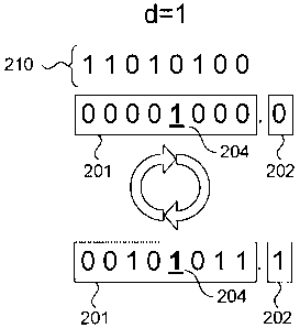
of Figure 5 has
defective cell 204 permanently set to a "1" logic state (d=1), and program
data 210 received
-9-
CA 02708593 2010-07-26
by the memory device is to be stored in data cell group 201. Counting from the
right side of
data cell group 201, defective cell 204 is bit position 4 while bit position 4
of program data
210 is a logic "0". In order to reliably store program data 210 in data cell
group 201, and due
to the mismatch between bit position 4 of the data cell group 201 and bit
position 4 of the
program data 210, all bits of the data which includes program data 210 and the
inversion
status bit are inverted. The inversion process is illustrated by the circular
arrows, and the
resulting data stored by data cell group 201 is shown at the bottom of Figure
6A. Because
the data cell group 201 stores inverted program data, the inversion status
cell 202 is
programmed to a "1" logic state. This "true" logic state indicates that the
data stored in data
cell group 201 is inverted relative to its original version. The data stored
in the inversion
status cell 202 is referred to as an inversion status bit, which is used later
during a read
operation whereby the data is re-inverted back to its original state.
Therefore, by storing an
inverted version of the received program data in the data cell group 201, the
defective cell
204 is reclaimed thereby allowing data cell group 201 to be used even though
it has a
detective cell 204.
[0029] Figure 6B shows an example where different program data 212 is to be
programmed
to data cell group 201 shown in Figure 6A. In this example, bit position 4 of
the program data
and bit position 4 of the data cell group 201 are both logic "1 ", and
therefore match. No
inversion of program data 212 is required, and the program data is directly
stored in data cell
group 201 as shown by the straight arrow. Figure 6C shows an example where the
defective
cell 204 is set to a logic "0". It is assumed that the bit position 4 of data
cell group 201 is
known to have the defective cell set to logic "0". Since bit position 4 of
program data 214 is a
logic "1", there is a mismatch. Accordingly, all bits of program data 214 is
inverted and stored
in data cell group 201 while inversion status cell 202 is programmed to a
logic "1" to indicate
that the corresponding data cell group 201 stores inverted program data.
[0030] Now that the redundancy concept of the present invention has been
described,
following is a description of a memory device or memory macro having the
presently
described redundancy scheme. Subsequent reference to a memory device should be
understood to include a memory macro. A memory macro is an instance of the
memory
circuits which can be integrated into an embedded chip or system. Figure 7 is
a block
diagram of a memory having a redundancy system, according to a present
embodiment. The
memory can be any non-volatile memory, but is now described within the context
of an OTP
memory. The memory device 300 includes an OTP memory array 302, sense
amplifier and
-10-
CA 02708593 2010-07-26
column select circuitry 304, a data register 306 and databus drivers 308. The
data register
306 includes individual self-inverting (SI) data register 310. Each self-
inverting data register
310 corresponds to one cell group, such as the n-bit +1 cell group 200 shown
in Figures 5
and 6A, 6B and 6C.
[0031] The OTP memory array 302 includes bitlines and wordlines connected to
OTP
memory cells, such as the OTP anti-fuse transistor device 100 shown in Figures
4A and 4B.
The bitlines are sensed by sense amplifier circuits in sense amplifier and
column select
circuitry 304, which can include column select circuits for multiplexing one
of a multiple of
bitlines to one sense amplifier circuit, as is well known in the art. Each
sense amplifier circuit
of sense amplifier and column select circuitry 304 provides 1 bit of sensed
read data for
storage by latch circuits in SI data register 310. In the present example,
each of the sense
amplifier circuits also receives 1 bit of program data from latch circuits in
SI data register 310.
In Figure 7, each sense amplifier circuit provides 1 bit of read data and
receives 1 bit of
program data via a pair of SA lines, where each pair is shown as single line
SA. In the
present example configuration, each SI data register 310 receives SA1 to SAn,
where n
corresponds to the size of the n-bit data cell group 201. There can be up to m
SI data
registers 310, where m is an integer value. Each SI data register 310 further
receives and
provides an inversion status bit INV. As previously mentioned, each SI data
register 310
corresponds to an n-bit +1 cell group. As will be described in further detail
later, each SI data
register 310 can invert all the bits of its received program data in the event
the
aforementioned mismatch condition is detected for programming, and can re-
invert all the
read data bits in response to the inversion status bit INV in a read
operation.
[0032] Each SI data register 310 receives program data from a write databus
(not shown)
and provides read data via datalines DL1 to DLn. It is noted that input and
output datalines
for 1 bit are represented by a single dataline. The databus drivers 308
perform a well known
function of driving a databus DB[1:y], where y<=mxn. The width of DB depends
on the
configuration of memory device 300. Additional multiplexing circuitry can be
included within
the block of databus drivers 308 for coupling any set of datalines DL1 to DLn
if the width of
DB is less than mxn. According to the present embodiments, the inversion
status bit INV is
local to an SI data register 310 and the memory array, and is therefore not
output in a
manner similar to read data, nor is it received in a manner similar to program
data.
[0033] Figure 8 is a schematic of a portion of memory array 302 of Figure 7
and its
associated bitline sensing circuitry located in sense amplifier and column
select circuitry
- 11 -
CA 02708593 2010-07-26
block 304. In the present example, memory array 302 is organized in a folded
bitline
architecture, which is well known in the art. In order to simplify the
schematic, only one folded
bitline pair BL/BL* and two wordlines are shown. Column decoder circuitry is
not shown for
selectively coupling multiple folded bitline pairs to the bitline sense
amplifier circuitry in order
to simplify the schematic. Folded bitline memory array 400 includes wordlines
WLO and WL1
connected to the gate terminals of OTP memory cells, implemented in the
present example
as n-channel anti-fuse transistors 402 and 404, n-channel isolation
transistors 406 and 408
for coupling the upper portion of the bitlines to the lower portion of the
bitlines in response to
signal ISO, and bitline sensing circuitry. The bitline sensing circuitry
includes a precharge
circuit 410, a reference charge circuit 412, and a bitline sense amplifier
414.
[0034] The precharge circuit 410 includes two n-channel precharge transistors
416 and 418
connected in series between BL and BL* and having their gate terminals
connected to
precharge signal BLPCH. The shared source/drain terminal of precharge
transistors 416 and
418 receives a precharge voltage VPCH. In operation, both precharge
transistors 416 and
418 will turn on to precharge bitlines BL and BL* to VPCH in response to an
active high logic
level of BLPCH, in preparation for a read operation.
[0035] The reference charge circuit 412 includes n-channel steering
transistors 420 and 422
connected in series between BL and BL*, a capacitance circuit implemented as
an n-channel
transistor 424, and a p-channel precharge transistor 426. Steering transistor
420 has its gate
terminal connected to even selection signal E_REF, while steering transistor
422 has its gate
terminal connected to odd selection signal O_REF. Capacitance circuit 424 has
its gate
terminal connected to voltage supply VCC, and is connected in series with
precharge
transistor 426 between the shared source/drain terminal of steering
transistors 420 and 422
and voltage supply VCC. Precharge transistor 426 has its gate terminal
connected to a
precharge or enable signal PCH*. Generally, capacitance circuit 424 will be
precharged
when a low logic level PCH* pulse is received. The duration of the PCH* pulse
can be
predetermined based on the size of transistor 424 and the desired reference
charge to be
provided. Once precharged, either steering transistor 420 or 422 is turned on
to couple the
reference charge of capacitance circuit 424 to the corresponding bitline. By
example, the
charge being added to a bitline can be approximately 50 millivolts. It is
noted that signals
E_REF and O_REF can be controlled by the same even/odd addressing bit used for
selecting WLO or WL1. In one embodiment, activation of WLO will cause E REF to
be
activated, thereby coupling the reference charge to the complementary bitline.
-12-
CA 02708593 2010-07-26
[0036] The bitline sense amplifier 414 consists of a standard cross-coupled
inverter circuit
which is well known in the art. The circuit includes p-channel transistors
both connected in
series to respective n-channel transistors. The common drain terminal of the p-
channel
transistors receives a high logic level enable signal H_EN, while the common
source terminal
of the n-channel transistors receives a low logic level enable signal L_EN.
H_EN can be a
lowered internal VCC level, while L_EN can be a VSS level. The operation of
bitline sense
amplifier 414 in the DRAM art is well known. When enable signals H_EN and LEN
are
activated, either at the same time or at different times, bitline sense
amplifier 414 will sense a
small voltage differential between BL and BL*, and quickly drive both BL and
BL* to the full
logic level states of H_EN and LEN.
[0037] Because bitline sense amplifier 414 is connected to both bitlines BL
and BL*, the
logic state being programmed or read from the memory array will depend on the
memory cell
that is accessed. For example, if both anti-fuse transistors 402 and 404 store
a logic "1",
bitline sense amplifier 414 will latch two different logic states depending on
which anti-fuse
transistor is accessed. Therefore, a data state corrector 428 is used for
ensuring that the
voltage level corresponding to logic "1" and "0" states is read and
programmed. In the
present example, if WLO is activated to read anti-fuse transistor 404, then
signal EVEN will
be at the logic state for coupling BL* to gating transistor 430. Alternately,
of WL1 is activated
to read anti-fuse transistor 402, then signal EVEN will be at the opposite
logic state for
coupling BL to gating transistor 430. The operation of data state corrector
428 is similar when
program data is to be coupled to either BL or BL* from gating transistor 432.
Data state
corrector 428 can be implemented as a simple bi-directional multiplexor
controlled by signal
EVEN, which can be related to the address used to select wordline WLO and WL1.
Signal
EVEN can be related to signals E_REF and O_REF as well. Data to be programmed
to the
bitlines is provided through n-channel gating transistor 432 which is coupled
to SAi_in and
controlled by program signal PGM. Data to be read from the bitlines is
provided through n-
channel gating transistor 430 which is coupled to SAi out and controlled by
read signal
READ. It is noted that signals SAi_in and SAi_out correspond to the previously
discussed
pair of SA lines. Accordingly, gating transistor 432 is turned on during a
program operation
while gating transistor 430 is turned on during a read operation. Variable "i"
is an integer
value between 1 and max number n.
[0038] The memory array architecture and circuits of Figure 8 is one example
of a non-
volatile memory array configuration which can be used in the embodiments of
the present
-13-
CA 02708593 2010-07-26
invention, and the presently described redundancy scheme is not limited to the
memory array
configuration of Figure 8. The memory array architecture of Figure 8, and in
particular the
configuration whereby separate sense amplifier input and output paths SAi_in
and SAi_out,
facilitates the design and operation of the self-inverting register circuits.
[0039] Figure 9 is a block diagram showing one SI data register 310 of Figure
7 according to
a present embodiment. SI data register 500 includes one SI register cell 502
for each bit of
data to be programmed or read out from memory array 302, and an SI register
cell 504 for
the inversion status bit. The SI register cells 502 are labeled Cell 1 to Cell
n, to correspond to
the n-bit data cell group 201. As shown in Figure 9, each SI register cell 502
provides 1 bit of
program data via an SAi_in line to a sense amplifier and receives 1 bit of
read data via an
SAi_out line (where i=1 to n) from the sense amplifier. The 1 bit of program
data is provided
by a DLi_in line, while the 1 bit of read data is output from the register
cell by a DLi_out line.
[0040] As part of a program operation, each SI register cell 502 is configured
to compare the
logic state of its received program data bit against the logic state of the
cell it is to be
programmed to. In the previously discussed example, a cell set to a logic "1"
is a leaky
defective cell. In the case of a mismatch, a mismatch flag DEFECT is provided
and cascaded
through the SI register cells. In otherwords, each SI register cell 502
logically OR's its
mismatch flag result to that provided by a previous SI register cell 502. The
final DEFECT
flag indicates if one of the SI register cells 502 reported a mismatch, and is
received by SI
register cell 504 which checks to see if the inversion status cell is
defective or not. If one SI
register cell 502 reports a mismatch or SI register cell 504 reports that the
inversion status
cell is defective, then a program inversion signal PGM_INV provided by SI
register cell 504 is
set to an active logic level. All SI register cells 502 receive PGM_INV, and
are configured to
invert their program data bits in response to the active logic level of
PGM_INV. Then the
inverted program data is programmed into the corresponding cells of the data
cell group. In
the present example, the inverted program data is provided to the sense
amplifier circuit via
respective SAi_in lines. Also, the inversion status bit is set and the
corresponding inversion
status cell is programmed to indicate that the program data has been inverted.
[0041] In a read operation, the all SI register cells 502 receive read data
from its respective
SAi_out line, and SI register cell 504 receives the logic state of the
inversion status bit read
from the corresponding inversion status cell. If the inversion status bit is
at a logic level
indicating that the program data has been inverted, then read inversion signal
RD_INV is set
to an active logic level. All SI register cells 502 receive RD_INV, and are
configured to invert
-14-
CA 02708593 2010-07-26
their read data bits in response to the active logic level of RD_INV.
Therefore the original
program data is restored and output to the databus drivers. Accordingly, the
SI register cells
502 and 504 can invert either the program data bits or read data bits within
the register cell
itself.
[0042] Figure 10 is a circuit schematic of the SI register cell 502 shown in
Figure 9,
according to a present embodiment. It is noted that SI register cell 600
includes many of the
same circuits as the dual function shift register circuit disclosed in PAT
3672W-90. In order to
simplify the schematic several circuits are intentionally omitted.
[0043] SI register cell 600 includes a data storage circuit 602, an auto-
program inhibit circuit
604, a program data inversion circuit 606, a read data inversion circuit 608
and data
mismatch comparison logic 610. It is recalled that variable "i" in the signal
names denotes the
specific register cell it is associated with.
[0044] Data storage circuit 602 is responsible for data input, output and
latching operations.
Data storage circuit 602 includes a master latch 612 and a slave latch 614
connected as a
master-slave flip-flop, transfer gating device 616, and an input gating device
618. Latches
612 and 614 can be implemented as simple cross-coupled inverter circuits with
a non-
inverting output relative to its input, but slave latch 614 is configured to
be overwritten by
master latch 612. Those skilled in the art will understand that transistor
sizing can be
configured to achieve this desired function. Gating device 616 is shown as an
n-channel
transistor, but can be replaced with a transmission gate or a p-channel
transistor. Gating
device 616 has its gate terminal connected to clock signal CK, which is a
controlled clock
signal to shift data serially from the master latch 612 to slave latch 614.
Input data DLi_in is
provided to the input of master latch 612 via gating device 618 when signal
WRITE is at the
active logic level, which in the present example is the high logic level.
Output data DLi_out is
provided from the output of slave latch 614. The output of master latch 612,
typically being
program data, is coupled to a sense amplifier via terminal SAi_in, while read
data from the
sense amplifier is provided from terminal SAi_out and stored by slave latch
614.
[0045] The auto-program inhibit circuit 604 is used to verify if a programming
operation was
successful or not. The auto-program inhibit circuit 604 includes a precharge
device 620 and
a coupling device 622 connected in series between a voltage supply such as VDD
and the
input of master latch 612. Both devices 620 and 622 are shown as being n-
channel
transistors in the present embodiment. The gate of precharge device 620 is
connected to
precharge signal PCH and the gate of coupling device 622 is connected to the
output of
-15-
CA 02708593 2010-07-26
slave latch 614. The selection of the voltage supply depends on the logic
state stored by
master latch 612 for selecting a memory cell to be programmed. For example, if
master latch
612 stores a logic 0 (VSS) to indicate programming of the memory cell
connected to that
bitline, then the voltage supply connected to precharge device 620 will be
VDD. Hence, VDD
is the logic state stored in a master latch 612 for a memory cell that is not
to be programmed,
thereby inhibiting programming of the cell connected to that bitline. The auto-
program inhibit
circuit will therefore change the state of the master latch 612 if the memory
cell was
successfully programmed. In the present example, a successfully programmed
memory cell
will result in slave latch 614 storing a high a logic state in a program
verify read operation
following a program operation. Therefore, when PCH is driven to the high logic
level, VDD is
coupled to the input of master latch 612 to flip its state.
[0046] The program data inversion circuit 606 includes a flip-flop circuit 624
and a coupling
device 626 controlled by an evaluation signal EVAL. Flip-flop circuit 624 has
a D-input
receiving program data latched by master latch 612 (SAi_in), and has a non-
inverting output
(Q) and an inverting output (Q*), where the inverting output is connected to
one terminal of
the coupling device 626. The other terminal of the coupling device 626 is
connected to an
input of master latch 612, while its gate terminal receives EVAL. Flip-flop
circuit 624 latches
the data appearing on its D-input and provides the inverted version thereof on
its inverting
output Q* in response to an active logic state of PGM_INV received at its
clock input.
Therefore, if the program data is to be inverted, PGM_INV is driven to the
active logic level
and EVAL can be pulsed to briefly turn on coupling device 626 to electrically
connect the
inverting output Q* to the input of master latch 612. Therefore the logic
state of master latch
612 is inverted. The pulse duration of EVAL can be selected to be at least
long enough to
ensure that master latch 612 is over-written or flipped.
[0047] The data mismatch comparison logic 610 is used in conjunction with
program data
inversion circuit 606, and includes an AND logic gate 628 and an OR logic gate
630. AND
logic gate 628 has a first input receiving an output of slave latch 614 and a
second input
receiving an output of master latch 612. The purpose of AND logic gate 628 is
to detect the
condition where a logic "0" is to be programmed to a defective cell set to
permanent store a
logic "1". As previously discussed for the present example, a logic "1" stored
in master latch
612 inhibits programming, thereby storing a logic "0" in the selected cell.
However, if the
selected cell has been previously determined to be defective and preset to
store a logic "'I",
then there is a mismatch between the data to be stored and the preset logic
state of the cell.
-16-
CA 02708593 2010-07-26
This mismatch condition is detected by AND logic gate 628 when both master
latch 612 and
slave latch 614 store a logic "1". Therefore AND logic gate 628 outputs a
logic "1" output,
which can be referred to as a local DEFECT flag signal, which is then combined
with a global
DEFECT flag signal DEFECTi-1 provided from a previous SI register cell 502 at
OR logic
gate 630. The output of OR logic gate 630 is the updated global flag signal
DEFECTi that is
provided to the next SI register cell 502, or the SI register cell 504. If SI
register cell 600 is
the first register cell, then its OR logic gate 630 has one input tied to
ground or VSS as there
is no previous SI register cell to report a defect. Later, if DEFECTi is at
the active logic level,
which in the present example is a logic "1", then PGM_INV is set to the active
logic level to
enable inversion of the program data.
[0048] The read data inversion circuit 608 is connected between SAi_out and
the input of
slave latch 614, and includes a selector 632 and an inverter 634. Selector 632
is shown as a
multiplexor having a first input for receiving SAi_out and a second input for
receiving an
output of inverter 634, where inverter 634 has its input connected to SAi_out.
Selector 632
passes data from either its first input or second input, to its output in
response to signal
RD_INV, which functions as a selection signal. In its default inactive logic
state, RD_INV
control selector 632 to pass SAi_out directly to slave latch 614. In its
active logic state, where
the read data is to be inverted, selector 632 passes the output of inverter
634 to slave latch
614. Therefore an inverted version of SAi out is stored in slave latch 614.
[0049] Figure 11 is a circuit schematic of the SI register cell 504 of Figure
9, according to a
present embodiment. SI register cell 700 includes many of the same circuits as
shown for SI
register cell 600 of Figure 10. In particular, circuits 602, 604 and 606 are
the same as those
previously described for SI register cell 600. SI register cell 700 does not
have input gating
device 618 for receiving program data, an output terminal at the output of
slave latch 614 for
providing read data, read data inversion circuit 608, or data mismatch
comparison logic 610.
SI register cell 700 is coupled to bitlines of the memory array and sense
amplifier circuits
which can be configured identically to the circuit of Figure 8.
[0050] Following is a description of the circuits that differ from SI register
cell 600 of Figure
10. Instead of having an input for receiving program data, SI register cell
700 includes a reset
circuit consisting of a transistor device 702 for coupling VDD to the input of
master latch 612
in response to a reset signal RST. Reset signal RST can be a pulsed signal
provided prior
each programming operation to set a default program inhibit state for the
inversion status
cell. SI register cell 700 does not require read data inversion, as the
inversion status bit is not
-17-
CA 02708593 2010-07-26
provided externally to the memory device. The SAi_out line can be used as the
RD_INV
signal, or alternately, the output of slave latch 614 can provide the RD_INV
signal. As
previously described, the inversion status bit being permanently set to or
programmed to a
logic "1" indicates that the original program data stored in the data cell
group 201 has been
inverted due to the presence of a defective bit in the data cell group 201 or
the presence of a
defective inversion status cell.
[0051] Instead of data mismatch comparison logic 610, defect detection logic
704 combines
the global flag DEFECTi-1 from the last SI register cell 502 with an output of
slave latch 614.
Accordingly, if either DEFECTi-1 or the output of slave latch 614 is at the
logic "1" state, then
PGM_INV is set to the active logic "1" state. In the present example, if slave
latch 614 is at
the "1" logic state, it means that the corresponding cell was previously
determined to be
defective, and pre-programmed to a specific logic state. The reclamation of a
defective
inversion status cell is the same as for a normal data storing cell. In the
present embodiment,
defect detection logic 704 includes an OR logic gate 706. In the previously
described
embodiments, those skilled in the art should understand that alternate logic
gates or circuits
can be used to achieve the same desired result, since programmed and
unprogrammed logic
states may be reversed relative to those discussed for the present
embodiments.
[0052] Now that example circuits have been described for implementing the
redundancy
scheme of the present embodiments, following are method embodiments describing
sequences for operating the described memory device and circuits with
redundancy.
[0053] Figure 12 is a flow chart of a general method for operating a memory
device having a
redundancy scheme, according to the present embodiments. The method starts at
800
where defective cells are identified and reclaimed. This step includes
identification of leaky
cells at manufacturing and before end user programming, and by example,
reclamation of
leaky cells behaving as a programmed cell includes pre-programming them to a
permanent
logic "1". Redundancy has been implemented after step 800, such that
previously unusable
cells are prepared for storing user data.
[0054] At step 802, the end user which can also be the manufacturer, programs
data to the
memory array. Cell groups, such as cell group 200, without any defective cells
are
programmed without inversion of the program data bits and the inversion status
bit. Cell
groupings with a defective cell, such as a pre-programmed "1" cell from step
800 may be
inverted depending if the data bit position matches or mismatches the pre-
programmed "1" of
the corresponding defective cell.
-18-
CA 02708593 2010-07-26
[0055] At step 804 a read operation is executed to read data from the memory
array. If the
data is read from a cell group having a defective cell, then the read data is
inverted into its
original program data state for output. Otherwise, the read data is output
without inversion.
Therefore, even though program data may be stored in its inverted state, the
resulting read
data will always correspond to the original program data provided to the
memory device.
[0056] Figures 13A and 13B show a particular embodiment of the method shown in
Figure
12. In the present method, it is assumed that the memory cells are OTP memory
cells such
as those described in the present application. Therefore reference is made to
the circuit
schematics of Figures 10 and 11, which are configured for these OTP memory
cells. The
method starts at step 900 where defective cells are identified using any
suitable test
technique. For example a read operation performed on all the unprogrammed
cells can help
determine if any are "leaky". Since such leaky cells tend to behave as
programmed cells, the
detected defective cells are programmed to store a permanent logic "1" at step
902. This can
be done by entering program data into the data register 306 of Figure 7, as
would be done
for a normal programming operation. However, this pre-programming of defective
cells would
typically be performed before shipping to end users for normal use and
operation.
[0057] Steps 900 and 902 would be executed in step 800 of Figure 12. It is
assumed that the
memory device is ready for normal operation. Program data for a data cell
group is provided
to the SI register cells 502 of Figure 9 via the DL1_in to DLn_in lines, and
is thus stored in
the master latch 612. At step 904, a read operation is executed for the cells
to which the
program data is intended to be programmed into. This data is stored in the
slave latch 614 of
Figure 10, and each SI register cell 502 compares its slave latch data to its
corresponding
program data bit stored in master latch 612 using data mismatch comparison
logic 610.
[0058] At step 906, assuming that one cell is defective (logic 1"), and the
corresponding
master latch 612 stores a logic 1", a mismatch is detected between the
permanent logic
state of the inversion status cell and the program data bit. In this case, the
method proceeds
to step 908 where all the program data bits are inverted. This is done by SI
register cell 504
which asserts the PGM_INV signal. In response to PGM_INV, all SI register
cells 502 of the
data cell group clock their respective flip-flops 624. At about the same time,
SI register cell
504 also clocks its respective flip-flop 624 in response to PGM_INV. Signal
EVAL can then
be pulsed to flip the logic state of master latches 612. Hence the program
data of SI register
cells 502, and the reset logic "1" state stored by master latch 612 of SI
register cell 504 is
flipped to a logic "0". As part of step 908, and after the EVAL signal has
been pulsed, the
-19-
CA 02708593 2010-07-26
PCH signal can be pulsed. This will re-invert the master latch 612 of the SI
register cell 502
from the inverted logic "0" back to a logic "1" since coupling device 622 is
presently turned on
by the "1" logic state of the slave latch corresponding to the defective cell.
Since the
defective cell is already programmed, there is no need to reprogram it again.
At steps 910
and 912, the cells are programmed according to the data stored in the mater
latches 612 of
SI register cells 502 and 504.
[0059] Returning to step 906, if there is no mismatch between any of the data
bits and the
defective cell, or there is no defective cell in the cell group, then the data
is programmed at
step 914 without any program data inversion. Also, the inversion status bit
remains
unprogrammed. Steps 904, 908 to 912 or 914 are repeatedly executed for program
operations. After programming, a read operation can be executed, which starts
in Figure
13B.
[0060] At step 916, it is assumed that the bitlines have been precharged and a
wordline has
been asserted for reading data from at least one cell group. The bitlines are
sensed by bitline
sense amplifier circuitry, and sensed bitline data is output. In the present
embodiments, this
sensed bitline data is provided to SI register cell 600 via the SAi_out line.
Because the
inversion status cell is connected to the same wordline as the cells of the
present data cell
group, the inversion status bit is read at substantially the same time at step
918. In SI
register cell 700, the sensed inversion status bit is provided by the SAd_out
line. If at step
920 the inversion status bit (ISB) is true, ie. a logic "1" for example,
indicating that the data of
the data cell group has been inverted relative to the original program data,
then the method
proceeds to step 922. At step 922, RD_INV is at the active logic level to
control selector 632
of each SI register cell 600 to pass the output of inverter 630. Now the slave
latches 614
store the original received program data (inverted read data), which can then
be output from
the memory device via DLi_out at step 924. Returning to step 920, if the
inversion status bit
is false, ie. a logic "0" for example, then the selectors 632 of each SI
register cell 600 couple
SAi_out directly to slave latches 614. The read data is then output via the
DL_out lines in
their uninverted form at step 926.
[0061] Figure 14 is a table showing example memory array cell groups 200,
program data to
be stored in each data cell group 201, and the final stored values in the
respective cell
groups 200 when the cell groups do not have a defective cell or have one
defective cell.
Starting from the left-most column in Figure 14, different program data are
shown in each
row. The second column shows rows of data cell groups 201 and their
corresponding
-20-
CA 02708593 2010-07-26
inversion status cell 202 after testing. Each row of program data is intended
to be stored in a
corresponding row of a data cell group. The testing shows that cells marked
with an "x" are
defective. It is noted that a status inversion cell 202 can be defective. In
the present example,
it is assumed that the test identifies leaky cells. The third column shows the
status of the cell
groups 200 of the same row after the defective leaky cells are programmed to a
logic "1"
state. The fourth column shows the final state of the programmed data of the
row, stored in
the cell group.
[0062] In Figure 14, one inversion status cell 202 is used for each n-bit data
cell group 201.
Figure 15 is a table showing an alternate configuration where two inversion
status cells can
be used for respective segments of an n-bit data cell group of the cell group
200. Figure 15 is
a table similar to the one shown in Figure 14, except that now each row of
program data
consists of two segments, each being 8-bits in length. The corresponding data
cell group 201
of the row in the adjacent column is visually divided into two 8-bit segments,
and has two
inversion status cells 202a and 202b. In the present example, inversion status
cell 202a is
associated with the left-most 8-bits of the data cell group 201, while
inversion status cell
202b is associated with the right-most 8-bits of the data cell group 201.
Accordingly, each
segment can store inverted program data independently of the other.
[0063] The addition of further inversion status cells enables the correction
of multiple cells.
For example, in a row with 32 bits, each 8 bits of the 32 bits can be assigned
one inversion
status cell to correct one defective cell per 8 bits, thus correcting up to 4
defective cells per
row. The distribution of the data segments in an entry can also be varied to
optimize the
method. For example the data segment can be contiguous, or distributed. For
example one
inversion status bit can be assigned for even data bits and another for odd
data bits. The
distribution of the data segments affects the distribution of the defective
cells that can be
corrected. For example for an NVM of 32 bits with 2 redundancy bits (one
redundancy bit per
16 data bits). If the data segments are contiguous, one defective cell can be
corrected in the
first or second 16-bit segments. If the data segments are on even and odd
rows, one
defective cell in even or odd bits can be corrected.
[0064] The previously described embodiments show a redundancy technique to
reclaim and
reuse a defective, leaky cell. The presently described redundancy technique
can be applied
to reclaim and reuse a defective, weak cell. In contrast to the presently
described leaky cell,
a weak cell is one that is logically biased to a logic "0" as it has been
found difficult to
program. The principles of the present redundancy scheme applies to such cells
when they
-21 -
CA 02708593 2010-07-26
have been detected in a cell group 200. The following method can be a modified
version of
steps 906, 908, 910 and 912 of Figure 13A. It is first assumed that the
programming
operation of the memory device is reversible. Since multiple bits are to be
programmed at the
same time, it is possible that while one cell of the cell group 200 programs
its logic "1" state,
another cell cannot program its logic "1" state. Using logic circuits in the
dual shift register of
PAT 3672W-90, a program fail condition can be detected where the cell cannot
be
programmed after a number of preset programming iterations have been
attempted.
Because the auto-program inhibit circuit 604 of the SI register cell 600 can
be used to flip the
logic state stored in master latch 612 after the corresponding cell has been
properly
programmed, the only master latch 612 of the cell group 200 which has not
successfully
programmed after the preset programming iterations will have a logic "0"
stored therein. Cells
for which no programming was intended will have a logic "1" stored in the
corresponding
master latch 612.
[0065] Since it is now known that a cell cannot be programmed (therefore
weak), a program
bit thus mismatches the permanent state of the failed cell, which corresponds
to step 906 of
Figure 13A. In modified step 908, the programming of the cell group 200 is
reversed to their
default states and new program data being an inversion of the original program
data is
loaded into the SI register cells 600. At modified step 910 the inverted data
is programmed
and at modified step 912 the inversion status bit is programmed to indicate
the presence of
inverted program data in the corresponding data cell group. Therefore, the
cell which failed to
program a logic "1" now stores a logic "0".
[0066] Alternately, data having a bit position matching the biased logic state
of the weak cell
can be found for programming to the cell group 200 without any inversion after
the failed
programming condition is identified. In this process, the data stored in the
master latches 612
are shifted to the slave latches 614, and output on the DLi_out lines to
identify the bit position
where programming failed. Once the bit position of the failed programming
operation is
identified, any programming of the cell group 200 is reversed and suitable
program data is
loaded into the SI register cells 502 for programming. Accordingly, while
leaky cells are
identified during testing prior to use, weak cells are identified during an in-
use programming
operation.
[0067] Figure 16 is a table illustrating the presently described redundancy
technique for
reclaiming both weak cells and leaky cells, according to a present embodiment.
Starting from
the left-most side of the table, the first column lists rows of different
program data. The
-22-
CA 02708593 2010-07-26
second column lists corresponding cell groups 200 having detected leaky cells
marked with
an "x". The third column lists the same cell groups 200 shown in rows of the
second column,
but having weak cells detected during a programming operation. The weak cells
are marked
with a "y". The fourth column shows the final programmed data in the cell
groups 200, where
some program data is inverted if the data bit mismatches the preset permanent
logic state of
the corresponding cell in the cell group 200. For those data cell groups 201
which store
inverted program data, its corresponding inversion status cell 202 is
programmed.
[0068] Looking at the program data bits from left to right, if the first bit
position from the left is
to be programmed to a logic "'I", which corresponds to the bit position in the
entry marked
with a "y". As shown in right-most column, the entries are inverted when the
data values
starting with a "1" match the "y" position entry. Therefore when inverted, the
"y" bit stores a
logic "0", and the redundancy bit is programmed to the logic "1" state to
indicate the inverted
status of the stored data. It is noted that the same inversion status bit can
be used for both
types of errors.
[0069] The embodiments of the present invention can be used with any
programmable non-
volatile memory, where defective cells exhibit biased logic states. The
previously described
embodiments of the self-inverting data register 310 is one means for
performing defective
cell detection, program data inversion and read data inversion. Alternate
techniques and
circuits can be developed for obtaining the same desired result.
[0070] In the preceding description, for purposes of explanation, numerous
details are set
forth in order to provide a thorough understanding of the embodiments of the
invention.
However, it will be apparent to one skilled in the art that these specific
details are not
required in order to practice the invention. In other instances, well-known
electrical structures
and circuits are shown in block diagram form in order not to obscure the
invention. For
example, specific details are not provided as to whether the embodiments of
the invention
described herein are implemented as a software routine, hardware circuit,
firmware, or a
combination thereof.
[0071] The above-described embodiments of the invention are intended to be
examples
only. Alterations, modifications and variations can be effected to the
particular embodiments
by those of skill in the art without departing from the scope of the
invention, which is defined
solely by the claims appended hereto.
-23-