Note : Les descriptions sont présentées dans la langue officielle dans laquelle elles ont été soumises.
CA 02708767 2010-06-10
WO 2009/075888
PCT/US2008/013665
COUPLING BETWEEN FREE SPACE AND OPTICAL WAVEGUIDE USING
ETCHED COUPLING SURFACES
Cross-Reference to Related Applications
This application claims the benefit of US Provisional Application No.
61/007,394
filed December 12, 2007 and US Provisional Application No. 61/062,923 filed
January
30, 2008.
Technical Field
The present invention relates to an arrangement for coupling into and out of
an
optical waveguide and, more particularly, to the utilization of etched
coupling facets
along an optical waveguide endface.
Background of the Invention
Coupling light into (and/or out of) an optical waveguide is a key requirement
for
any optical or opto-electronic integrated circuit arrangement. Several
approaches
commonly used in the art include, for example, grating couplers, prism
couplers and
"end-fire" couplers (i.e., coupling into an optical facet along an endface of
an optical
substrate). End-fire coupling, for example, into a nanotaper structure formed
on an
optical substrate offers advantages of simplicity, wide bandwidth of operation
and
(potentially) polarization independent operation. See, for example, an article
entitled
"Nanotaper for compact mode conversion" by V. R. Almeida et al., appearing in
Optics
Letters, Vol. 28, No. 15, August 1,2003.
One remaining difficulty with end-fire coupling, however, is the need for
facet
preparation of the waveguide at the endface of the optical substrate. In order
to
maximize coupling efficiency between a free space signal and the waveguide,
the
endface facet of the waveguide substrate should be as smooth as possible
(i.e., "optically
smooth") so as to limit the effects of scattering and reflections. In most
conventional
systems, optical polishing and/or cleaving operations are used to create the
waveguide
endface facet. Facet polishing, however, is a time consuming process that is
not
considered to be readily compatible with low-cost, wafer-scale production. The
cleaving
process has its own limitations, primarily associated with cleaving a
crystalline material
with the crystal cleavage planes required for the input/output coupling
locations.
1
CA 02708767 2010-06-10
WO 2009/075888
PCT/US2008/013665
Thus, a need remains in the art for providing optically smooth coupling facets
in
a manner that is compatible with low-cost, wafer-scale production.
Summary of the Invention
The need remaining in the prior art is addressed by the present invention
which
relates to an arrangement for coupling into and out of an optical waveguide
and, more
particularly, to the utilization of etched coupling facets along an optical
waveguide
endface.
In accordance with the present invention, a plasma-based etching process is
used
to specifically shape the endface of the optical substrate supporting the
optical
waveguide into a contoured facet which will improve coupling efficiency. The
ability to
use standard photolithographic techniques to pattern and etch the optical
endface facet
allows for virtually any desired facet geometry to be formed ¨ and replicated
across the
surface of a wafer for the entire group of assemblies being fabricated.
In one embodiment, a precisely curved contour is etched into the substrate
endface using a properly-defined photolithographic mask so as to create a
"lens"
coupling feature, with the focal point of the lens selected with respect to
the parameters
of the optical waveguide and the propagating free space signal. By virtue of
using an
etched-based fabrication process, multiple "lens" elements may be formed and
used in a
compound configuration. Alternatively, an angled facet may be formed along the
endface, with the angle sufficient to re-direct reflected/scattered signals
away from the
optical axis. Advantageously, the use of an etch process to form the angled
facet (as
compared to prior art polishing/cleaving) provides improved control and
accuracy of the
angle created with respect to the plane of the endface. Specifically, the
limitations
associated with cleaving along only well-defined crystallographic planes is
eliminated by
using an etch process in accordance with the present invention.
It is an advantage of the present invention that the use of an etching
technique to
prepare the coupling facet allows for a plurality of coupling facets to be
simultaneously
formed for an array of waveguides formed along a substrate surface. Indeed,
the
patterning and etching processes allow for precise alignment between each
waveguide
endface and its associated coupling facet to be achieved.
It is an aspect of the present invention that the use of plasma etching in
facet
preparation allows for wafer-scale processing to be used. That is, the entire
wafer (or a
2
CA 02708767 2010-06-10
WO 2009/075888
PCT/US2008/013665
portion thereof) may be patterned and etched in one step to form a specific
endface
contour for each optical assembly fabricated across the wafer. These facets
will be
essentially uniform, an improvement over using the polishing/cleaving
processes of the
prior art. Moreover, the creation of the optical coupling facets at the wafer
level allows
for wafer-level testing to be performed at reduced cost and complexity when
compared
with prior art processes requiring facet preparation and testing at the
individual
component level.
In a preferred embodiment, the optical substrate is a component of a high
refractive index contrast system, such as an Si/Si02 system ¨ also referred to
in the art as
an SOI-based optical system (the abbreviation "SOI" referring to silicon-on-
insulator).
In this preferred embodiment, it is further considered preferred to have the
endface of the
waveguide pulled back somewhat from the substrate endface, particularly if the
waveguide is formed in a nanotaper geometry. That is, since refractive index
discontinuity between the silicon substrate (n=3.5) and the surrounding
ambient (air,
n=1) is greater than the discontinuity between silicon (n=3.5) and silicon
dioxide
(n=1.5), a larger portion of an incoming free space propagating signal will be
lost by
scattering and reflecting if the waveguide endface is exposed to the ambient.
It is to be
understood, however, that the etched-based facet preparation process of the
present
invention is equally applicable to other silicon-based optical systems, such
as those
utilizing silicon oxynitride or silicon nitride waveguiding arrangements.
The use of a nanotaper configuration is considered to be preferable in that
the
optical mode size is larger and further improves coupling efficiency and
alignment
tolerance with the optical mode. However, the use of a nanotaper is considered
to be
optional and not required for utilization of the etched facet preparation
process of the
present invention.
Other and further advantages and embodiments of the present invention will
become apparent during the course of the following discussion and by reference
to the
accompanying drawings.
Brief Description of the Drawings
Referring now to the drawings,
FIG. 1 is a top view of a conventional prior art "end-fire" nanotaper
waveguide
coupling arrangement;
3
CA 02708767 2010-06-10
WO 2009/075888
PCT/US2008/013665
FIG. 2 is a top view of an exemplary nanotaper waveguide coupling arrangement
=
including an etched coupling facet formed in accordance with the present
invention;
FIG. 3 is a generalized view of an exemplary wafer which may be processed to
form a plurality of etched facets on a plurality of optical structures formed
therein;
FIG. 4 is a graph illustrating the improvement in coupling efficiency between
the
prior art arrangement of FIG. 1 and the inventive structure of FIG. 2;
FIG. 5 contains a top view of an alternative embodiment of the present
invention,
in this case for use with a standard optical waveguide endface (that is, not a
nanotaper
coupler) and comprising a front-to-back angled facet, created with a etching
process;
FIG. 6 is a side view of an alternative angled facet arrangement of the
present
invention, in this case with the angle created in the plane of the substrate
endface;
FIG. 7 is a top view of yet another embodiment of the present invention,
illustrating the formation of an etched curvature along the substrate endface
to form a
lensed coupling facet;
FIG. 8 illustrates a compound lensed coupling facet formed using a pre-defined
pattern and subsequent etch process to create each desired contour along the
optical axis
between the waveguide and substrate endface;
FIG. 9 is a top view of an array embodiment of the present invention, in this
case
with a plurality of curved facets formed with an etch process in a manner
where each
facet is aligned with a separate waveguide within a waveguide array;
FIG. 10 is a top view of a prior art optical system including an off-chip
laser
transmitter and focusing element as used in conjunction with a nanotaper
waveguide
formed on an optical substrate, indicating problems associated with
reflections that will
be re-directed back into the laser component;
FIG. 11 is a top view of an arrangement of an optical system formed in
accordance with present invention where the endface facet of the optical
substrate is
contoured by an etch process to de-focus any reflected signal and direct it
away from the
active region of the laser transmitter;
FIG. 12 is a top view of an alternative optical system of the present
invention,
formed to include an angled facet formed using an etch process to direct a
reflected beam
away from the optical axis; and
FIG. 13 illustrates an alternative embodiment of the configuration of FIG. 11,
in
this case where the nanotaper is angularly disposed to improve coupling
efficiency.
4
CA 02708767 2010-06-10
WO 2009/075888
PCT/US2008/013665
Detailed Description
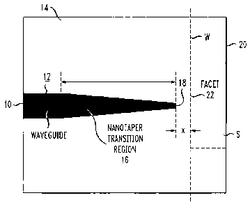
FIG. 1 is a top view of an exemplary optical substrate 1 formed to include an
optical waveguide 2 which also includes a nanotaper transition region 3 and a
nanotaper
tip region 4. It is presumed for the purposes of the present discussion that
optical
substrate 1 is an SOI-based substrate comprising a base layer of silicon (not
shown in
this top view), an overlying dielectric (silicon dioxide) layer 5 (also
referred to as "buried
oxide layer 5" or "BOX layer 5" in the following) and a single crystal, sub-
micron thick
silicon surface layer 6 (also referred to as SOI layer 6).
Using conventional CMOS processing technology, optical waveguide 2 (as well
as adjoining regions 3 and 4) are formed within SOI layer 6. The remainder of
the
exposed surface in this top view is, therefore, BOX layer 5. As mentioned
above, one
prior art technique for preparing nanotaper tip region 4 to receive an optical
signal is to
polish the endface of the optical substrate. In the arrangement of FIG. 1,
this would
require polishing endface 7 of substrate I. Inasmuch as conventional polishing
techniques (such as, for example, chemical-mechanical polishing systems)
cannot control
the endpoint of the polishing process to submicron dimensions, nanotaper tip
region 4
needs to be formed of a predetermined length L to accommodate for this
polishing
inaccuracy. While needing to provide this additional tip region, the prior art
polishing
method also suffers from the scattering and reflection problems discussed
above.
Formation of the endface facet using a prior art cleaving process also suffers
from
drawbacks, particularly related to locating and defining the crystalline plane
used to
create the cleave.
It is to be understood that the prior art illustration of FIG. 1, as well as
the
remaining drawings illustrating the present invention, do not illustrate every
feature of
the final structure (for the sake of clarity). In particular, a dielectric
layer is usually
included as a top, covering layer (referred to as an "interlevel dielectric
layer" or "ILD"
in the art), but is not illustrated so that waveguide 2 is visible in a top
view.
Additionally, it is to be understood that while the prior art arrangement of
FIG. 1 and the
following drawings describe the use of an "S01 structure" and/or "SOI layer",
the etched
coupling facets of the present invention may be used with other material
systems within
which optical waveguides are formed including, but not limited to, silicon
oxynitride
optical waveguides or silicon nitride optical waveguides.
5
CA 02708767 2010-06-10
WO 2009/075888
PCT/US2008/013665
FIG. 2 illustrates an etched facet formed in accordance with the present
invention
to provide coupling between an optical waveguide and a free space optical
signal. An
optical waveguide 10 is shown as formed in an SOI layer 12 of an SOI-based
optical
arrangement (which includes a silicon base layer, not shown, and an overlying
BOX
layer 14). In this particular example, optical waveguide 10 is formed to
include a
nanotaper transition region 16, where as discussed above, the use of a
nanotaper is
beneficial in situations where a larger optical mode size at the coupling
interface is
desired.
In accordance with the present invention and as further shown in FIG. 2, an
etched coupling facet 22 is shown as being formed by removing a portion of BOX
layer
14 from the area between nanotaper transition region 16 and SOI structure
endface 20
(shown as shaded portion S in FIG. 2). More specifically, the waveguide
cladding
material ¨ including both BOX layer 14 and the overlying ILD layer (not shown)
¨ are
removed by the etching process. The remainder of this discussion will thus
refer to the
removal of the "waveguide cladding material", which is understood to include
both BOX
layer 14 and any overlying ILD cladding layer which may be presented. Again,
as
mentioned above, the etched coupling facet of the present invention may be
used with
other types of optical waveguides, such as silicon nitride waveguides or
silicon
oxynitride waveguides.
A conventional patterning technique is used to define the boundaries of shaded
portion S, so that a like area may be removed from each optical assembly
formed across
an entire wafer (see FIG. 3 for a wafer-level illustration, showing a
plurality of patterned
areas to be removed to form coupling facets). Indeed, and as will be discussed
in detail
hereinbelow, the specific geometry (variously referred to also as "contour")
of the region
removed by etching is at the discretion of the user. For example, it is
possible to remove
an entire width of the waveguide cladding material from endface 20 (shown by
the
dotted line "W" in FIG. 2), creating an etched facet endface 22 across the
entire width of
the optical substrate.
In the particular embodiment of the present invention as shown in FIG. 2,
nanotaper transition region 16 is formed to include an endpoint termination 18
(hereinafter referred to as "tip 18") which is disposed at a location which is
pulled back
from etched facet 22 formed in the manner described above.
Several advantages have been discovered when using this pulled back placement
of tip 18 of nanotaper transition region 16. First, when tip 18 is located at
the coupling
6
CA 02708767 2010-06-10
WO 2009/075888
PCT/US2008/013665
facet, it will be exposed to air, which has a lower refractive index than BOX
layer 14.
This difference in refractive index causes an increased portion of the
incoming light
signal to be scattered at tip 18, significantly reducing coupling efficiency
into nanotaper
16. Moreover, as will be discussed in detail hereinbelow, the pulled back
location of
nanotaper tip 18 allows for the facet 22 to be shaped, using standard
photolithographic
patterning and etching processes, to form various facet geometries which will
further
increase coupling efficiency. The thickness "x" of the remaining waveguide
cladding
material beyond tip 18 is also defined by this photolithographic process;
obviously, the
dimensions of the portion removed by the etching process are at the discretion
of the
designer.
A significant benefit of the arrangement of the present invention is that a
plasma
etching process forms an optically smooth surface, limiting the amount of
scattering. As
mentioned above, the use of a "dielectric/air" interface also minimizes the
possibilities of
scattering and reflection. Moreover, a follow-on coating process may be used
to deposit
an anti-reflective material along facet 22; again performed as a wafer-level
process.
FIG. 4 is a graph of insertion loss as a function of nanotaper tip width
(measured
in nm). Curve A is associated with the prior art arrangement of FIG. 1 (where
the
nanotaper tip is exposed at a polished endface of the SOI structure). The
minimum
insertion loss, on the order of 6 dB is associated with a nanotaper tip width
of 200 nm.
As the width either increases or decreases, the loss is seen to increase,
reaching values of
12 dB or more. Curve B is associated with the structure of the present
invention as
illustrated in FIG. 2. As shown, the insertion loss plot is flatter than that
of the prior art
and again exhibits the minimum loss at a tip width of about 200 nm, in this
case having a
value of about 4 dB ¨ a 2dB improvement over the prior art. As the tip width
either
increases or decreases, the loss increases at a slower rate than the prior art
and, in any
case, does not exceed a value greater than about 7 dB.
There are many instances where there is a need to redirect any remaining
reflected signals from re-entering the incoming signal path. As will be
discussed in
detail below in association with FIGs. 10-13, any arrangement which
incorporates a laser
source would benefit from redirecting reflected signals away from the laser
cavity. In
accordance with the present invention, therefore, a plasma etching process may
be used
to particularly angle the coupling facet to re-direct any reflected signals
away from the
active region of the laser source.
7
CA 02708767 2010-06-10
WO 2009/075888
PCT/US2008/013665
FIG. 5 illustrates an exemplary embodiment of the present invention which
provides reflected signal re-direction. FIG. 5 is a top view of the
embodiment,
illustrating the coupling of an optical signal into an endface 11 of optical
waveguide 10;
no nanotaper transition region is utilized in this particular embodiment (it
is to be
understood, however, that any embodiment may or may not include a nanotaper
transition region, at the discretion of the user). As shown, an angled
coupling facet 30 is
created which will successfully re-direct any reflected signal (shown by arrow
"R") out
of the signal path of the incoming optical signal (shown by arrow "I"). In
this particular
embodiment, the angled surface is created from "front to back" along the top
surface of
the substrate. The illustrated angle 0 is selected to be sufficient to ensure
that the
reflected signal will propagate away from angled coupling facet 30, while not
unduly
limiting the coupling efficiency into endface 11 of waveguide 10.
Advantageously, the
use of angled coupling facet 30 also eliminates the need to apply an anti-
reflective (AR)
coating on the facet, saving both fabrication time and expense.
An angled facet may also be formed in the vertical direction, as shown in the
embodiment of FIG. 6. In this case, a downwardly angled facet 32 is formed
using an
etching process in accordance with the present invention. As shown, an
incident ray I
will be directed through the waveguide cladding material and couple into
endface 11 of
optical waveguide 10. Reflected ray R is shown as directed upward at an angle,
away
from the incoming optical axis. In the particular embodiment shown in FIG. 6,
angled
facet 32 is formed at an angle y, controlled by the fabricator for the
intended purpose of
the device.
A significant benefit of using etched coupling facets in accordance with the
present invention is that the contour of the facet may be photolithograph
ically controlled
to create any desired geometry. FIG. 7 is a top view of an exemplary
embodiment of the
present invention illustrating this advantage, where a focusing lens 35 is
formed by
etching a properly-contoured curvature along the endface of the optical
substrate. As
indicated by the arrows, an incoming collimated signal will be focused by lens
35 into
the center portion of optical waveguide 10 at endface I 1. The reciprocal
nature of this
arrangement ¨ as well as every other embodiment of the present invention -
will allow
an outgoing signal propagating along waveguide 10 to be transformed into a
collimated
signal as it exits the optical substrate.
8
CA 02708767 2010-06-10
WO 2009/075888
PCT/US2008/013665
Inasmuch as etching is a process which can be controlled by a
photolithographic
process to create various geometries, it is possible to form multiple
components as a
"coupling facet" between an optical waveguide and a free space optical signal.
FIG. 8 is
a top view of an exemplary multi-component coupling facet, including a set of
etched
contours specifically patterned to form a first, focusing lens 34 and a
second, collimating
lens 36. In this particular embodiment, waveguide 10 is formed to include
nanotaper
transition region 16, terminating at nanotaper tip 18. A cavity 40 is created
through the
waveguide cladding material using a pattern and etch process that is
controlled to create
the necessary contours associated with focusing lens 34 and a first surface 33
of
collimating lens 36. In particular, a photolithographic mask having the
contour of cavity
40 is created on the surface of the waveguide cladding material. Thereafter,
the exposed
area is removed using a suitable etchant, leaving cavity 40 (which will
advantageously
exhibit the desired optically smooth surfaces). Outer surface 37 of
collimating lens 36 is
also contoured using an etch process to provide the desired coupling facet
geometry.
By virtue of using a conventional photolithographic patterning and etching
technique to form coupling facets in accordance with the present invention, a
plurality of
such facets may be formed along a single endface for use with an array of
optical
waveguides. FIG. 9 is a top view of one exemplary array embodiment of the
present
invention, in this case illustrating a plurality of waveguides 10-1, 10-2, 10-
3, ..., 10-N
utilizing a plurality of etched lenses 35-1, 35-2, 35-3, ..., 35-N formed in
the same
manner as the embodiments described above. Advantageously, a single patterning
step
may be used to define the shape and location of the plurality of etched lenses
35-1
through 35-N, providing alignment between the focal point of the lenses and
endfaces
11-1 through 11-N of waveguides 10-1 through 10-N. The ability to replicate
the same
lens geometry across the array is seen to be a significant advantage of the
use of etched
coupling facet preparation in accordance with the present invention. While not
shown, it
is to be understood that an angled facet may be used with an array waveguide
structure
(instead of the illustrated lensed facet). In this case, both the facet angle
and the angle of
the waveguide array with respect to the substrate surface) can be controlled
to provide
optimum coupling (see FIG. 13, below, for an illustration of an angled facet
and an
angled waveguide).
As mentioned above, prior art arrangements for coupling light from a laser
source
into a nanotaper waveguide often encounter stability problems. In many cases,
a
separate micro lens is placed in the optical path between the laser and the
nanotaper.
9
CA 02708767 2010-06-10
WO 2009/075888
PCT/US2008/013665
Unfortunately, both the lens and the nanotaper tip will reflect a portion of
the incoming
laser signal. A significant portion of the reflected signal has been found to
be coupled
back into the active region of the laser, resulting in the instability of the
laser.
FIG. 10 is a top view of a prior art arrangement which exhibits this
instability
problem. As shown, a laser chip 50 including an active region 52 is activated
to emit an
output beam which then propagates through the air and encounters a microlens
element
54 held within a support element 56. Microlens 54 functions to focus the
emitted beam
toward nanotaper tip 18 of waveguide 10, as shown. Inasmuch as prior art
coupling facet
7 is formed by using, for example, a polishing process, a significant portion
of the
incoming beam will be reflected, shown by arrow labeled "Direction of
reflected beam"
in FIG. 10. The on-axis component of this reflected beam will pass unimpeded
through
microlens 54 and re-enter active region 52 of laser 50, as shown.
In accordance with the teachings of the present invention, a coupling facet
having
an etched contour can be formed along the endface of the optical substrate to
minimize
the optical energy directed back into the laser source. In the particular
embodiment of
FIG. 11, the etched coupling facet is shown as exhibiting a contour that will
function as a
lens 60. As discussed above, the patterning of the endface is determined in
conjunction
with the parameters of the waveguide so as to focus the incoming laser beam
into tip 18
of nanotaper 16. Advantageously, the curvature of lens 60 also re-directs any
reflected
portions of the beam away from the optical axis of the system (that is, "de-
focuses" the
reflected beam). The optical design parameters (e.g., focal length) of lens
60, in
combination with the optical parameters of microlens 54, are chosen to
optimize the
coupling of the incident laser beam into nanotaper tip 18 while simultaneously
scattering
the reflected signal away from active region 52.
An alternative laser-based system using a contoured etched facet of the
present
invention is shown in FIG. 12. In this case, an angled facet 62 is formed
along endface
20 of the optical substrate. In this particular embodiment, the angled facet
is formed as
recessed within the optical substrate from endface 20 (in contrast to the
angled facets
illustrated above, which are shown as "notches"; either geometry is suitable
for any
embodiment of the present invention). The angle tv is selected to re-direct
the reflected
signal beyond the capture angle of microlens 54, as shown in FIG. 12. In order
to still
capture a majority of the incoming laser beam, waveguide 10 is formed to be
slightly
offset from the optical axis OA of the system. Improved coupling efficiency
may be
CA 02708767 2015-08-18
found by rotating the disposition of waveguide 10 so as to better align with
the incoming
beam. FIG. 13 illustrates this configuration, where waveguide 10 (and
associated
nanotaper 18) is disposed at an angle of a with respect to optical axis OA.
The scope of the claims should not be limited by the embodiments set forth in
the
examples, but should be given the broadest interpretation consistent with the
description
as a whole.
11