Note : Les descriptions sont présentées dans la langue officielle dans laquelle elles ont été soumises.
CA 02713151 2013-12-10
CA 02713151 2010-07-23
WO 2009/111186 PCT/t3S2009/034721
SEMICONDUCTOR STACK ASSEMBLY HAVING REDUCED THERMAL SPREADING
RESISTANCE AND METHODS OF MAKING SAME
FIELD OF THE INVENTION
One or more aspects of the present invention relate generally to semiconductor
devices and, more particularly, to a semiconductor assembly having reduced
thermal spreading resistance and methods of making the same.
BACKGROUND
As semiconductor technology has advanced, the amount and speed of logic
available on an integrated circuit (IC) has increased. As a result, ICs are
consuming more power. The more power that is consumed, however, the
greater the heat that is generated. Conventionally, ICs include devices such
as
heat sinks to absorb and dissipate heat. A heat sink is an article that
absorbs
and dissipates heat from an IC using thermal contact. For conventional ICs,
heat sinks are thermally coupled to the face side of the die. For flip-chip
mounted ICs, heat sinks are thermally coupled to the backside of the die. Heat
sinks are typically attached to ICs using a thermal paste. The term "face
side"
denotes the side of an IC die that receives the bulk of semiconductor
processing
such that circuitry and interconnect are fabricated on that face side. The
backside is opposite the face side of the die.
For a flip-chip IC, for example, the primary heat removal path is through the
backside of the die, where a heat sink is attached. Heat is dissipated through
several mechanisms, including: (1) vertical heat conduction to the backside of
the die and to the heat sink; (2) vertical heat conduction through the die, as
well
as lateral heat conduction within the base of the heat sink and thermal paste
(i.e., heat spreading); and (3) heat convection to the ambient environment.
Lateral heat conduction in item (2) depends strongly on the ratio between die
area and heat sink base area. When estimating the thermal resistance of a flip-
chip package with a heat sink, engineers must account for the spreading
resistance (a thermal resistance). The higher the ratio between heat sink base
area and die area, the higher the spreading resistance.
The increase in the speed and amount of logic on an IC has outpaced the
CA 02713151 2010-07-23
WO 2009/111186 PCT/US2009/034721
number and performance of input/output (I/O) connections. As a result, IC die
stacking techniques have received renewed interest to address the
interconnection bottleneck of high-performance systems. In stacked IC
applications, two or more ICs are stacked vertically and interconnections are
made between them. One approach to IC stacking involves mounting a second
die on the backside of a first die. The stacked IC arrangement is then flip-
chip
mounted/packaged. A heat sink is then attached to the stacked die or dice.
When a die or dice are stacked on the backside of an IC, the thermal design of
the IC may be compromised. For example, if stacked IC dice occupy a total area
smaller than the area of the primary IC, there are additional components to
spreading resistance. One such component is due to the interface between the
primary IC die and the stacked die or dice. Another such component is due to
the interface between the stacked die or dice and the heat sink. These
additional spreading resistance components lead to poor thermal design and
higher junction-to-package thermal resistance. Accordingly, there exists a
need
in the art for a semiconductor assembly having reduced thermal spreading
resistance and methods of making the same.
SUMMARY
An aspect of the invention relates to a semiconductor device. A first
integrated
circuit (IC) die includes a first surface. At least one additional IC die each
includes a top surface and a bottom surface. The bottom surface of each of the
at least one additional IC die is mounted to the first surface of the first IC
die. At
least one dummy fill each includes a top surface and a bottom surface. The
bottom surface of each of the at least one dummy fill is mounted to the first
surface of the first IC die adjacent the at least one additional IC die. A
mounting
surface is configured for thermal contact with a heat extraction element. The
mounting surface includes the top surface of each of the at least one
additional
IC die and the at least one dummy fill.
Another aspect of the invention relates to a method of fabricating a
semiconductor assembly. A first integrated circuit (IC) die having a first
surface
is fabricated. At least one additional IC die each having a top surface and a
bottom surface is fabricated. The bottom surface of each of the at least one
2
CA 02713151 2010-07-23
WO 2009/111186 PCT/US2009/034721
additional IC die is mounted to the first surface of the first IC die. At
least one
dummy fill each having a top surface and a bottom surface is fabricated. The
bottom surface of each of the at least one dummy fill is mounted to the first
surface of the first IC die adjacent the at least one additional IC die. A
heat
extraction element is mounted to the top surface of each of the at least one
additional IC die and the at least one dummy fill.
Another aspect of the invention is related to a semiconductor assembly. A
semiconductor device includes a primary integrated circuit (IC) die and at
least
one secondary IC die mounted on the primary IC die. A heat extraction element
includes a base mounted to the semiconductor device such that each of the at
least one secondary IC die is between the primary IC die and the heat
extraction
element. At least one dummy fill is adjacent to at least one secondary IC die
and
each thermally couples the primary IC die to the heat extraction element.
BRIEF DESCRIPTION OF THE DRAWINGS
Accompanying drawings show exemplary embodiments in accordance with one
or more aspects of the invention; however, the accompanying drawings should
not be taken to limit the invention to the embodiments shown, but are for
explanation and understanding only.
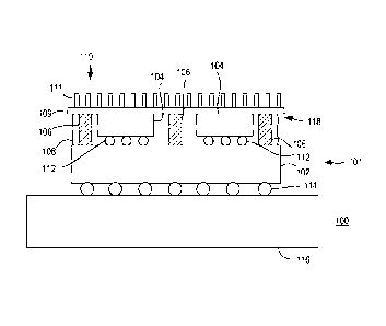
FIG. 1 is a cross-sectional view showing an exemplary embodiment of a
semiconductor assembly in accordance with one or more aspects of the
invention;
FIG. 2 is a cross-sectional view showing an exemplary embodiment of a portion
of a semiconductor device in accordance with one or more aspects of the
invention;
FIG. 3 is a cross-sectional view showing another exemplary embodiment of a
portion of a semiconductor device in accordance with one or more aspects of
the
invention; and
FIG. 4 is a flow diagram depicting an exemplary embodiment of a process of
fabricating a semiconductor assembly in accordance with one or more aspects of
the invention.
3
CA 02713151 2010-07-23
WO 2009/111186 PCT/US2009/034721
DETAILED DESCRIPTION OF THE DRAWINGS
FIG. 1 is a cross-sectional view showing an exemplary embodiment of a
semiconductor assembly 100 in accordance with one or more aspects of the
invention. The semiconductor assembly 100 includes a semiconductor device
101, a heat extraction element 110, and a package substrate 116. The
semiconductor device 101 includes a primary integrated circuit (IC) die 102
(also
generally referred to as a first IC die) and at least one secondary IC die 104
(also
generally referred to as at least one additional IC die). By way of example,
two
secondary IC dice 104 are shown in FIG. 1. The primary IC die 102 includes
circuitry formed on a semiconductor substrate and conductive interconnect
formed over the circuitry (not shown). Likewise, each secondary IC die 104
includes circuitry formed on a semiconductor substrate and conductive
interconnect formed over the circuitry (not shown). The primary IC die 102 and
each secondary IC die 104 may be fabricated using well known IC fabrication
techniques. The primary and secondary IC dice 102 and 104 may comprise any
type of digital, analog, or mixed-signal ICs.
The semiconductor device 101 is mounted on the package substrate 116 via an
array of bump contacts 114. Notably, the array of bump contacts 114 is formed
on a face side of the primary IC die 102. As discussed above, the term "face
side" denotes the side of a die that receives the bulk of semiconductor
processing such that circuitry is fabricated on that face side of the die. The
side
of a die opposite the face side is referred to as the backside of the die. The
bump contacts 114 form an electrical and mechanical connection between the
primary IC die 102 and the package substrate 116. The package substrate 116
may comprise any type of carrier capable of supporting the semiconductor
device 101, such as a printed circuit board (PCB) or the like. Thus, in the
embodiment of FIG. 1, the primary IC die 102 is mounted face-down on the
package substrate 116 in flip-chip fashion.
Each secondary IC die 104 is mounted on the primary IC die 102 such that the
secondary IC die 104 is vertically stacked with the primary IC die 102. In the
present embodiment, each secondary IC die 104 is mounted to the backside of
the primary IC die 102. In general, the surface of the primary IC die 102 upon
which the secondary IC die 104 is mounted is referred to as the first surface
of
4
CA 02713151 2010-07-23
WO 2009/111186 PCT/US2009/034721
the primary IC die 102. Each secondary IC die 104 is mounted on the primary IC
die 102 via bump contacts 112. The bump contacts 112 form an electrical and
mechanical connection between each secondary IC die 104 and the primary IC
die 102. In the present embodiment, each secondary IC die 104 is mounted
face-down in flip-chip fashion. Those skilled in the art will appreciate that
one or
more of the secondary dice 104 may be mounted face-up in conventional
fashion. As is well known in the art, in case of face-up mounting, the bump
contacts 112 are typically replaced with wire bonds extending between the face
side of the secondary die 104 and the backside of the primary die 102.
The semiconductor device 101 includes a mounting surface 118 configured for
thermal contact with the heat extraction element 110. In the present
embodiment, the heat extraction element 110 is shown as a heat sink having a
base 109 and a plurality of fins 111. Those skilled in the art will appreciate
that
such a heat sink is merely exemplary and may have other well-known
configurations. Furthermore, while a heat sink is shown by way of example, it
is
to be understood that the heat extraction element 110 may comprise other types
of elements or combinations of elements, including heat sinks, heat pipes,
and/or
active cooling devices (e.g., air coolers, liquid coolers, etc.). In general,
the heat
extraction element 110 has a base (e.g., the base 109) capable of thermal
contact with the mounting surface 118 of the semiconductor device 101. Such
thermal contact may include a layer of thermal paste (not shown), such as is
well-known in the art.
Each secondary IC die 104 includes opposing top and bottom surfaces. In the
present embodiment, the bottom surface is the face side of the secondary IC
die
104, and the top surface is the backside of the secondary IC die 104. In
embodiments where the secondary IC dice 104 are mounted face-up, the top
and bottom surfaces are reversed, i.e., the top surface is the face side and
the
bottom surface is the backside.
In accordance with one aspect of the invention, the semiconductor assembly 100
includes at least one dummy fill 106. By way of example, three dummy fills 106
are shown in FIG. 1. Each dummy fill 106 includes opposing top and bottom
surfaces. The bottom surface of each dummy fill 106 is mounted to the backside
of the primary IC die 102. The dummy fill(s) 106 is/are adjacent the secondary
CA 02713151 2010-07-23
WO 2009/111186 PCT/US2009/034721
IC die 104. Notably, the primary IC die 102 includes a surface area footprint
defined by the surface area of the backside thereof (generally referred to as
the
first surface area). Likewise, each secondary IC die 104 includes a surface
area
footprint defined by the surface area of the bottom surface thereof.
Collectively,
the secondary IC die 104 provide an aggregate surface area footprint. As
shown, the aggregate surface area footprint of the secondary IC dice 104 is
less
than the surface area footprint of the primary IC die 102. That is, the
secondary
IC dice 104 are mounted in a portion of the surface area of the bottom surface
of
the primary IC die 102. The dummy fill(s) 106 is/are mounted in a second
portion of the surface area of the bottom surface of the primary IC die 102.
That
is, the dummy fill(s) 106 is/are mounted within a portion of the surface area
footprint of the primary IC die 102 that is not occupied by the secondary IC
dice
104. Notably, the dummy fill(s) do not necessarily occupy the remainder of the
surface area footprint of the primary IC die 102. In other words, there may be
some spacing between the secondary IC dice 104 and the dummy fills 106, as
shown in FIG. 1. The dummy fill(s) 106 can be formed of silicon and/or of some
other material, such as a metallic substance.
The height of the dummy fill(s) 106 and the secondary IC dice 104 (i.e., the
distance between top and bottom surfaces) are substantially the same. In this
manner, the top surfaces of the dummy fill(s) 106 and the secondary IC dice
104
form the mounting surface 118. That is, the heat extraction element 110 is in
thermal contact with the top surfaces of the dummy fill(s) 106 and the
secondary
IC dice 104. For example, the heat extraction element 110 may be mounted to
such top surfaces using a thermal paste.
The dummy fill(s) 106 and the secondary IC dice 104 thermally couple the
primary IC die 102 to the heat extraction element 110. In particular, the
dummy
fill(s) 106 provide direct thermal conduction path(s) from the primary IC die
102
to the base 109 of the heat extraction element 110. In addition, the dummy
fill(s)
106 reduce thermal spreading resistance between: (1) the interface between the
secondary IC dice 104 and the heat extraction element 110; and (2) the
interface
between the primary IC die 102 and the secondary IC dice 104. In other words,
the dummy fill(s) 106 reduce junction-to-package thermal resistance in die
stacking applications, as compared to semiconductor devices without such
6
CA 02713151 2010-07-23
WO 2009/111186 PCT/US2009/034721
dummy fill(s) 106.
The dummy fill(s) 106, the secondary IC dice 104, and the primary IC die 102
may be encapsulated by a mold compound 108. The mold compound 108 may
comprise any type of molding compound known in the art used to package ICs.
In some embodiments, the mold compound 108 comprises a cured polymer
resin-based material, thermoplastic material, thermoset material, or the like.
The
mold compound 108 may be filled with the dummy fill(s) 106.
In some embodiments, the dummy fill(s) 106 comprise a high thermal
conductivity material, such as silicon or like type materials having a thermal
conductivity greater than or equal to silicon, including metallic fills (e.g.,
copper,
aluminum, etc.). In specific non-limiting embodiments, the dummy fill(s) 106
comprise dummy silicon fills. In one example, the dummy silicon fills do not
have any active or passive components formed thereon. Such dummy silicon
fills do not require the expense of fabricating circuitry and conductive
interconnect and thus may be manufactured using a lower cost manufacturing
process. For example, the dummy silicon fills can be manufactured and diced
from lower cost wafers as compared to the wafers used for the IC dice (e.g., 6
inch or 8 inch wafers for dummy silicon fills versus 12 inch wafers for IC
dice).
FIG. 2 is a cross-sectional view showing an exemplary embodiment of a portion
of the semiconductor device 101 in accordance with one or more aspects of the
invention. In FIG. 2, a part of the primary IC die 102 is shown with a
secondary
IC die 104 and a dummy fill 106A mounted thereon (one of the dummy fill(s)
106). In the present embodiment, the dummy fill 106A is a dummy silicon fill
having a silicon substrate 202 and a thermal contact 204. The thermal contact
204 may comprise, for example, at least one bump contact or the like. A
thermal
conduction path is established from the primary IC die 102 to the silicon
substrate 202 via the thermal contact 204 and eventually to the heat
extraction
element 110. Other dummy silicon fills may be configured similarly for the
remaining portion of the semiconductor device 101.
FIG. 3 is a cross-sectional view showing another exemplary embodiment of a
portion of the semiconductor device 101 in accordance with one or more aspects
of the invention. In FIG. 3, a part of the primary IC die 102 is shown with a
secondary IC die 104 and a dummy fill 106B mounted thereon (one of the
7
CA 02713151 2010-07-23
WO 2009/111186 PCT/US2009/034721
dummy fill(s) 106). In the present embodiment, the dummy fill 106B is a dummy
silicon fill having a silicon substrate 301. The silicon substrate 301
includes at
least one passive component fabricated thereon. Such a dummy silicon fill is
generally referred to as a specialized dummy silicon fill. In some
embodiments,
circuitry may be formed in the silicon substrate 301 (not shown). A layer of
conductive interconnect 302 may also be formed on the silicon substrate 301.
The conductive interconnect 302 and/or circuitry may be configured to form one
or more passive components 304, such as resistors, capacitors, inductors, or
any combination thereof. These components can be used to facilitate RF/mixed
signal integration, or to act as decoupling capacitors, for example.
The dummy fill 106B is mounted on the primary IC die 102 via contacts 306. The
contacts 306 provide a thermal contact between the primary IC die 102 and the
dummy fill 106B. In addition, the contacts 306 may provide for electrical
communication between the passive component(s) 304 and circuitry in the
primary IC die 102. For example, the primary IC die 102 may include one or
more through die vias (TDVs) 312 coupled to conductive interconnect 310 on the
face side of the primary IC die 102, thereby providing a path between the
passive component(s) 304 and circuitry on the primary substrate 102. The
contacts 306 may also provide for electrical communication between the passive
component(s) 304 and circuitry in the secondary IC die 104. For example, one
or more conductors 308 may be formed on the backside of the primary IC die
102 between the contacts 306 and the bump contacts 112 of the secondary IC
die 104. Other dummy silicon fills may be configured similarly for the
remaining
portion of the semiconductor device 101.
The passive component(s) 304 may be used for various purposes. For example,
the passive component(s) 304 may be used for mixed-signal circuits. Capacitors
may be formed in silicon fills to implement de-coupling capacitors for a power
distribution network. Unlike off-chip capacitors, which are connected to the
package substrate 116 through bond-wires or solder balls, the de-coupling
capacitors in the dummy silicon fills are attached directly to the active
device. As
a result, they have less parasitic resistance and provide superior performance
as
compared to off-chip capacitors. Those skilled in the art will appreciate that
the
passive component(s) 304 may be used for a myriad of other purposes.
8
CA 02713151 2010-07-23
WO 2009/111186 PCT/US2009/034721
FIG. 4 is a flow diagram depicting an exemplary embodiment of a process 400 of
fabricating a semiconductor assembly in accordance with one or more aspects of
the invention. The process 400 begins at step 402, where a primary IC die is
fabricated using well known IC fabrication techniques. In particular, during
IC
fabrication, a wafer of primary IC dice is produced. The wafer may be scored
and strips of a plurality of primary IC dice obtained. Although step 402 is
broadly
described in terms of a single primary IC die, it is to be understood that
multiple
primary IC dice may be produced and processed in parallel using the method
400. That is, the steps of processing a single primary IC die can be extended
to
process multiple primary IC dice. For example, the primary IC dice may be
processed in the steps below a strip at a time.
At step 404, at least one secondary IC die is fabricated for the primary IC
die (or
for each of the primary IC dice in a strip). The secondary IC die or dice may
be
fabricated using similar IC fabrication techniques to the primary IC die. The
secondary IC die or dice may be singulated from wafer(s) after manufacture. At
step 406, the secondary IC die or dice are mounted on the primary IC die (or
on
each of the primary IC dice in a strip). As described above, the bottom
surface
of a secondary IC die is mounted to the backside of a primary IC die. At step
408, at least one dummy fill is fabricated for the primary IC die (or for each
of the
primary IC dice in a strip). At optional step 409, at least one passive
component
is fabricated on each of the dummy fill(s).
At step 410, the dummy fill(s) is/are mounted on the primary IC die (on each
of
the primary IC dice in a strip). As described above, the bottom surface of a
dummy fill is mounted to the backside of a primary IC die. At step 412, the
primary IC die (or strip of primary IC dice) is encapsulated with a mold
compound. As described above, the mold compound encapsulates the primary
IC die, the secondary IC die or dice, and the dummy fill(s) to produce a
composite package. At optional step 414, if a strip of primary IC dice is
being
processed, then the primary IC dice may be singulated to produce individual
composite packages. At step 416, the primary IC die (or primary IC dice) may
be mounted to a package substrate (or multiple package substrates). At step
418, a heat extraction element may be mounted to the composite package (or
each of the composite packages).
9
CA 02713151 2010-07-23
WO 2009/111186 PCT/US2009/034721
While the foregoing describes exemplary embodiments in accordance with one
or more aspects of the present invention, other and further embodiments in
accordance with the one or more aspects of the present invention may be
devised without departing from the scope thereof, which is determined by the
claims that follow and equivalents thereof. Claims listing steps do not imply
any
order of the steps. Trademarks are the property of their respective owners.