Note : Les descriptions sont présentées dans la langue officielle dans laquelle elles ont été soumises.
CA 02713353 2010-07-26
WO 2009/128866 PCT/US2008/088514
RADIO FREQUENCY (RF) INTEGRATED CIRCUIT (IC) PACKAGES WITH
INTEGRATED APERTURE-COUPLED PATCH ANTENNA(S) IN RING
AND/OR OFFSET CAVITIES
Field of the Invention
The present invention generally relates to communications circuitry, and, more
particularly, to radio frequency (RF) integrated circuit (IC) packages.
Background of the Invention
In a wireless network, the connectivity and communication between devices is
achieved through antennas attached to receivers or transmitters, in order to
radiate the
desired signals to or from other elements of the network. In radio
communication
systems, such as millimeter-wave radios, discrete components are usually
assembled with
low integration levels. These systems are often assembled using expensive and
bulky
waveguides and package-level or board-level microstrip structures to
interconnect
semiconductors and their required transmitter- or receiver-antennas. With
recent progress
in semiconductor technology and packaging engineering, the dimensions of these
radio
communication systems have become smaller. For applications such as wireless
universal
serial bus (USB), the operating distance is limited to about a meter; and a
single antenna
with about 7 dBi at 60 GHz will provide the necessary antenna gain. For
distances as
long as 10 meters (such as wireless video) or longer (such as radar), in point-
to-point
applications, antenna gains as high as 30 dBi, depending on the application,
are required.
However, high gain antennas for wireless video applications have very narrow
beam
widths, so pointing the antenna is very difficult for consumers. Therefore, a
radiation
pattern steerable array, such as a phased array, is necessary. Phased arrays
are also widely
used in military radars. However, packaging RF chips with integrated antennas
or phased
arrays is extremely difficult and very expensive due to the expensive
components and
extensive labor involved.
1
CA 02713353 2010-07-26
WO 2009/128866 PCT/US2008/088514
Summary of the Invention
Principles of the present invention provide techniques for implementing RF IC
packages with integrated aperture-coupled patch antennas in, for example, ring
and/or
offset cavities.
In an exemplary embodiment, according to one aspect of the invention, a radio-
frequency integrated circuit chip package with N integrated aperture-coupled
patch
antennas, N being at least two, includes N generally planar patches, and at
least one
generally planar ground plane spaced inwardly from the N generally planar
patches and
substantially parallel thereto. The ground plane is formed with at least N
coupling
aperture slots therein, and the slots are substantially opposed to the
patches. Also
included are N feed lines spaced inwardly from the ground plane and
substantially
parallel thereto, at least one radio frequency chip spaced inwardly from the
feed lines and
coupled to the feed lines and the ground plane, and a first substrate layer
spaced inwardly
from the feed lines. The first substrate layer is formed with a chip-receiving
cavity, and
the chip is located in the chip-receiving cavity. An additional element
includes a second
substrate layer interposed in a region between the ground plane and a plane
defined by
the patch. The patch is formed in a first metal layer, the ground plane is
formed in a
second metal layer, and the second substrate layer defines an antenna cavity.
The N
generally planar patches are located in the antenna cavity.
Optionally, an island is formed in the second substrate layer, within the
cavity,
thus defining a ring shape of the cavity, and the N generally planar patches
are located in
the ring shape. The island is substantially opposed to the chip-receiving
cavity.
In another optional approach, the antenna cavity is spaced away (offset) from
the
chip-receiving cavity when viewed in plan, such that loads incurred during
insertion of
the chip into the chip-receiving cavity are substantially supported away from
the antenna
cavity.
In another aspect, a method of fabricating a radio-frequency integrated
circuit
chip package with N integrated aperture-coupled patch antennas, N being at
least two,
includes the steps of providing a package of the kind described (less the
chip), with the
optional island as described, and inserting at least one radio frequency chip
into the
2
CA 02713353 2010-07-26
WO 2009/128866 PCT/US2008/088514
cavity, with the island supporting loads induced by the insertion of the chip
into the
cavity.
In yet another aspect, a method of fabricating a radio-frequency integrated
circuit
chip package with N integrated aperture-coupled patch antennas, N being at
least two,
includes the steps of providing a package of the kind described (less the
chip), with the
optional offset cavity configuration as described, and inserting at least one
radio
frequency chip into the cavity, such that loads incurred during insertion of
the chip into
the chip-receiving cavity are substantially supported away from the antenna
cavity.
One or more embodiments of the invention are suitable for automatic processes
and reduce the number of components previously involved with packaging
antennas.
These and other objects, features and advantages of the present invention will
become apparent from the following detailed description of illustrative
embodiments
thereof, which is to be read in connection with the accompanying drawings.
Brief Description of the Drawings
FIG. 1 shows an exemplary embodiment of a package, in cross section, according
to an aspect of the invention;
FIG. 2 shows an exemplary embodiment of another package, in cross section,
according to another aspect of the invention;
FIG. 3 shows an exemplary embodiment of yet another package, in cross section,
according to yet another aspect of the invention;
FIG. 4 is a bottom view of an exemplary package with no reflector or an
embedded reflector;
FIG. 5 is a bottom view of an exemplary package with a visible reflector;
FIG. 6 is a bottom view of an exemplary planar phased array embodiment;
FIG. 7 is a top view of a rectangular ring cavity package, according to a
further
aspect of the invention (please note that the terms top view and plan view are
used
interchangeably herein);
FIG. 8 is a cross section taken along line VIII-VIII in FIG. 7;
FIG. 9 is a larger version of the package of FIG. 7;
FIG. 10 is a cross section taken along line X-X in FIG. 9;
3
CA 02713353 2010-07-26
WO 2009/128866 PCT/US2008/088514
FIG. 11 is a top view of a circular ring cavity package, according to yet a
further
aspect of the invention;
FIG. 12 is a cross section taken along line XII-XII in FIG. 11;
FIG. 13 is a smaller version of the package of FIG. 11;
FIG. 14 is a cross section taken along line XIV-XIV in FIG. 13;
FIG. 15 is a top view of an offset (side-by-side) cavity package, according to
a
still further aspect of the invention;
FIG. 16 is a cross section taken along line XVI-XVI in FIG. 15;
FIG. 17 is a top view of an exemplary sixteen antenna phased-array
configuration,
according to an even further aspect of the invention; and
FIG. 18 is a top view of another exemplary sixteen antenna phased-array
configuration, according to an additional aspect of the invention.
Detailed Description of Preferred Embodiments
One or more embodiments of the invention provide an apparatus and method for
low cost packages with integrated antennas and phased arrays operating in the
millimeter
wave (mmWave) range. An exemplary inventive package with integrated antennas
is
based on a multilayer printed circuit board (PCB). The package contains, for
example, a
rectangular or ring cavity for implementing high performance antenna(s) or
antenna
arrays and another cavity housing mmWave radio frequency (RF) integrated
circuit chips.
One or more embodiments of the invention also provide techniques to overcome
the
difficulties in making internal cavities and to avoid the need to employ wire
bond
technology at mmWave frequencies. Embodiments of the inventive packaging
technology are consistent with the PCB manufacturing process and can be used
for
packages with an integrated antenna or antenna array.
Instances of the invention thus provide low cost packaging with integrated
antennas or planar phased arrays; in particular, chip packaging with
integrated antennas
or planar phased array designs for mmWave frequencies and above.
Typical chip packages with integrated antennas have three major parts: (i) an
RF
chip, (ii) one or more antennas, and (iii) a package carrier (and in some
instances, a
package lid or cover, or an encapsulant to protect the package). One or more
4
CA 02713353 2010-07-26
WO 2009/128866 PCT/US2008/088514
embodiments of the invention provide a package that has high performance
antennas, an
interface for flip-chipping an RF chip and an interface for flip-chipping the
package to a
printed circuit mother board.
FIG. 1 shows a cross-sectional view of an exemplary package 100, according to
an aspect of the invention. Note that section lining is omitted throughout the
figures, for
clarity. The package has seven total layers, including substrate and bounding
layers. For
mmWave applications, especially for frequencies above 60 GHz, bounding film
and/or
layer thickness has to be considered in the design process. Given the
teachings herein, a
person having ordinary skill in the antenna and packaging arts will know how
to take the
thickness into account and how to employ high precision PCB fabrication
techniques to
make embodiments of the invention. The package 100 also has a number of metal
layers.
In particular, there is an outermost substrate 102. Immediately inward
therefrom is a
metal layer used for the patch(es) 104 of the patch antenna(s). Inward of the
substrate
102 and patch antenna 104 (only a single antenna is depicted in FIG. 1, but
more can be
provided as discussed below) are a bound film layer 106, another substrate
layer 108, and
another bound film layer 109. Another metal layer, inward of bound film 109,
is used for
the ground plane 110 of the patch antenna. Slot(s) 113 on the ground plane are
used for
the apertures of the aperture-coupled patch antennas. The ground plane 110
also separates
the radiating elements (patches) 104 from the feed line(s) and the RF chip(s),
discussed
below.
Another substrate 112 is inward from ground plane 110. Another metal layer is
inward from substrate 112 and is used to implement the antenna feed line(s)
114, pads
116, 118, 120 for RF chip connections (preferably a flip-chip/C4 ("controlled
collapse
chip connection") type of connection), and interconnection(s) 122 (as
appropriate) to one
or more vias, such as via 124, in a further bound film layer 126 inward of the
metal layer
forming feed line 114, and a further substrate 128 inward of bound film 126. A
still
further metal layer provides all the pads for signal, control, power supply,
and ground
connections to the mother PCB (the mother PCB is omitted from the figure for
clarity).
Pads may include ground pad 130 interconnected with ground plane 110 through
ground
via 140, as well as one or more of signal, power, and control pads exemplified
by pad 132
connected to interconnection 122 and antipad 142 by via 124. The vias may be,
for
5
CA 02713353 2010-07-26
WO 2009/128866 PCT/US2008/088514
example, plated through holes. Package pads 134 may also be provided.
Depending on
the patch antenna design, an optional reflector 144 can also be implemented on
the same
metal layer as the pads 130, 132, 134. In some instances, as discussed below,
the reflector
144 is embedded.
To implement the flip-chip approach, the chip 162 preferably has a plurality
of
solder dots connected directly to the chip connection pads 116, 118, 120.
To enhance the patch antenna bandwidth, patches may be air suspended or
supported with a foam material with a dielectric constant close to one at low
frequency
applications. However, at mmWave frequencies, especially for package
applications, air
suspended or foam supported patches are not realistic. Thus, in one or more
embodiments
of the invention, an air cavity 150 can be implemented in the packages. To
avoid issues
from hot gases during the PCB manufacturing process, vent hole(s) 152 can be
employed.
These holes can be designed such that they have little effect on the antenna
performance.
For example, hole 152 can be located near the middle of the cavity 150 or
close to the
edge of the cavity 150, and can be made relatively small, consistent with
adequate
venting. The vent holes can be on the top (outermost part of) the cavity 150
as shown in
FIG. 1 or on the side of the cavity as discussed below, depending on the
manufacturing
process used.
The ground plane 110 is also used for making ground connections through vias
(e.g., via 140) and signal, power, and control connections through vias and
antipads (e.g.,
via 124 with antipad 142, illustrative of a via with antipad that could be
used for signal,
power, or control functionality). Antipads are beneficial from a manufacturing
standpoint, and result in increased reliability, as it is difficult to achieve
reliability in
partial vias (i.e., vias such as via 124 that do not extend completely through
a structure)
without use of antipads.
An open chip-receiving cavity or socket 160 is realized in the substrate 128
and
bound film 126. This socket is used to hold the RF chip 162. The chip is
attached to the
package through flip-chip bonding.
Note that all the mmWave components (antennas, power amplifiers, low noise
amplifiers, and the like) are in the package 100. Vias 124, 140 are used to
pass through
DC or much lower frequency signals.
6
CA 02713353 2010-07-26
WO 2009/128866 PCT/US2008/088514
The package 100 may advantageously be attached to the mother board (not
shown) through a ball grid array (BGA).
FIG. 2 shows an embodiment 200 substantially similar to embodiment 100 except
that reflector 144 is encapsulated by an additional bound layer 170 inward of
reflector
144 and an additional substrate 172 inward of bound layer 170. Similar items
have
received the same reference number and will not be described again. Chip
receiving
socket 160 is also formed in substrate 172 and bound layer 170 in this
embodiment.
FIG. 3 shows an embodiment 300 substantially similar to embodiment 200 except
that vent 352 runs sideways through layer 108 so as to vent cavity 150.
Similar items
have received the same reference number and will not be described again.
FIG. 4 presents a bottom view 400 where chip 162 is encapsulated with
encapsulant 402. The chip can be partially or completely encapsulated, for
example, for
purposes of resisting humidity. A plurality of outer pads 404 may correspond,
for
example, to attachment, heat conduction, or ground pads such as pad 130, while
a
plurality of inner pads 406 may correspond, for example, to signal, control,
or power pads
such as pad 132. In FIG. 4, there is no reflector or the reflector is
embedded. FIG. 5
shows a view 500 similar to view 400 but of a package with a reflector 144,
such as in
FIG. 1. Similar items have received the same reference number and will not be
described
again.
FIG. 6 shows an exemplary package 600 with a 2x2 planar phased array layout.
It
is possible to have more than two antennas on each row. This basic 2x2 array
can be used
to form much larger arrays. In addition to first antenna patch 104 with first
feed line 114,
also included are second, third and fourth antenna patches 602, 604, 606 with
corresponding second, third and fourth feed lines 608, 610, 612. Each feed
line is
connected to chip 162 as described above. Although, for purposes of
illustrative
convenience, the feed lines are shown ending at the patches in FIG. 6, it will
be
appreciated that they may overlap the corresponding patches when viewed in top
or
bottom plan views, and are spaced from the corresponding patch and coupling
aperture
when viewed in cross-section as shown in FIGS. 1-3 (for example, one end of
the feed
line passes the center of the patch (FIG. 17) or stays at the center (FIG.
18). The other
end of the feed line goes just past the edge of the RF chip).
7
CA 02713353 2010-07-26
WO 2009/128866 PCT/US2008/088514
It will thus be appreciated that aspects of the invention include a package
with a
socket for an RF chip, and a planar antenna. In one or more instances, the RF
chip is flip-
chip attached to the package. Internal cavities can be used to improve the
patch
bandwidth. Venting holes can be used to remove the hot gases during the PCB
manufacturing process. The package can be attached to the mother PCB through a
BGA.
The package can implement a planar phased array.
In view of the discussion of FIGS. 1-6, it will be appreciated that, in
general
terms, an aperture-coupled patch antenna package, according to an aspect of
the
invention, can include at least one generally planar patch, such as patch 104.
Also
included is at least one generally planar ground plane, such as plane 110,
spaced inwardly
from the generally planar patch 104 and substantially parallel thereto. The
ground plane
is formed with at least one coupling aperture slot, such as slot 113, therein.
The slot 113
is substantially opposed to the patch 104. At least one feed line, such as
line 114, is
spaced inwardly from the ground plane 110 and is substantially parallel
thereto. At least
one radio frequency chip, such as chip 162, is spaced inwardly from the feed
line 114 and
is coupled to the feed line 114 and the ground plane 110. Also included is a
first
substrate layer, such as that formed by bound film 126 and substrate 128,
spaced
inwardly from the feed line 114. The first substrate layer is formed with a
chip-receiving
cavity, such as cavity 160. The chip 162 is located in the chip-receiving
cavity 160.
Given the description herein, a person skilled in the PCB and antenna arts can
make embodiments of the invention. Non-limiting examples of materials that may
be
used include thermoset plastic/ceramic/woven glass or similar laminates such
as the
Rogers R04000 series of materials (and other compatible materials) available
from
Rogers Corporation of Rogers, Connecticut USA, as well as copper for metal
layers,
possibly gold-plated on pads or other exposed areas. Similar techniques can be
used for
all the depicted embodiments, including FIGS. 1-18.
It will be appreciated that advantageously, embodiments of the invention, such
as
100, 200, and 300, provide a complete package and not a mere patch antenna
separate
from the chip and other packaging.
Note that vias such as 124, 140 may be formed, for example, using plated
through
holes.
8
CA 02713353 2010-07-26
WO 2009/128866 PCT/US2008/088514
Embodiments of the invention may also include a second substrate layer, such
as
that formed by substrate 108 and bound films 106, 109, interposed in a region
between
the ground plane 110 and a plane defined by the patch 104. The patch 104 may
be
advantageously formed in a first metal layer and the ground plane 110 may be
advantageously formed in a second metal layer.
In one or more embodiments, a third substrate layer, such as that formed by
substrate 112, is interposed in a region between the ground plane 110 and the
feed line
114. The feed line 114 may be advantageously formed in a third metal layer.
Further,
one or more packages in accordance with embodiments of the invention may
include at
least one via, such as via 190, formed in the third substrate layer 112 and
coupled to the
ground plane 110. A plurality of chip connection pads, such as pads 116, 118,
120, can
be formed in the third metal layer. At least one of the chip connection pads,
such as 118,
can be coupled to the at least one via 190 in the third substrate layer. The
chip
connection pads couple the chip to the feed line 114 (pad 120), the via 190
(pad 118) and
the via 124 (pad 116).
One or more embodiments of the invention may include one or more signals pads,
one or more control pads, and one or more power supply pads, all of which are
exemplified by pad 132, as well as one or more ground pads, such as 130. The
signal,
control, power supply and ground pads are advantageously formed in a fourth
metal
layer. As noted, package pads 134 can optionally be provided.
Also included in one or more embodiments is at least one ground via, such as
140,
coupling the ground plane 110 and the ground pad 130. The at least one ground
via 140
passes through the first and third substrate layers (e.g., substrate 112,
bound film 126, and
substrate 128), in a region not intersecting the feed line 114. One or more
embodiments
include at least one each of power, signal, and control antipads, such as
antipad 142,
formed substantially coplanar with the ground plane 110. At least one signal
via couples
the signal antipad and the signal pad, and passes through the first and third
substrate
layers. Similarly, at least one power via couples the power antipad and the
power pad,
and passes through the first and third substrate layers. Furthermore, at least
one control
via couples the control antipad and the control pad, and passes through the
first and third
9
CA 02713353 2010-07-26
WO 2009/128866 PCT/US2008/088514
substrate layers. As noted, pad 132, via 124, and antipad 142 are illustrative
of pad, via,
and antipad elements that may be provided for power, signal, and control
functionality.
As also noted, in some instances, a reflector, such as 144, is spaced inwardly
from
the third substrate layer and is generally opposed to the coupling aperture
slot 113. The
reflector can be located on an inner surface of the first substrate layer
(e.g., inmost
surface of substrate 128). The reflector can be exposed, as in FIG. 1, or
embedded, as in
FIGS. 2 and 3, in which case the package can include a fourth substrate layer,
such as that
formed by bound film 170 and substrate 172, spaced inwardly from the reflector
144.
The reflector can thus be embedded between the first and fourth substrate
layers.
Advantageously, the second substrate layer, such as that formed by films 106,
109
and substrate 108, is formed with an air cavity, such as cavity 150, therein.
Air cavity
150 is located between the patch 104 and the coupling aperture slot 113 in the
ground
plane 110. Preferably, the air cavity is formed in communication with a vent,
such as
vent 152 or 352. In the latter case, as in FIG. 3, the vent 352 is formed in
the second
substrate layer; in particular, in substrate 108. In the former case, vent 152
is formed in
an additional substrate layer, such as that formed by substrate 102, spaced
outwardly
from the patch 104. The patch is formed on the additional substrate layer 102,
and the
vent is formed in the additional substrate layer 102.
As noted with regard to FIG. 6, in one or more embodiments of the invention,
two
or more patches are implemented to form a planar phased array. Thus, in
general terms,
the above-discussed patch 104 may be designated as a first patch, and the
above-
discussed feed line 114 is a first feed line. The ground plane can be formed
with one or
more additional coupling aperture slots, like slot 113. The package can
include one or
more additional generally planar patches, such as patches 602, 604, 606,
spaced
outwardly from the ground plane. The additional slots can be substantially
opposed to
the additional patches. The package can also include one or more additional
feed lines,
such as lines 608, 610, 614, spaced inwardly from the ground plane and
substantially
parallel thereto. The at least one radio frequency chip 162 is coupled to the
additional
feed line(s) and the first patch and additional patch(es) are arranged to form
a planar
phased array. A single large ground plane with multiple slots can be employed
in phased
CA 02713353 2010-07-26
WO 2009/128866 PCT/US2008/088514
array embodiments. A phased array can include any number of patches greater
than or
equal to two; however, powers of two are advantageous, e.g., 2, 4, 8, 16, 32,
and so on.
For array applications, the spacing between the antenna elements is
approximately
one-half of the free space wavelength (for example, about 2.5 mm at 60 GHz).
Thus, it is
challenging to implement multiple cavities for antennas, as the cavity wall is
too thin.
Embodiments of the invention which address this issue will be discussed with
regard to
FIGS. 7-18. One or more of such embodiments advantageously provide ease of
fabrication in the case of arrays.
FIGS. 7 and 8 show, respectively, the top and cross-sectional views of an
exemplary package embodiment with integrated antennas. Elements similar to
those
described in the previous figures have received the same reference character.
As seen in
FIG. 8, the package has the same "stackup" as the existing package in FIG. 3
(pads and
vias omitted for clarity). However, there is a rectangular ring cavity 750 for
all antennas,
to help the antenna to have wide bandwidth and high efficiency. There is also
a center
island 702 to support the package cover 102 so the cover will not sag. The
island 702 is
also desirable so that the package will not deform during the attachment of
chip 162.
With this configuration, more than one antenna ring is possible (as seen in
FIGS. 9 and
11) and the antenna feed lines 114 can be very short. Island 702 can include
layers 106,
108, 109, and can be formed, for example, by milling cavity 750 into those
layers.
FIGS. 9 and 10 are similar to FIGS. 7 and 8, but with a larger cavity 750
holding more
antennas.
FIGS. 11 and 12 show, respectively, the top and cross-sectional views of
another
exemplary package embodiment with integrated antennas. Here, a circular ring
cavity
750 is employed. Circular ring cavity 750 may, in at least some instances, be
easier to
manufacture (since circular shapes tend to be easier to mill) than the
rectangular ring
cavity shown in FIGS. 7-10. Island 702 is also circular in this embodiment.
FIGS. 13
and 14 are similar to FIGS. 11 and 12, but with a smaller cavity 750 holding
fewer
antennas. Simulations indicate that in at least some instances, circular
arrays have slightly
better radiation patterns than rectangular arrays.
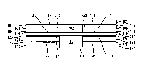
For smaller arrays, an offset or side-by-side configuration is possible, as
shown in
FIGS. 15 and 16. The RF chip 162 is typically much smaller than the antenna
arrays.
11
CA 02713353 2010-07-26
WO 2009/128866 PCT/US2008/088514
Thus, this configuration will not increase the package size much. However, the
feed lines
114 will be longer than the configurations shown in FIGS. 7-14, and thus, the
approach of
FIGS. 15 and 16 is advantageous for small array applications. Offsetting chip
162 in
cavity 160 from antenna cavity 750 prevents undesirable deflection and stress
when chip
162 is mounted in cavity 160, as the layers 102, 106, 108, 109, 110, 112 above
cavity 160
provide support, and thus, no island is needed in cavity 750. The antenna
radiation
patterns are also slightly better in the offset case than the patterns for the
ring cavity case,
since the array is completely filed. However, in at least some instances, the
array feed
lines are more challenging to design in the offset case, especially for larger
arrays.
FIGS. 17-18 show first (receiver) and second (transmitter) sixteen antenna
element phased configurations. In FIGS. 17 and 18, as in the other
illustrative island
embodiments, cavity 750 is defined in layers 106, 108, 109, having island 1702
and outer
portion 1704. For the configurations in FIGS. 17 and 18, the package size is
only 28 mm
x 28 mm, with a 46 mil height (into the page) (note 46 mil = 0.046 inches =
1.17 mm). In
FIG. 17, the RF chip 162 requires coplanar waveguide (CPW) feed antennas so
there are
sixteen microstrip to CPW transitions 1902. Chip 162 resides in chip cavity
160. Note
also feed lines 114, reflectors 144, and ground plane slots 113. The
configuration of FIG.
17 employs one ground plane slot per patch, while that in FIG. 18 employs two
ground
plane slots 113 per patch 104. Note also FIGS. 17 and 18 are top views where
dashed
(hidden) lines are not used, for illustrative convenience - chip 162 in cavity
160 is
located below island 1702, just as in FIGS. 7-14.
One or more embodiments of the invention thus provide a package with a socket
160 for an RF chip 162, and an internal cavity 750 for planar antenna arrays.
The
antenna cavity 750 can be, for example, a circular or rectangular ring, or a
large cavity
for side-by-side configurations (an example of the latter is shown in FIGS. 15
and 16).
Embodiments of the package can implement a planar phased array, preferably
without the
need for vias for RF feed, and in one or more embodiments, with a
substantially equal,
and relatively short, feed line length. If a relative larger phased array is
required, more
antenna elements can be used by enlarging the cavity size, as shown in FIGS. 9-
12.
In view of the description of FIGS. 7-18, it will be appreciated that, in
general
terms, a radio-frequency integrated circuit chip package with N integrated
aperture-
12
CA 02713353 2010-07-26
WO 2009/128866 PCT/US2008/088514
coupled patch antennas, N being at least two, includes N generally planar
patches 104, as
well as at least one generally planar ground plane 110 spaced inwardly from
the N
generally planar patches and substantially parallel thereto. The ground plane
is formed
with N coupling aperture slots 113 therein, and the slots are substantially
opposed to the
patches 104 (in some instances, such as FIG. 18, there may be more than N
slots - for
example, 2N slots, two slots for each patch). N feed lines 114 are spaced
inwardly from
the ground plane 110 and substantially parallel thereto. At least one radio
frequency chip
162 is spaced inwardly from the feed lines 114 and coupled to the feed lines
114 and the
ground plane 110. Note that vias, pads, and anti-pads as described with
respect to FIGS.
1-6 can also be used in the embodiments of FIGS, 7-18. The N patches 104 can
be
arranged to form a planar phased array.
A first substrate layer, such as that formed by bound film 126 and substrate
128,
is spaced inwardly from the feed lines 114, and is formed with a chip-
receiving cavity
160, with the chip 162 being located in the chip-receiving cavity. A second
substrate
layer, such as that formed by films 106, 109 and substrate 108, is interposed
in a region
between the ground plane 110 and a plane defined by the patches 104. The
patches 104
are formed in a first metal layer, the ground plane 110 is formed in a second
metal layer,
and the second substrate layer defines an antenna cavity 750, with the N
generally planar
patches 104 being located in the antenna cavity 750.
In some instances, an island 702, 1702 is formed in the second substrate
layer,
within the cavity 750, thus defining a ring shape of the cavity, and the N
generally planar
patches 104 are located in the ring shape, with the island 702, 1702 being
substantially
opposed to the chip-receiving cavity 160. "Substantially opposed," as used
herein, is
intended to describe a configuration where the island at least partially
overlaps the chip-
receiving cavity when viewed in plan, to help support insertion loads from
insertion of
chip 162 into cavity 160. The island and the cavity may have a variety of
shapes, and
may have the same or different shapes in any particular instance. In some
exemplary,
non-limiting cases, both are substantially rectangular (rectangular
encompassing, but not
limited to, square) when viewed in plan, while in other, exemplary, non-
limiting cases,
both are substantially circular when viewed in plan.
13
CA 02713353 2010-07-26
WO 2009/128866 PCT/US2008/088514
In some instances, a third substrate layer, such as that formed by substrate
112, is
interposed in a region between the ground plane 110 and the feed lines 114,
and the feed
lines 114 are formed in a third metal layer. In one or more embodiments, N
reflectors
144 are spaced inwardly from the third substrate layer and generally opposed
to the
coupling aperture slots 113. The reflectors 144 can be located, for example,
on an inner
surface of the first substrate layer. Furthermore, in some instances, a fourth
substrate
layer, such as that formed by bound film 170 and substrate 172, is spaced
inwardly from
the reflectors 144, with the reflectors 144 being embedded between the first
and fourth
substrate layers.
In other instances, such as shown in FIGS. 15 and 16, the antenna cavity 750
is
spaced away from the chip-receiving cavity 160 when viewed in plan, such that
loads
incurred during insertion of the chip 162 into the chip-receiving cavity 160
are
substantially supported away from the antenna cavity (for example, by
compression in
the layers 102, 108, 106, 109, 110, 112 immediately over chip 162).
In some instances, a cover, such as layer 102, is secured over the antenna
cavity
750, and is at least partially supported by the island 702.
In another aspect, a method of fabricating a radio-frequency integrated
circuit
chip package of the kind described includes providing a package of the kind
described,
without the chip 162 inserted, and with the island 702 as described, as well
as inserting at
least one radio frequency chip 162 into the cavity 160, with the island 702
supporting
loads induced by the insertion of the chip into the cavity.
In yet another aspect, a method of fabricating a radio-frequency integrated
circuit
chip package of the kind described includes providing a package of the kind
described,
without the chip 162 inserted, and with the antenna cavity spaced away from
the chip-
receiving cavity when viewed in plan (as shown, for example, in FIGS. 15 and
16), as
well as inserting at least one radio frequency chip 162 into the cavity 160,
such that loads
incurred during insertion of the chip 162 into the chip-receiving cavity 160
are
substantially supported away from the antenna cavity (for example, by
compression in
the layers 102, 108, 106, 109, 110, 112 immediately over chip 162).
It will be appreciated and should be understood that the exemplary embodiments
of the invention described above can be implemented in a number of different
fashions.
14
CA 02713353 2010-07-26
WO 2009/128866 PCT/US2008/088514
Given the teachings of the invention provided herein, one of ordinary skill in
the related
art will be able to contemplate other implementations of the invention.
Although illustrative embodiments of the present invention have been described
herein with reference to the accompanying drawings, it is to be understood
that the
invention is not limited to those precise embodiments, and that various other
changes and
modifications may be made by one skilled in the art without departing from the
scope of
spirit of the invention.