Note : Les descriptions sont présentées dans la langue officielle dans laquelle elles ont été soumises.
CA 02713473 2010-08-18
DEVICE AND METHOD FOR PROVIDING POWER TO A MICROCONTOLLER
FIELD OF THE INVENTION
[0001] The present invention relates generally to devices for and methods of
providing power to a microcontroller, and more particularly to devices for and
methods of providing power to a microcontroller using a low voltage power
source.
BACKGROUND OF THE INVENTION
[0002] Microcontrollers, or microcontroller units (MCUs), are integrated
circuits that
are generally embedded in devices or products to control aspects of the device
or
product or monitor external events according to the software (firmware)
running on
the MCU. There is generally a desire to minimize the size of such devices,
which has
led to the miniaturization of MCUs.
[0003] However, an MCU requires a power source. This is typically provided by
electrochemical cells, which may be galvanic cell batteries, such as alkaline,
silver
oxide, zinc-carbon and nickel cadmium cells. Each cell generally provides a
maximum of about 1.2 to 1.5 volts. MCUs typically require up to 5 volts, which
is
generally provided by multiple cells. The desire to reduce size has led to the
availability of ultra low power MCU families that utilize CMOS semiconductor
technology. However, even these MCUs require at least 1.8 volts currently, and
so
require at least two cells connected in series, in the absence of voltage
boosting
circuitry. Also, it may be advantageous to use MCUs that require higher
voltages for
cost or other reasons.
[0004] One approach to allowing an MCU to operate with a single cell that has
sufficient energy to power the MCU is to employ a voltage boosting circuit,
also
referred to as a DC-to-DC converter or a step-up voltage converter. Such
converters
generally fall into one of two categories: (1) those that switch the current
flow through
an inductor, and (2) those which that switch the current flow through a
capacitor. The
1
CA 02713473 2010-08-18
latter is often referred to as a "charge pump". Many variants of these types
of
converters are known.
[0005] The use of a separate step-up voltage converter at least partially
defeats the
purpose of using the converter by increasing the size of the device as well as
its cost
and complexity.
[0006] Approaches have been disclosed where some elements of an inductor-based
step-up converter are incorporated into an MCU chip. However they require an
external inductor to operate, which increases the size of the device
significantly. Such
a solution also precludes ultra low power operation due to the current
consumption of
the boost circuit.
SUMMARY OF THE INVENTION
[0007] The invention provides a charge pump device for connecting a direct
current
power source to a microcontroller, which microcontroller operates with an
input
voltage level of at least VCCmin, where VCCmin is greater than the voltage
across
the power source, the charge pump comprising:
a. a supply capacitor connected to the power supply terminal of the
microcontroller;
b. a flying capacitor circuit having a flying capacitor, the flying capacitor
circuit being switchably connected to the power supply terminal of the
microcontroller and to the power source; and
c. firmware for execution by the microcontroller to control the flying
capacitor circuit to repeatedly switch the flying capacitor between being
connected in series with the power source and being connected in
parallel with the power source to top up the charge on the supply
capacitor so that the voltage supplied to the microcontroller is
maintained at a level of at least VCCmin,
2
CA 02713473 2010-08-18
wherein the power source is connected either to the power supply terminal of
the microcontroller or a ground.
[0008] The invention also provides a method of operating a microcontroller,
which
operates with an input voltage level of at least VCCmin, using a direct
current power
source, the power source having an output voltage of less than VCCmin, the
method
comprising the steps of:
a. connecting a flying capacitor circuit having a flying capacitor to the
microcontroller and the power source;
b. programming the microcontroller with firmware to repeatedly switch the
flying capacitor between being connected in series with the power
source and being connected in parallel with the power source;
c. connecting a supply capacitor to the power supply terminal of the
microcontroller to supply a voltage to the microcontroller; and
d. charging the supply capacitor using an external power source so that
the voltage supplied to the microcontroller is at least VCCmin and the
microcontroller begins to execute the firmware,
wherein the switching of the flying capacitor is controlled by the firmware so
as
to maintain the voltage supplied to the microcontroller at a level of at least
VCCmin.
[0009] The switching of the flying capacitor may be performed in a pattern
that is
pre-determined to be sufficient to maintain the voltage supplied to the
microcontroller
at a level of at least VCCmin. The pre-determined switching pattern may be
selected
to maintain the voltage supplied to the microcontroller at a voltage in a pre-
defined
sub-range between a lower level that is greater than VCCmin and an upper level
that
is less than two times the voltage across the power source.
[0010] The supply capacitor may be initially charged by an external power
source to
supply a voltage of at least VCCmin to the microprocessor.
3
CA 02713473 2010-08-18
[0011 ] The microcontroller may monitor the voltage being provided to the
microcontroller and switch the voltage through the flying capacitor as
required to
maintain the voltage being supplied to the microcontroller at a level of at
least
VCCmin.
[0012] The flying capacitor circuit may include two transistors, one being a
high-side
switching transistor and the other being a low-side switching transistor. The
transistors may be either P-channel or N-channel transistors or a mixture
thereof.
The high-side switching transistor may be an N-channel transistor or a P-
channel
transistor. The low-side switching transistor may be an N-channel transistor a
P-
channel transistor. The two transistors of the flying capacitor circuit may be
integrated
on a chip with the microcontroller.
[0013] The power source may comprise at least one galvanic cell and may employ
only a single galvanic cell. The voltage across the power source may be less
than 1.6
volts. VCCmin may be at least 1.8 volts or may be at least 3.0 volts.
BRIEF DESCRIPTION OF THE DRAWINGS
[0014] The present invention will now be described by way of example with
reference to the following drawings.
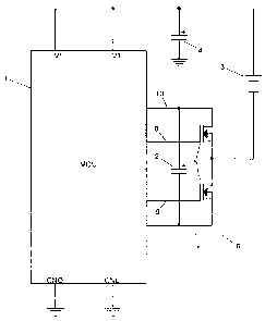
[0015] Figure 1 is a schematic diagram of an embodiment of the invention.
[0016] Figure 2 is a schematic diagram of an embodiment of the invention
showing
internal components of the microcontroller.
[0017] Figure 3 is a schematic diagram of an embodiment of the invention
showing
the flying capacitor circuit connected in parallel with the power source.
[0018] Figure 4 is a schematic diagram of an embodiment of the invention
showing
the flying capacitor circuit connected in series with the power source.
[0019] Figure 5 is a schematic diagram of an alternate embodiment of the
invention
showing the flying capacitor circuit connected in parallel with the power
source.
[0020] Figure 6 is a schematic diagram of an alternate embodiment of the
invention
showing the flying capacitor circuit connected in series with the power
source.
4
CA 02713473 2010-08-18
DETAILED DESCRIPTION OF THE INVENTION
[0021] The invention is a charge pump device for providing power to an MCU
using a
low-voltage power source, such as a single galvanic cell, and methods for
providing
such power.
[0022] Figure 1 shows a schematic diagram of the invention with an MCU 1 and
power source 3. The charge pump includes a flying capacitor circuit 6 and a
supply
capacitor 4. The flying capacitor circuit 6 includes a flying capacitor 2 that
may be
connected to the power source 3 either in series or in parallel. The flying
capacitor
circuit 6 is connected to the MCU 1 so that the MCU 1 can control switching of
the
connection of the flying capacitor 2 and the power source 3 between a series
and
parallel connection. In the embodiment shown in Figure 1, the switching is
facilitated
by two P-type or N-type MOSFET transistors 5 along with the CMOS transistors
inherently present in the general-purpose I/O lines of the MCU 1.
[0023] The MCU 1 may be a standard MCU that requires an input direct current
(DC)
voltage at some minimum level, which we refer to as VCCmin. For example VCCmin
may vary between 1.8 and 5 volts for different MCUs. The MCU 1 may have non-
volatile memory for storage of firmware which is executed when the MCU 1 is
powered up and which controls the operation of the MCU 1.
[0024] The supply capacitor 4 is permanently connected to the supply terminals
of
the MCU 1 as shown in Figure 1. In this application, "connected" means
electrically
connected, and not simply a direct mechanical connection. The supply capacitor
4 is
initially charged by an external source to supply a voltage level to the MCU 1
within
the specified operating range of the MCU 1. The external source may be, for
example, an external programming device, such as a JTAG programmer. The JTAG
programmer attaches to the MCU 1 via pins that are dedicated for firmware
programming on the MCU 1. These pins include the same supply terminals of the
MCU 1. The supply capacitor 4 is charged up by the JTAG programmer while it
remains connected to the MCU 1. The voltage level on the supply capacitor 4 is
defined by the output voltage of the JTAG programmer, which is set to be at
least
VCCmin. The voltage provided to the MCU 1 during the firmware upload is thus
5
CA 02713473 2010-08-18
sufficient for the MCU to operate. After the firmware upload has been
completed, the
MCU 1 begins to execute the firmware, maintaining the voltage on the supply
capacitor 4 as described herein, and the programming device can be safely
disconnected from the MCU.
[0025] The supply capacitor may be selected to have a sufficiently high
capacitance
to hold a voltage of at least VCCmin between two active states when the
microcontroller is in an inactive state and not maintaining VCC actively. The
value of
the capacitance C required to maintain the supply voltage above VCCmin depends
on four known factors: 1) the average current consumption of the MCU 1 over
the
period of time under consideration lavg; 2) the leakage current of the
capacitor Beak; 3)
the length of the period (the time At); and 4) the amount of voltage drop AU
that can
be safely afforded (which depends on the starting voltage point VCC1). It is
necessary that VCC1 - AU > VCCmin. The required value of the capacitance C
equals [(lavg + (leak) = At] / AU.
[0026] The flying capacitor circuit 6 may include two transistors 5 external
to the
MCU 1 that are connected to the terminals of the flying capacitor 2 via the
MCU 1
general-purpose I/O lines. The transistors 5 are configured in a way that
allows
switching the effective arrangement of connections between the flying
capacitor 2
and the power source 3. Figure 2 illustrates the connections with the internal
transistors 21 and 22 which are inherently present in the MCU as part of its
general-
purpose I/O lines' electronic structure, and which are employed as part of the
flying
capacitor circuit 6. The transistors can be switched on or off as may be
required to
connect the flying capacitor 2 parallel to the power source 3 as shown in
Figure 3, by
connecting the negative terminal of the flying capacitor 7 through one
external
transistor 31 to the power source 3 and disconnecting it from the ground 33
via
internal MCU transistors 22, and disconnecting the positive terminal of the
flying
capacitor 10 from the power source 3 via the other external transistor 32 and
connecting it to the MCU power supply terminal via internal transistors 21.
The flying
capacitor 2 can be connected in series with the power source 3 as shown in
Figure 4,
by connecting the positive terminal of the flying capacitor 10 to the power
source 3
6
CA 02713473 2010-08-18
through one transistor 32 and disconnecting it from the MCU power supply
terminal
via internal MCU transistors 21, and disconnecting the negative terminal of
the flying
capacitor 7 from the power source 3 through the other transistor 31 and
connecting it
to the ground via internal transistors 22.
[0027] Although the high-side switching transistor that has one of its
conducting
channel contacts (either the drain or the source) connected to VCC (the high
potential point of the circuit) would typically be a P-channel transistor with
its source
connected to VCC, it could alternatively be an N-channel transistor.
Similarly,
although the low-side switching transistor, which has one of its conducting
channel
contacts (either the drain or the source) connected to VSS (the low potential
point of
the circuit), would typically be an N-channel transistor, it could
alternatively be a P-
channel transistor.
[0028] The firmware that is downloaded to the MCU 1 includes code to control
the
flying capacitor circuit 6 to switch the connection between the flying
capacitor 2 and
the power source 3 between series and parallel. Initially the flying capacitor
2 is
uncharged and the connection established by the firmware is in parallel in
order to
charge the flying capacitor 2. During this phase, the supply capacitor 4
provides the
required current to the MCU 1 at a voltage of at least VCCmin. The flying
capacitor
circuit 6 is then switched to a series connection in which the flying
capacitor 2
together with the power source 3 boosts the voltage across the supply
capacitor 2.
During this phase the charge stored i the flying capacitor 2 is partia;ly
transferred to
the supply capacitor 4, topping up its charge and boosting its voltage. As the
charge
in the iyinn capacitor 2 drops and the voltage provided to the MCI 1 1,
referred to as
"VCC", approaches VCCmin, the flying capacitor circuit 6 is switched back to a
parallel configuration to top up the charge of the flying capacitor 2. This
process is
repeated as required to maintain the voltage level, VCC, provided to the MCU 1
at a
level of at least VCCmin.
[0029] The switching frequency may be fixed so that the flying capacitor 2
becomes
charged to approximately the voltage of the power source 3. In that case VCC
will be
about double the voltage of the power source 3. In the simplest mode, the
supply
7
CA 02713473 2010-08-18
capacitor 4 may be periodically topped up above VCCmin by applying an
appropriate
number of switching cycles when the voltage drops close to VCCmin. The
frequency
of topping up the supply capacitor 4 charge may be reduced by topping the
supply
capacitor 4 up periodically so that VCC is about double the voltage of the
power
supply 3. Conversely, if VCC is maintained close to VCCmin, then the topping
up will
need to be done relatively frequently. In general it is most efficient to
reduce the
amount of switching required so as to reduce power loss that is inherent in
the
switching process.
[0030] The frequency of topping up the supply capacitor 4 may be made to be
very
low depending on the power demands of the MCU 1. When the MCU 1 is in sleep
mode, or inactive, the flying capacitor circuit may be disconnected and no
switching
performed while VCC remains above VCCmin. As described above, the time
interval
between the top-ups is a function of the capacitance of the supply capacitor,
the total
of the sleep and leakage current, and the permissible voltage drop. All of
these
values are known so that a safe time interval between top-ups can be pre-
determined
and the operation of the MCU firmware programmed accordingly.
[0031] The firmware may be designed so that only the charge required to top up
the
flying capacitor 2 a certain amount above VCCmin is transferred to the supply
capacitor 4 so that VCC is always maintained close to VCCmin. It may be
sufficient to
pre-determine a fixed switching pattern consisting of an adequate number of
switching cycles per top-up and a topping up frequency instead of dynamically
determining a switching pattern for maintaining the supply voltage at a level
of at
least V(,(-.min. The calculated fix-r1 switching pattern is design d tn ensure
that the
supply capacitor 4 is always maintained at a level of at least VCCmin_
Employing a
predetermined switching pattern can reduce current consumption and switching
losses compared to variable frequency modes of operation.
[0032] Alternatively, the input voltage VCC may be monitored by the MCU's
analog
to digital converter (ADC). Then the switching pattern may be dynamically
adjusted
by the MCU 1 in order to keep VCC close to the minimum level of VCCmin to keep
the supply current consumption of the entire circuit at a minimum. The voltage
level
8
CA 02713473 2010-08-18
measured by the ADC may be used as feedback to the firmware for maintaining
VCC
near the minimum level of VCCmin. Keeping VCC at or slightly above the minimum
level of VCCmin ensures the longest battery life since it results in the
smallest
achievable current consumption possible for ultra-low power systems.
[0033] If desired, VCC may be maintained within a particular sub-range of the
operating range of a low voltage of VCCmin to a high voltage of double the
voltage of
the power source 3 between a lower level that is greater than or equal to
VCCmin
and an upper level of less than or equal to two times the voltage across the
power
source. For example, if VCCmin is 2.0 volts and the voltage across the power
supply
is 1.5 volts, the sub-range may be chosen to be from 2.1 to 2.4 volts, or from
2.2 to
2.6 volts. The I/O levels may thereby be operated within a desired voltage
range.
Such a voltage level range may be achieved by providing feedback to the
firmware
through sampling, or measuring, of the voltage VCC by the ADC. The firmware
then
may control the flying capacitor circuit 6 to generate a voltage within the
desired
range.
[0034] The flying capacitor 2 in the flying capacitor circuit 6 may be
selected to have
capacitance to provide a voltage rating of the difference between VCCmin, or
slightly
higher, and the power source voltage, which allows the use of low cost and
smaller
parts, thus reducing size, weight and cost of the circuit.
[0035] The flying capacitor 2 in the flying capacitor circuit 6 may have a
small
capacitance value suitable for low power operation using a predetermined fixed
or
variable switching pattern. The amount of charge that the capacitor can hold
at any
given voltage is directly proportional to its capacitance. A capacitor of
small
capacitance will hold less charge than one of large capacitance; it will thus
also
transfer a smaller charge during each switching cycle, resulting in a smaller
voltage
increase for the supply capacitor 4. As the capacitance of the flying
capacitor 2
becomes smaller, more switching cycles are required to provide the same
voltage
increase. This can be done, for example, through bursts of more switching
cycles, or
through more frequent bursts of the same number of cycles, or through more
frequent switching at a higher uniform frequency. The flying capacitor's
capacitance
9
CA 02713473 2010-08-18
cannot be arbitrarily small, since at some point switching at the maximum
possible
frequency would be insufficient to keep the supply voltage from dropping. The
benefit
of smaller flying capacitor capacitance value is the resulting smaller size of
the flying
capacitor 2, which may be important in some designs. The penalty for frequent
switching is the increase in the inevitable switching loss resulting in
reduced system
efficiency.
[0036] The flying capacitor 2 in the flying capacitor circuit 6 may have a
large
capacitance rating suitable for ultra-low power operation by maintaining the
VCC
above VCCmin. Larger capacitance of the flying capacitor 2 will allow in a
smaller
total number of switching cycles to replenish the charge on the supply
capacitor 4.
The system efficiency will improve because of smaller switching losses and
thus the
total power consumption of the system will also be smaller. The penalty for
better
switching efficiency is the increased size, and possibly cost, of the flying
capacitor 2.
[0037] The charge current from the power source 3 that charges the flying
capacitor
2 is limited by the on-resistance of the transistors residing in the standard
GPIO pad
modules integrated in the MCU 1. The standard GPIO pins integrated in the MCU
1
may be combined together to reduce the on-resistance of the transistors
residing in
the standard GPIO pad modules integrated in the microcontroller. The
transistors in
the I/O lines, which act as switches, have some resistance (greater than zero
Ohms)
due to the limitations of the fabrication process. The resistance of the
switch limits the
maximum current which can be sourced or sinked through the corresponding line.
An
embedded MCU design may often have some I/O lines which remain unused. Such
unused lines may be utilized to further improve the operation of the charge
pump.
Combining two I/O lines by connecting them in parallel can reduce the
resulting fine
resistance by factor of two, thus doubling the combined available current.
This allows
for faster charge transfer, halving the time which would otherwise be
required.
[0038] In an alternate embodiment, the power source 3 may be connected between
the flying capacitor circuit 6 and the ground 33. Such an embodiment is shown
in
Figures 5 and 6 which show the flying capacitor circuit connected,
respectively, in
parallel and in series with the power source 3.
CA 02713473 2010-08-18
[0039] The external transistors 5 can be switched on or off as required to
connect
the flying capacitor 2 parallel to the power source 3 as shown in Figure 5, by
connecting the positive terminal of the flying capacitor 10 through one
external
transistor 32 to the power source 3 and disconnecting it from the MCU power
supply
terminal via internal MCU transistors 21, and disconnecting the negative
terminal of
the flying capacitor 7 from the power source 3 via the other external
transistor 31 and
connecting it to the ground 33 via internal transistors 22. The flying
capacitor 2 can
be connected in series with the power source 3 as shown in Figure 6, by
connecting
the negative terminal of the flying capacitor 7 to the power source 3 through
one
transistor 31 and disconnecting it from the ground 33 via internal MCU
transistors 22,
and disconnecting the positive terminal of the flying capacitor 10 from the
power
source 3 through the other transistor 32 and connecting it to the MCU power
supply
terminal via internal transistors 21.
[0040] The only external components of the flying capacitor circuit 6, other
than the
flying capacitor 2, which in the example shown in Figure 1 are the two
external
transistors 5, may optionally be integrated on the same chip as the MCU 1.
While
increasing the cost slightly, this would result in the minimum use of space.
MCU
implementations almost always use at least one main supply capacitor parallel
to the
supply terminals whether or not a charge pump is used. Thus if the transistors
5 are
on the chip with the MCU, the only required additional component as compared
to an
unboosted implementation would be the flying capacitor 2.
[0041 ] It will be appreciated that the above description relates to the
described
embodiments by way of example only. Many variations the system and method for
delivering the invention without departing from the spirit of same will be
clear to those
knowledgeable in the field, and such variations are within the scope of the
invention
as described and claimed, whether or not expressly described.
11