Note : Les descriptions sont présentées dans la langue officielle dans laquelle elles ont été soumises.
CA 02714487 2015-11-06
54106-569
METHODS AND APPARATUS FOR CONTROLLING
A NOTIFICATION APPLIANCE CIRCUIT
This application claims the benefit of United States Provisional Patent
Application Serial No. 61/027,130, filed February 8, 2008, and United States
Provisional Patent Application Serial No. 61/027,144, filed February 8, 2008.
Field of the Invention
The present invention relates to circuits in building systems that provide
signals to devices distributed at different areas of a building or facility.
Background
Fire safety systems include, among other things, detection devices and
notification devices. Detection devices include smoke, heat or gas detectors
that
identify a potentially unsafe condition in a building or other facility.
Detection
devices can also include manually operated pull stations. Notification
devices, often
referred to as notification appliances, include horns, strobes, and other
devices that
provide an audible and/or visible notification of an unsafe condition, such as
a "fire
alarm".
In its simplest form, a fire safety system may be a residential "smoke alarm"
that detects the presence of smoke and provides an audible alarm responsive to
the
detection of smoke. Such a smoke alarm device serves as both a detection
device and
1
CA 02714487 2010-08-06
WO 2009/099663
PCT/US2009/000795
a notification appliance.
In commercial, industrial, and multiple-unit residential buildings, fire
safety
systems are more sophisticated. In general, a commercial fire safety system
will
include one or more fire control panels that serve as distributed control
elements.
Each fire control panel may be connected to a plurality of distributed
detection
devices and/or a plurality of distributed notification appliances. The fire
control panel
serves as a focal point for problem-indicating signals that are generated by
the
distributed detection devices, as well as a source of activation (i.e.
notification)
signals for the distributed notification appliances. Most fire safety systems
in larger
buildings include multiple fire control panels connected by a data network.
The fire
control panels employ this network to distribute information regarding alarms
and
maintenance amongst each other. In such a way, notification of a fire or other
emergency may be propagated throughout a large facility.
Moreover, centralized control of multiple fire control panels in large safety
systems can be accomplished by a dedicated or multi-purpose computing device,
such
as a personal computer. Such a centralized computing device, sometimes
referred to
as a control station, is typically configured to communicate with the multiple
fire
control panels via the data network.
Using this general architecture, fire safety systems are scalable to
accommodate a number of design factors, including the building layout, the
needs of
the building management organization, and the needs of the users of the
building. To
achieve scalability and flexibility, fire safety systems may include, in
addition to one
or more control stations, remote access devices, database management systems,
2
CA 02714487 2010-08-06
WO 2009/099663
PCT/US2009/000795
multiple networks of control panels, and literally hundreds of detection and
notification devices. Fire safety systems may further incorporate and/or
interact with
security systems, elevator control systems, sprinlder systems, and heating,
ventilation
and air conditioning ("HVAC") systems.
One of the many sources of costs in fire safety systems is the wiring and
material costs associated with the notification appliances. Building safety
codes
define the specification for notification appliance wiring, voltage and
current. For
example, according to building safety codes, notification appliances are
intended to
operate from a nominal 24 volt signal which provides the power for the
notification
appliance to perform its notification function. For example, an alarm bell, a
strobe
light, or an electronic audible alarm device operates from a nominal 24 volt
supply.
In general, however, notification devices are required to operate at voltages
as low as
16 volts. The delivery of power to the distributed notification appliances
requires a
significant amount of wiring and/or a significant number of distributed power
sources.
In particular, notification appliances are typically connected in parallel in
what
is known as a notification appliance circuit or NAC. Each NAC is connected to
a
power source, such as a 24 volt source, and includes a positive conductor, a
ground
conductor, and multiple notification appliances connected across the two
conductors.
The power source may be disposed in a fire control panel or other panel. The
positive
and ground NAC conductors serve to deliver the operating voltage from the 24
volt
power source, to the distributed notification appliances. Because the positive
and
ground conductors have a finite conductance, i.e. they have impedance, there
is a
practical limit to how long an NAC may extend from the power source before the
3
CA 02714487 2010-08-06
WO 2009/099663
PCT/US2009/000795
voltage available across the NAC conductors falls below the required operating
voltage.
To address the limitations of NACs due to voltage drop, extending the
coverage of notification appliances often requires increasing the number of
power
sources. To this end, special powered appliance circuit extension devices may
be
employed. These powered extension devices are panels that are connected to an
existing fire control panel and emulate a notification appliance or device to
that fire
control panel. Each powered extension device then provides NAC powered signals
to
additional NACs. The power extension device thus forms a form of "repeater"
for the
notification signal voltage. The use of the powered extension devices
effectively
extends the coverage beyond that may be achieved with a single fire control
panel.
The powered extension device is less costly to implement than a fire control
panel.
To date, one of the issues relating to the powered extension devices includes
the reliability of the switching elements used to connect alarm signals to the
NAC.
Switching elements are necessary to controllably connect the 24 volt alarm
notification signal to the NAC. In particular, in the past, when an extension
device
would receive an "alarm notification signal" from its corresponding fire
control panel,
the extension device would connect its own 24 volt power supply to its
extended NAC
using a relay. Relay contacts, however, present undesirable reliability
issues. While
some reliability issues may be partly addressed by using high quality relays,
such
relays significantly increase the cost of implementation.
Accordingly, there exists a need to reduce costs and increase reliability in
notification appliance circuits of fire safety systems, as well as the devices
that
4
CA 02714487 2015-11-06
54106-569
provide power to those notification appliance circuits.
Summary of the Invention
The above described needs, as well as others, are addressed by at least some
embodiments of the invention that employ a semiconductor device instead of
relays to actuate
notification devices in an NAC. In addition, at least some embodiments of the
invention
employ a hot swap controller or similar control scheme to limit in-rush
current that could
damage the semiconductor device.
A first embodiment of the invention is an arrangement for use in a safety
notification system that includes an alarm signal power source, a first
semiconductor device, a
current sensing unit, and a controller unit. The alarm signal power source is
configured to
generate bias power for activating a notification appliance circuit of a
notification system. The
first semiconductor device has a load path coupled between the alarm signal
power source and
the notification appliance circuit. The current sensing unit is operably
coupled to generate a
sensing signal that is dependent on the current in the load path. The
controller circuit is
operably connected to receive the current sensing signal and to control the
first semiconductor
device responsive to a current sensing signal that exceeds an in-rush current
threshold.
In specific embodiments the controller is also used to control the first
semiconductor switch to provide an alarm signal pattern to the NAC.
One advantage of at least one embodiment is that the control circuit allows
for
a MOSFET (or other semiconductor device) as the main controllable
connection/disconnection device between the alarm voltage and the NAC devices.
According to one aspect of the present invention, there is provided an
arrangement for providing an extension from a first notification appliance
circuit to an
extended notification appliance circuit in a safety notification system, said
arrangement
comprising: an alarm signal power source, the alarm signal power source
configured to
generate bias power for activating a notification appliance circuit of a
notification system; at
5
CA 02714487 2015-11-06
54106-569
=
least a first semiconductor device having a load path coupled between the
alarm signal power
source and the notification appliance circuit; a current sensing unit operably
coupled to
generate a current sensing signal that is dependent on the current in the load
path, the current
sensing signal indicative of whether the current through the load path exceeds
an in-rush
current threshold; a current measurement circuit operably coupled to the
current sensing unit
and configured to determine, based on the current sensing signal, whether the
current through
the load path exceeds a steady state current threshold, the steady state
current threshold being
different from the in-rush current threshold; and a controller circuit
operably connected to
receive the current sensing signal and to control the first semiconductor
device responsive to
the current sensing signal.
5a
CA 02714487 2010-08-06
WO 2009/099663
PCT/US2009/000795
The above describe features and advantages, as well as others, will become
more readily apparent to those of ordinary skill in the art by reference to
the following
detailed description and accompanying drawings.
Brief Description of the Drawings
Fig. 1 shows a schematic block diagram of a portion of an exemplary fire
safety system that incorporates an embodiment of the present invention;
Fig. 2 shows a schematic block diagram of a notification extension device that
incorporates an exemplary embodiment of the present invention;
Figs. 3a and 3b shows a schematic diagram of NACs configured for class A
and class B operation, respectively; and
Fig. 4 shows a schematic block diagram of an exemplary embodiment of the
output circuit of the notification extension device of Fig. 2.
Detailed Description
Fig. 1 shows a safety alarm notification system that incorporates an
arrangement according to the invention. The safety alarm notification system
100
includes a fire control panel 102, a plurality of notification appliance loops
104, 106,
a plurality of extended notification appliance loops 108 and 110, a plurality
of
notification appliances 104a, 106a, 108a, 110a, a plurality of detector loops
112, 114,
a plurality of detection devices 112a, 114a, and a notification extension
system 116.
In general, the safety alarm notification system 100 is illustrated in
simplified format
for exposition purposes. Most safety alarm notification systems will include
multiple
6
CA 02714487 2010-08-06
WO 2009/099663
PCT/US2009/000795
interconnected control panels, not shown, but similar to the fire control
panel 102.
Multiple loops and devices would emanate from each fire control panel.
Moreover,
central control stations and other supervisory and monitoring equipment, not
shown,
are typically employed. Such devices are omitted from Fig. 1 for clarity of
exposition.
The fire control panel, or simply "fire panel," 102 is a device that manages,
powers and communicates with the notification appliances 104a, 106a, 108a,
110a
and the detection devices 112a, 114a. Specific operations and capabilities of
the fire
panel 102 will become more readily apparent as the remainder of the system 100
is
described below. In any event, the fire panel 102 is preferably a device that
is
commercially available, such as, for example, the model XLS, MXL, FS250
devices
available from Siemens Building Technologies, Inc. In general the fire panel
102 is
operable to receive indication of a potential hazard via one or more of the
detection
devices 112a, 114a and communicate the existence that indication to a
centralized
control station, not shown, as well as to other fire panels, also not shown.
The fire
panel 102 is further configured to provide a signal (and power) to at least
the
notification appliances 104a, 106a responsive to a command received from the
centralized control station, responsive to a signal received from another fire
panel, or
responsive to the reception of an indication of a potential hazard via one or
more the
detection devices 112a, 114a. The fire panel 102 also has the capability of
detecting
equipment malfunctions on the device loops 112, 114 and the notification
appliance
loops 104, 106.
The notification appliances 104a, 106a are devices that are distributed
7
CA 02714487 2010-08-06
WO 2009/099663
PCT/US2009/000795
throughout a building or facility and are configured to provide a visual
and/or audible
indication of an alarm condition. As is known in the art, notification
appliances
include alarm bells, electronic alarm devices, strobes, loudspeaker and other
similar
devices. The notification appliances 104a, 106a are connected to the fire
panel 102
via the respective notification appliance loops 104, 106. Notification
appliances 104a,
106a are normally in a ready state. In the ready state, no alarm condition is
present,
but the appliance is capable of generating the notification (i.e. the audible
or visual
indication) in the event of receiving appropriate inputs from the fire panel
102 via the
respective notification appliance loop 104, 106.
The notification appliance loops 104, 106 are the powered conductors that
connect the fire panel 102 to the distributed notification appliances 104a,
106a.
Collectively, the notification appliance loops 104, 106 and their respective
notification appliances 104a, 106a form a notification appliance circuit or
NAC.
Notification loops (and their NACs) can be configured in one of two ways,
commonly known as class A and class B operation. Further detail regarding
class A
and class B configurations are discussed further below in connection with
Figs. 3a and
3b.
Referring again to Fig. 1, the detection devices 112a, 114a are devices that
are
distributed throughout a building or facility and are configured to detect a
safety
hazard, such as the presence of smoke, fire, or noxious gasses. Upon detection
of a
safety hazard, the detection devices 112a, 114a communicate information
indicating
the detection to the fire panel 102 via the corresponding detector loop 112.
The
detection devices 112a, 114a may include network capable smoke detection
devices
8
CA 02714487 2010-08-06
WO 2009/099663
PCT/US2009/000795
well known in the art, such the FP11, HFP11, HFP011, available Siemens
Building
Technologies, Inc. Detection devices 112a, 114a may also include manual pull
stations that are triggered by manual action of a building occupant. Such
detection
devices are well known in the art and are included here only for contextual
purposes.
The detection loops 112, 114 provide the electrical communication link between
the
detection devices 112a, 114a and the fire panel 102. Such loops and their
operation
are also well known in the art.
The notification appliances 108a, 110a may suitably be substantially the same
kinds of devices as the notification appliances 104a, 106a. However, the
notification
appliances 108a, 110a are connected to the notification extension system 116,
as will
be discussed below in further detail.
The notification extension system 116 is a device that provides an extension
from a first notification appliance loop to further appliance loops, in order
to extend
the range of coverage via the first appliance loop. For example, as shown in
Fig. 1,
the notification extension system 116 provides an extension from the
notification
appliance loop 106 to further loops 108, 110. As discussed above, there is a
physical
distance limitation on notification appliance loops 104, 106 due to voltage
losses
along the wire of the loops. The notification extension system 116 provides,
among
other things, a voltage boost sufficient to power the further notification
appliance
loops 108, 110.
As discussed further above, the notification extension system 116 in some
manner emulates a notification appliance to the fire panel 102. To this end,
the
notification extension system 116 is configured to receive notification
signals from
9
CA 02714487 2010-08-06
WO 2009/099663
PCT/US2009/000795
the fire panel 102. These notification signals signify that an alarm should be
indicated
in the same manner as the notification appliances 106a. However, instead of
(or in
addition to) providing a visual or audible notification in response to such a
notification signal, the notification extension system 116 is configured to
generate
further notification signals and provide these signals to the notification
appliances
108a, 110a via the further notification loops 108, 110. Thus, the notification
extension system 116 provides greater coverage of the fire panel 102, and the
notification appliance loop 106.
In accordance with at least one embodiment of the present invention, the
notification extension system 116 includes, among other things, at least one
semiconductor device 120 that controllably connects the notification signal to
the
notification appliances 108a, 110a, and a circuit 122 that helps limit in-rush
current to
the semiconductor device 120. In some embodiments, the notification extension
system 116 further includes a test circuit 124 configured to test the
notification
appliance loops 108 and 110 for continuity and short circuits.
Referring again to the first embodiment described herein, operation of the
circuit of Fig. 1 will be briefly discussed. Under normal circumstances, the
notification appliances 104a, 106a, 108a, 110a are in a ready state, but
generate no
audible or visible notification signal. These normal circumstances represent
the
ordinary day-to-day operation of the building in which no fire or other
emergency
exists. The fire safety system 100, or portions thereof, are tested from time
to time to
ensure that the system is in a ready state. Occasionally, a malfunction may
occur in a
notification loop (e.g. 104, 108) or one of the devices (106a, 108a, 112a).
These
CA 02714487 2010-08-06
WO 2009/099663
PCT/US2009/000795
malfunctions may be uncovered by the testing operations. For example, the test
circuit 124 of the notification extension device 116 (or a similar circuit in
the fire
panel 102) may be used to test the notification loops (e.g. 104, 108) for
continuity
without causing actuation of the notification appliances.
An alarm event occurs when an unsafe condition has been detected. For
example, one of the detector devices 112a may detect a smoke condition
indicative of
a smoke/fire event. The detector device 112a would effectuate communication of
the
alarm condition to the fire panel 102. Alternatively, an alarm event may be
detected
by another device connected to another fire control panel, not shown. Such an
alarm
event would be communicated to the fire panel 102 by the other fire control
panel.
Upon indication of an alarm event, the fire control panel 102 provides a
notification signal to each of the notification loops 104, 106. Each of the
notification
devices 104a, 106a receives the notification signal and generates an audible
and/or
visible notification that alerts the occupants of the building of the detected
unsafe
condition. In addition, the notification extension device 116 receives the
notification
signal from the fire panel 102 via the notification loop 106.
The notification extension device 116 then generates another notification
signal for the extension loops 108, 110. To this end, the at least one
semiconductor
device 120 controllably connects a notification signal voltage (e.g. 24 volts)
generated
within the notification extension device 116 to each of the loops 108, 110. It
has been
determined that when the devices loops 108, 110 are first connected, the
appliances
108a and 110a can create an in-rush current that can degrade the semiconductor
switch 120. In this embodiment, the in-rush limiting circuit 122 operates to
reduce
11
CA 02714487 2010-08-06
WO 2009/099663
PCT/US2009/000795
this in-rush current.
Referring generally to the embodiment of Fig. 1 described above, Fig. 2 shows
an exemplary block diagram of a notification extension device 202 that may
suitably
be employed as the notification extension device 116 of Fig. 1.
Referring now to Fig. 2, the notification extension device 202 includes an
input circuit 204, a processing circuit 206, a DC power supply 208, a battery
charger
circuit 210, a battery circuit 212, a boost circuit 214, and an output circuit
216.
Moreover, the output circuit 216 includes first and second in-rush current
management arrangements 240, 242. Each of the in-rush current management
arrangements includes at least a first semiconductor device 244, a first
current sensing
unit 246 and a first controller circuit 248. The output circuit 216 ideally
also includes
a test circuit, not shown in Fig. 2 but shown in the detailed example of the
output
circuit 216 shown in Fig. 4.
The notification extension device 202 also includes NAC inputs 226, 228,
NAC outputs 218, 220, 222 and 224, and a display 230. The NAC inputs 226, 228
connect to conductors of a notification loop and are configured to receive
notification
signals generated by another source via that notification loop. By contrast,
the NAC
outputs 218, 220, 222 and 224 are connected to originate and provide
notification
signals. The NAC outputs 218, 220, 222 and 224 may provide notification
signals to
devices of two NACs in class A configuration, or devices of one NAC in class B
configuration.
In particular, Figs. 3a and 3b show the notification extension device 202
connected in class A and class B configurations, respectively. In particular,
Fig. 3a
12
CA 02714487 2010-08-06
WO 2009/099663
PCT/US2009/000795
shows the notification extension device 202 connected to an NAC 302 configured
for
class A operation, and Fig. 3b shows the notification extension device 202
connected
to an NAC 352 for class B operation.
Referring to Fig. 3a, the NAC includes a feed conductor 306, a return
conductor 308, a plurality of notification appliances 310, and an end-of-line
(EOL)
resistor 312. The feed conductor 306 is a length of conductor (e.g. 14 or 16
gauge
wire) that is connected to the outputs a positive voltage (24-26 VDC) output
terminal
218 of the notification extension device 202, and extends throughout a
building or
portion of a building such that it passes proximate to, and is electrically
connected to,
each of the notification appliance devices 310. The return conductor 308 is a
length
of similar conductor that is connected to a return reference voltage (e.g.
ground)
terminal 220 of the notification extension device 202. The return conductor
308 also
extends through the same portion of the building such that it passes proximate
to, and
is electrically connected to, each of the notification appliance devices 310.
In this
manner, a complete circuit is formed through each of the notification devices
310 by
the notification extension device 202, the feed conductor 306, and the return
conductor 308.
The EOL resistor 312 is coupled between the remote terminal end portions of
the feed conductor 306 and the return conductor 308. One use of the EOL
resistor
312 is to provide a path for testing the continuity of feed conductor 306 and
return
conductor 308. In particular, a voltage can be applied across the feed
conductor 306
and return conductor 308 and the current measured at the source panel 304 for
continuity. The test voltage can be selected such that it does not activate
the
13
CA 02714487 2010-08-06
WO 2009/099663
PCT/US2009/000795
notification appliances 310, nor pass current therethrough. In the embodiments
described herein, the test voltage applied is a negative voltage. For example,
the test
circuit 249 (see Fig. 2) applies -12 volts DC is applied to the feed conductor
306.
Such a voltage does not activate the notification devices 310, and the only
current
path is through the EOL resistor 312. As will be discussed below, the
notification
extension device 202 includes circuitry capable of determining whether the
test
voltage has passed through the EOL resistor 312 without and open or short
circuit on
either of the feed conductor 306 or the return conductor 308.
During normal (i.e. non-test operation), the notification extension device 202
does not provide any signal on the feed conductor 306. If an alarm
notification is to
be provided, the source panel 304 provides a notification signal to the feed
conductor
306. The notification signal is received by each of the notification devices
310. The
voltage in the notification signal causes the notification devices 310 to
provide visual
or audible notification indications. The alarm notification signal may take
the form of
a constant DC voltage, or a sequential signal of 24 volt pulses.
One of the drawbacks of the class A configuration shown in Fig. 3a is that a
single open in the feed conductor 306 or return conductor 308 will disable any
devices
beyond the position of the open. For example, if an open circuit occurs at
position
309, then the two most remote notification appliances 310 will not have be
activated.
As a consequence, many facilities employ the class B configuration, which
allows for
full operation even in the event of an opening in one of the conductors.
Fig. 3b shows the notification extension device 202 connected to an NAC 352
in the class B configuration. The NAC 352 includes a feed conductor 356, a
return
14
CA 02714487 2010-08-06
WO 2009/099663
PCT/US2009/000795
conductor 358, and a plurality of notification appliances 360. The feed
conductor 356
is a length of conductor (e.g. 14 or 16 gauge wire) that is connected to a
positive
voltage (24-26 VDC) output terminal 218 of the notification extension device
202,
and extends throughout a building or portion of a building such that it passes
proximate to, and is electrically connected to, each of the notification
appliance
devices 360. The feed conductor 356, however, unlike the feed conductor 306 of
Fig.
3a, loops back to the notification extension device 202 and connects to the
output
terminal 222, which also is connected to the positive voltage.
Similarly, the return conductor 358 is a length of conductor that is connected
to a return reference voltage (e.g. ground) terminal 220 of the notification
extension
device 202. The return conductor 358 also extends through the same portion of
the
building such that it passes proximate to, and is electrically connected to,
each of the
notification appliance devices 360. The return conductor 358 also makes a
complete
loop and terminates at another ground terminal 224 of the notification
extension
device 202.
In this manner, a complete circuit is formed through each of the notification
devices 360 by the notification extension device 202, the feed conductor 356,
and the
return conductor 358. An EOL resistor, not shown, may be employed within the
notification extension device 202 to connect the terminals 220 and 222. The
EOL
resistor within the source panel 354 may also be used for testing the
continuity of the
feed conductor 306 and the return conductor 308.
The normal operation of the NAC 352 is essentially identical to the normal
operation of the NAC 302 of Fig. 3a. The only significant difference is that
the NAC
CA 02714487 2010-08-06
WO 2009/099663
PCT/US2009/000795
352 will continue to fully function even if there is a break in the conductor.
In
particular, the loop backs of the feed conductor 356 and the return conductor
358 act
as redundant connections. For example, if the feed conductor 356 is broken
(i.e. open
circuited) at point 359, all of the notification devices 360 on either side of
the break
point 359 still receive the feed voltage, albeit from different terminals of
the
notification extension device 202. Thus, the class B connection provides the
advantage of being able to tolerate at least one fault temporarily with little
or no
reduction in service.
It can further be appreciated from Fig. 3a that in class A configuration, the
notification extension device 202 can connect to two different NACs.
Specifically,
the NAC outputs 218, 220 connect to the loop conductors 306, 308 of the first
NAC
302, and the NAC outputs 222, 224 can be connected to connect to the loop
conductors of a second NAC, not shown.
Referring again to Fig. 2, the input circuit 204 is operably coupled to the
NAC
inputs 226, 228 and is configured to emulate a notification appliance device
connected between the NAC inputs 226 and 228. The input circuit 204 is further
configured to receive an ordinary 18-24 volt notification signal generated
between the
NAC inputs 226, 228. The input circuit 204 is configured to provide an
indication of
the existence of the notification signal to the processing circuit 206. The
details of a
suitable input circuit would be known to those of ordinary skill in the art.
The processing circuit 206 is a processing circuit that is configured to carry
out the logical and supervisory operations of the device 202. To this end, the
processing circuit may include a programmable microprocessor or
microcontroller. In
16
CA 02714487 2010-08-06
WO 2009/099663
PCT/US2009/000795
general, the processing circuit 206 is configured to receive an indication
that a
notification signal has been received at the input circuit 204 and to generate
a
command causing the output circuit 216 to provide a notification signal on the
NAC
outputs 218, 220, 222 and 224. The processing circuit 206 further provides the
signals to enable and disable the DC power supply 208 and the boost circuit
214. The
processing circuit 206 is also configured to control the indicators on the
display 230.
The processing circuit 206 may also suitably be configured to test battery
voltage of
the battery circuit 212, as well as to oversee and evaluate tests of the NACs
connected
to the outputs 218, 220, 222 and 224.
Moreover, the processing circuit 206, as will be discussed below in detail,
cooperates with the elements of the output circuit 216 to carry out various
operations
thereof.
The display 230 may suitably be any device that is capable of communicating
at least rudimentary information regarding the devices and/or NACs associated
with
the device 202. For example, the display 230 may include a plurality of LED
indicators, not shown, which are illuminated to indicate a certain condition,
such as
trouble, a malfunction, circuit power, or other conditions. Suitable display
arrangements would be known to those of ordinary skill in the art.
The DC power supply 208 is a power supply circuit that converts mains AC
electrical power to 26 volts DC for use by the output circuit 216 in
generating
notification signals. The DC power supply 208 also provides lower DC voltage
values at other outputs, not shown, to power the processing circuit 206 and
other
logical elements in the device 202. The DC power supply 208 in some
embodiments
17
CA 02714487 2015-11-06
54106-569
provides power to the battery charger 210. The DC power supply 208 may be a
well-
known configuration of a transformer, diodes and capacitors with little or no
output
voltage regulation.
The battery charger 210 is a circuit that generates a charging voltage that is
provided to the battery circuit 212. Suitable battery charging circuits for
use in fire
safety equipment are well known in the art.
The battery circuit 212 in this embodiment includes two series-connected 12-
volt batteries and generates a nominal voltage of 24 volts DC. As is well
known in
the art, however, the battery voltage will vary, and the battery circuit 212
may
generate 20.4 to 26 volts throughout the useful life of the batteries. The
batteries may
suitably be lead acid batteries.
In this embodiment, the boost circuit 214 is provided to boost the output
voltage of the battery circuit to a slightly higher voltage (i.e. 26 volts) to
allow for the
attached NAC to employ longer conductors. In particular, as discussed in co-
pending
U.S. patent application serial no. 12/148,288, filed April 17, 2008,
employing a higher output voltage for notification
signals helps compensate for I2R losses that occur over the length of the feed
and
return conductors of the NAC. Thus, the boost circuit 214 is a circuit that
receives the
output voltage of the battery circuit 212 and generates a substantially
consistent
output voltage of approximately 26 volts. To this end, the boost circuit 214
may
suitably comprise a switching DC-DC converter in the form of a boost
converter.
Such a circuit would include feedback control of the switch to maintain a
consistent
output voltage. Further detail regarding an exemplary embodiment of the boost
18
CA 02714487 2010-08-06
WO 2009/099663
PCT/US2009/000795
circuit 214 is discussed in U.S. Patent Application serial no. 12/148,288.
The battery circuit 212 and the boost circuit 214 thus cooperate to form a DC
power back-up unit 232 that provides a consistent output voltage throughout
the
useful lifetime of the batteries in the battery circuit 212. The DC power back-
up unit
232 may be implemented in any fire control device that powers a NAC or other
circuit
that is normally powered by two 12-volt batteries.
The output circuit 216 is a circuit that is configured to generate
notification
signals under the command of the processing circuit 206. The power for the
notification signals is derived from the output voltage of either the DC power
supply
208 or the boost circuit 214 to the NAC outputs 218, 220, 222 and 224. The
output
circuit 216 may be configured in class B configuration to provide notification
signals
to a single NAC, or in class A configuration to provide signals to two NACs.
(See
Figs. 3a and 3b)
The in-rush management circuits 240, 242 operate to provide protection
against in-rush currents that can damage semiconductor switches in the path of
the
notification signals. In general, the in-rush current management circuit 240
provides
protection in the path to the NAC outputs 218, 220, and the in-rush current
management circuit 242 provides protection in the path to the NAC outputs 222,
224.
However, if the output circuit 216 is configured for class B operation, then
only the
first in-rush current management circuit 240 is required.
As discussed above, each of the in-rush current management circuits includes
a first semiconductor device 244, a current sensing unit 246 and a controller
circuit
248. The semiconductor device 244 has a load path coupled between the alarm
signal
19
CA 02714487 2010-08-06
WO 2009/099663
PCT/US2009/000795
power source, for example, the lines 208a and 214a, and NAC outputs 218, 220,
222
and 224. The current sensing unit 246 is operably coupled to generate a
sensing
signal that is dependent on the current in the load path of the semiconductor
device
244. The controller circuit 248 is operably connected to receive the current
sensing
signal and to control the first semiconductor device 244 responsive to a
current
sensing signal that exceeds an in-rush current threshold. In a preferred
embodiment,
the controller circuit 248 includes a hot swap controller.
In general, the in-rush current management arrangement 240 is configured to
handle short, instantaneous current spikes that can occur when notification
appliances
in the connected NACs are initially powered. In particular, when the output
circuit
216 generates a notification signal on the NAC outputs 218, 220, 222 and 224,
the
notification appliances connected to the NAC outputs 218, 220, 222 and 224 can
generate an initial current spike. During this spike, which is detected via
the current
sensing unit 246, controller circuit 248 controls the current flowing through
the
semiconductor device 244 to provide the necessary current limitation to
protect the
internal devices during the brief surge. Further detail regarding the
operation of this
circuit is provided in connection with Fig. 4, below.
In operation, the notification extension device 202 monitors the NAC input
226, 228 for a notification signal indicative of trouble, or any other reason
that the
notification devices should be activated. Upon detection of a notification
signal at the
NAC input 226, 228, the input circuit 204 provides a logical indication signal
to the
processing circuit 206. The processing circuit 206, responsive to receiving
the
indication signal from the input circuit 204, provides a signal the output
circuit 216
CA 02714487 2010-08-06
WO 2009/099663
PCT/US2009/000795
indicating that the output circuit 216 should generate a notification signal
on the NAC
outputs 218, 220, 222 and 224.
The processing circuit 206 further enables the output 208a of the DC power
supply 208 if the mains AC power is available. In such a case, the processing
circuit
206 furthermore disables the output of the boost circuit 214. As a
consequence, only
the DC power supply 208, and not the DC back-up power unit 232, provides the
signal power to the output circuit 216. In the event that the mains AC
electrical
power is not available, the processing circuit 206 disables the output 208a of
the DC
power supply 208 and enables the output 214a of the boost circuit 214. As a
result,
the DC power back-up unit 232 formed by the battery circuit 212 and the boost
circuit
214 provides the power to the output circuit 216.
The output circuit 216 then provides the notification signal to the NAC
outputs
218, 220, 222 and 224 using the power provided by either the DC power back-up
unit
232 or the DC power supply 208. In some cases, the processing circuit 206 and
the
output circuit 216 cooperate to modulate information or strobe trigger signals
on the
notification signal. Such operations are known in the art. As will be
discussed further
below, the output circuit may suitably modulate information or signal patterns
onto
the notification signal power using the first semiconductor device 244, and
may even
employ the controller 248 to effectuate such modulation.
The above described device thus provides notification signals having a voltage
that is relatively consistent, regardless of the exact output voltage of the
battery circuit
212, assuming that the battery circuit 212 is operating within acceptable
ranges. In
this embodiment, the relatively consistent voltage exceeds the nominal rated
24 volts
21
CA 02714487 2010-08-06
WO 2009/099663
PCT/US2009/000795
DC of the battery circuit 212.
It will be appreciated that a notification extension device 202 of Fig. 2, or
alternatively of any power source that provides power to NACs, will typically
be
capable of connecting to more than one or two NACs. In such a case, it is
preferable
that separate boost circuits 214 be implemented on only those NACs that
require the
boost to avoid costs. This will allow the individual boost circuits to employ
smaller
and cheaper components as compared to a single boost circuit that provides
power to
all NACs, whether or not they require the boost. Moreover, additional in-rush
current
management circuits should be employed for each addition pair of NAC outputs.
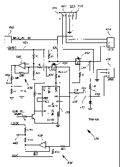
Fig. 4 shows a detailed example of the output circuit 216 of Fig. 2. The
output
circuit includes a first output arrangement 420 and a second output
arrangement 422.
In general, the first output arrangement 420 includes, among other things, an
exemplary embodiment of the first in-rush current management arrangement 240
of
Fig. 2, and the second output arrangement 422 includes, among other things, an
exemplary embodiment of the first in-rush current management arrangement 242
of
Fig. 2. Only the first output arrangement 420 is shown in detail for purpose
of clarity.
The second output arrangement 422 may suitably have a similar structure.
In addition to the first and second output arrangements 420, 422, the output
circuit 216 includes NAC outputs 218, 220, 222 and 224, an EOL resistor 418,
and
configurable terminals 414, 416. The NAC outputs 218, 220, 222 and 224 may
suitably be connected to two NACs when in class A configuration (see Fig. 3a)
or one
NAC when in class B configuration (see Fig. 3b). The switchable terminals 414,
416,
which may suitably take the form of a DIP switch, semiconductor switch, jumper
22
CA 02714487 2010-08-06
WO 2009/099663
PCT/US2009/000795
terminals or other form, are configurable to a first state consistent with
class A
operation and a second state consistent with class B operation. In the first
state, the
switchable terminal 414 connects the NAC output 222 to an output of the second
output arrangement 422, and the switchable terminal 416 connects the NAC
output
224 to ground. In the second state, the switchable terminal 414 connects the
NAC
output 222 to a notification signal output 424 of the first output arrangement
420, and
the switchable terminal 416 connects the NAC output 224 to the EOL resistor
418.
The EOL resistor 418 is serially connected between the notification signal
output 424
and the switchable terminal 416.
Referring now to the first output arrangement 420, the output arrangement 420
includes a current sense resistor 426, semiconductor switches 402, 404, a
controller
circuit 428, a current measurement circuit 430, a test voltage input 432, and
a test
voltage measurement circuit 434. The first output arrangement 420 includes a
notification signal output 424 that is configured for use in class B
configuration only,
and a notification signal output 425 that is configured for use in class A and
class B
configurations.
The current sense resistor 426 is serially connected between a notification
signal voltage source 429 and a current sense node 431. The source 429 may
suitably
be connected to the lines 208a, and/or 214a (see Fig. 2), which provide the 24-
26 volt
output for use as the notification signal. The first semiconductor switch 402,
which
in the form of a MOSFET, is coupled between the current sense node 431 and the
first
notification signal output 425. Similarly, the second semiconductor switch
404,
which is also in the form of a MOSFET, is coupled between the current sense
node
23
CA 02714487 2010-08-06
WO 2009/099663
PCT/US2009/000795
431 and the second notification signal output 424. The first notification
signal output
425 is coupled to the NAC output 218, a terminal OUT of the controller circuit
428,
and an input to the test voltage measurement circuit 434. The second
notification
signal output 424 is coupled to the configurable terminal 414.
The controller circuit 428 includes a current sense input SENSE coupled to the
current sense node 431, and a bias voltage input VCC coupled to the source
429.
With this configuration, the voltage drop between the inputs VCC and SENSE,
divided by the resistance of the current sense resistor 426, provides a
measure of the
current between the source 429 and the NAC outputs 218 and 222. The controller
circuit 428 is configured to detect whether the current through the resistor
426
exceeds a predetermined in-rush current threshold.
To this end, the controller circuit 428 may suitably comprise a hotswap
controller, such as a model TPS2490 or TPS2491 hotswap controller available
from
Texas Instruments, Inc. Other hotswap controllers that have similar inputs and
functions, for example, the MAX4271 controller available from Maxim, are
commercially available and may also be used.
The controller circuit 428 further includes a controlled output GATE that is
operably connected to the gates of the MOSFET switches 402 and 404. The
controller circuit 428 is configured to regulate the gate voltage applied to
the output
GATE in response to the sensed current derived from the input SENSE. The gate
voltage is regulated such that the in-rush current is controllably limited.
In addition, in this embodiment, the controller circuit 428 has an input EN
that
can be used to activate and deactivate the functions of the controller circuit
428, and
24
CA 02714487 2010-08-06
WO 2009/099663
PCT/US2009/000795
in particular, the provision of a signal to the output GATE. The EN input is
operably
coupled to receive a control signal from the processing circuit 206 of Fig. 2.
In
general, the EN input may be used to turn the GATE output on and off to open
and
close, respectively, the MOSFET switches 402, 404. As a result, the control
signal
provided to the EN input may be used to enable and disable the delivery of
notification signals to the NAC outputs 218, 220, 222 and 224 under the
control of the
processing circuit 206. Moreover, the EN input may be used to modulate pulses
onto
the notification signal. For example, if the notification signal is to take
the form of
repeating sequences of three one-second pulses, then the processing circuit
206
provides the control signal to the EN input as a logic signal having the
desired pulse
shape and sequence. The controller circuit 428 then provides corresponding
pulse
signal to the GATE output, thereby causing the switches 402, 404 to be turned
on and
off in accordance with the pulse signal.
As discussed further above, however, one of the main functions of the
controller circuit 428 is to help protect the switches 402, 404 against in-
rush currents.
In addition to protecting against in-rush current, the output circuit 216
assists
in protecting against long term overcurrent conditions. Unlike an in-rush
current,
which is due to temporary large current draws of the notification appliances
as they
are initially activated, a long term overcurrent condition can occur from a
system
issue such as poor (i.e. ohmic) connections in the NAC, low voltage from a
source,
etc. Unlike an in-rush current, which requires temporary limiting until the in-
rush
condition resolves in the normal course, a long term overcurrent condition
indicative
of slow system degradation and can indicate the need for maintenance. If the
CA 02714487 2010-08-06
WO 2009/099663
PCT/US2009/000795
overcurrent is over a limit, it may be necessary to disable the switches 402,
404.
To detect an overcurrent, the current measurement circuit 430 and the
processing circuit 206 of Fig. 2 cooperate to obtain the current sense signal
and
determine whether the current exceeds an overcurrent threshold. The
overcurrent
threshold is different from the in-rush current threshold. This overcurrent
threshold is
set to another value that is indicative of a long term overcurrent problem in
the circuit,
as opposed to an instantaneous spike in current that could be associated with
in-rush.
To carry out such functionality, the measurement circuit 430 includes a
differential
amplifier 438 having differential inputs that are operably coupled to the
source 429
and the current sense node 431. The differential amplifier 438 is configured
via bias
voltages and resistors to provide an output voltage signal at terminal 442
representative of the current through the sense resistor 426. This output
voltage signal
at the terminal 442 is scaled for input to an A/D converter, not shown, which
is part of
the processing circuit 206 of Fig. 2. The processing circuit 206 further
contains logic
to determine if the measured current exceeds the predetermined threshold for a
predetermined time. The predetermined time threshold also ensures that a
measured
overcurrent is not simply an instantaneous spike.
The processing circuit 206 further contains logic to signal the overcurrent
condition in the display 230 or otherwise. The processing circuit 206 also
contains
logic to provide a control signal to disable the switches 402, 404 in the
event of an
overcurrent detection. To this end, the processing circuit 206 is configured
to provide
a suitable control signal to EN input of the controller circuit 428 responsive
to
determining that the measured current exceeds the predetermined threshold for
the
26
CA 02714487 2010-08-06
WO 2009/099663
PCT/US2009/000795
predetermined time. As discussed above, the predetermined threshold and time
are
selected such that ordinary in-rush current events do not trigger the
disabling of the
GATE output.
Thus, while the current sense resistor 426, controller circuit 428, and
MOSFET devices 402, 404 can provide current limiting of in-rush currents,
those
same elements, in combination with the current measurement circuit 430 and
processing circuit 206, further provide protection in the form of a shut-down
in the
event of a steady-state or otherwise less transient overcurrent situation.
As discussed above, the first output arrangement 420 further includes test
voltage circuitry. In particular, the test voltage input 432 and test voltage
measurement circuit 434 cooperate to perform tests that measure for proper
continuity
in the conductors of the NACs attached to the NAC outputs 218, 220, 222 and
224.
The test voltage input 432 is configured to be selectively connected to a
negative
voltage source, and preferably a -12 VDC source. The test voltage input 432 is
further connected to the first notification signal output 425 via a serially
connected
resistor 436. In the embodiment described herein, the resistor 436 is
advantageously
chosen to be the same resistance as the EOL resistor 418, 24 k-ohms.
The test voltage measurement circuit 434 is operably coupled to condition the
voltage on the first notification signal output 425. More specifically, the
test voltage
measurement circuit 434 includes an amplifier 438 having differential inputs
connected to, respectively, the first notification signal output 425 and
biasing voltage
and resistors. The biasing voltages, resistors and the amplifier 438 are
configured to
provide an output voltage that suitable for conversion by an AJD converter not
shown,
27
CA 02714487 2010-08-06
WO 2009/099663
PCT/US2009/000795
in the processing circuit 206. The output voltage at the output terminal 440
of the
measurement circuit 434 is provided to the A/D converter of the processing
circuit
206 of Fig. 2. The processing circuit 206 is configured to determine whether
the
measured voltage is above the first threshold or below the second threshold.
As will
be discussed below in further detail, if the voltage measured by the test
voltage
measurement circuit 434 is above a first threshold, then it is indicative of a
short
circuit in the NAC. If the voltage measured by the test voltage measurement
circuit
434 is below a second threshold, then it is indicative of an open circuit in
the NAC.
The processing circuit 206 is further configured to generate a trouble signal
if
measured voltage is determined to be outside of the acceptable range. The
processing
circuit 206 may further provide, via the display 230, an indication of whether
the
measured test voltage indicates a possible short or a possible open circuit.
In normal operation, the system has three basic conditions, active, inactive
(i.e
ready), or test. In the active condition, an alarm notification signal is
provided to the
NAC outputs 218, 220, 222 and 224. An active condition will occur, for
example,
when a fire or other emergency condition has been detected. In the inactive
condition,
no voltage or notification signal is provided to the NAC outputs 218, 220, 222
and
224. The inactive condition represents the normal, non-emergency condition of
the
fire safety system. In the test condition, also known as "supervisory" mode,
no alarm
notification signal is present, but a special test signal is applied.
In the following description of the operations of the output circuit 216, it
will
be assumed that the NAC outputs 218, 220, 222 and 224 are configured for class
A
operation. Thus, the outputs 218 and 220 are connected to one NAC, and the
outputs
28
CA 02714487 2010-08-06
WO 2009/099663
PCT/US2009/000795
222 and 224 are connected to a different NAC. This arrangement is similar to
that of
Fig. 3a. In such an operation, the switchable terminals 414, 416 are
configured such
that the second output arrangement 422 is coupled to the NAC output 222 and
ground
is connected to the NAC output 224. In general, the operations of the first
output
arrangement 420 are described below. The operations of the first output
arrangement
420 largely do not affect the NAC outputs 222 and 224 in this configuration.
Instead,
the second output arrangement 422 controls the NAC outputs 224, 222. In
general,
however, the second output arrangement 422 operates in the same manner as the
first
output arrangement 420.
In the inactive condition, the NAC output 218 is disconnected from the
notification voltage source 429 by the MOSFET switch 402. To this end, the
processing circuit 206 of Fig. 2 provides a control signal to the controller
circuit 428
that causes the controller circuit 428 to provide little or no gate voltage to
the
MOSFET switches 402. The MOSFET switch 404 also receives no gate voltage.
However, in the class A configuration, the MOSFET switch 404 is disconnected
from
the active part of the circuit of Fig. 4.
In order to place the MOSFET 402 in the off state, the processing circuit 206
provides a disabling control signal to the EN input, thereby causing the
controller
circuit 428 to provide no turn-on voltage to the MOSFET switch 402 via the
output
GATE. Alternatively, or in addition, the actual source 429 of notification
signal
voltage may lack any voltage. In other words, the processing circuit 206 may,
in the
inactive state, cause the source input 429 of the output arrangement 420 to be
disconnected from the 24-26 volt output of the supply 206 and/or boost circuit
214.
29
CA 02714487 2010-08-06
WO 2009/099663
PCT/US2009/000795
(See Fig. 2).
By contrast, in the active condition (i.e. the processing circuit 206
determines
that an alarm condition is present), the processing circuit 206 enables the
controller
circuit 428 by providing a suitable control signal to the EN input of the
controller
circuit 428. In addition, a 24-26 volt signal is received at the source 429.
The first output arrangement 420 controls the application of the 24-26 volt
signal to the NAC connected to the outputs 218 and 220. In particular, the
controller
circuit 428 closes the switch 402. The closing of the switch 402 couples the
24-26
volt notification signal from the source 429 to the NAC output 218, which then
provides the notification signal to the devices of the NAC. The ground
connection to
the NAC output 220 provides ground to the return conductor of the NAC. Upon
initial closing of the switch 402 (and/or providing the 24-26 voltage at the
source
429), the initial current draw of the devices on the NAC can create an in-rush
current.
The controller circuit 428 detects whether this initial current draw or in-
rush current
exceeds a predetermined threshold. To this end, the controller circuit 428
receives a
current sense signal from the current sense node 431. The controller circuit
428
determines the difference between the current sense signal and the voltage at
the input
VCC and divides the resulting difference by the resistance of the current
sense resistor
426 to obtain a current measurement. The controller circuit 428 also compares
the
current measurement to a threshold corresponding to the in-rush current
threshold. If
the current exceeds the in-rush current threshold, then the controller circuit
428
adjusts the gate voltage such that the in-rush current is limited using the
hotswap
controller arrangement, not shown, disposed therein. It is noted that the
controller
CA 02714487 2010-08-06
WO 2009/099663
PCT/US2009/000795
circuit 428 will furthermore shut down the output to the GATE output if the in-
rush
current is not reduced after a predetermined time, for example 15 mSec. The
shutdown delay may be set by attaching a capacitor of a select value
corresponding to
the delay to a TIMER input of the controller circuit 428.
Assuming that the in-rush current expires in a timely manner, the switch 402
will then be in the conductive or "on" state and the 24-26 volts from the
source 429 is
provided to the NAC connected to the outputs 218 and 220. The steady state 24-
26
volts received from the sourced 429 may be directly used as the notification
signal, as
many appliances are designed to provide notification responsive to a simple DC
voltage. However, there are times in which the notification signal has a
pattern, such
as a repeating pattern of pulses. To provide such a pattern, the processing
circuit 206
(of Fig. 2) may provide corresponding pulse signals to the EN input that cause
the
controller circuit 428 to controllably open and close the switch 402 in the
pulsed
pattern.
In the test operation, the processing circuit 206 provides a control signal to
EN
that disables the controller circuit 428. This may occur as a natural result
of being in
the inactive state. The processing circuit 206 (or some other circuit) causes
a -12V
signal to be applied to the test voltage input 432. If the NAC is in good
condition,
then the application of the -12V signal to the test voltage input 432 creates
a -12V
circuit from the test voltage input 432 to the ground connected to the NAC
output
220. The complete circuit includes the resistor 436, the feed conductor (not
shown)
connected to the NAC output 218, the EOL resistor (not shown) of the NAC
connected to the feed conductor, and the return conductor (not shown)
connected to
31
CA 02714487 2010-08-06
WO 2009/099663
PCT/US2009/000795
the NAC output 220. (See also Fig. 3a for an example of a feed conductor 306,
EOL
resistor 312, and return conductor 308 of an NAC 302 connected for class A
operation).
If the NAC is in good working order, then the voltage at the notification
signal
output 425 should be the -12V test voltage divided between the resistor 436
and the
EOL resistor (e.g. EOL resistor 312 of Fig. 3a) of the NAC connected to the
outputs
218, 220. Because the resistor 436 is in this embodiment chosen to be the same
resistance as the EOL resistor, the voltage at the first notification signal
output 425
should be 1/2 of the test voltage, or -6V. By contrast, if the NAC has a short
circuit
between the feed and return conductors, then the EOL resistor of the NAC will
be
bypassed and the entire -12V is dropped over the resistor 436. As a result, a
shorted
NAC will cause the voltage at the output 425 to be near zero. However, if the
NAC
has an open circuit anywhere on the feed and return conductors, then the test
path will
be open circuited, and the entire -12V test voltage will appear at the output
425.
In any event, the test voltage measurement circuit 434 then scales the
measured voltage on the output 425 to a level compatible with the AID
converter of
the processing circuit 206. The processing circuit 206 then compares the
scaled (and
A/D converted) measured voltage value to two thresholds. The first threshold
corresponds to a measured voltage that exceeds -6V by a predetermined amount,
indicating a possible short circuit between the feed and return conductors of
the NAC.
The second threshold corresponds to a measured voltage that is less than -6V
by a
predetermined amount, indicating a possible open circuit (or other source of
high
impedance) in the NAC feed and return conductors. If the processing circuit
206
32
CA 02714487 2010-08-06
WO 2009/099663
PCT/US2009/000795
determines that the measured voltage exceeds the first threshold, then the
processing
circuit 206 indicates an fault condition via the display 230 or other means,
and further
sets an internal fault flag or register value. Similarly, if the processing
circuit 206
determines that the measured voltage is less than the second threshold, then
the
processing device indicates an fault condition via the display 230 or other
means, and
further sets an internal fault flag or register value. If the processing
circuit 206
determines that the measured voltage falls between the two thresholds, then
the
processing circuit 206 may return to normal inactive state operation without
storing a
fault condition flag or indication.
The inactive, active and test operations of the circuit of Fig. 4 will now be
described with reference to a condition in which the NAC outputs 218, 220, 222
and
224 are configured for class B operation. In such a configuration, all of the
outputs
218, 220, 222 and 224 are connected to a single NAC. This arrangement is
similar to
that of Fig. 3b. Thus, in class B configuration, the feed conductor of the NAC
extends
from the NAC output 218, throughout the length of the NAC and back to the NAC
output 222. Similarly, the return conductor extends from the NAC output 220,
throughout the length of the NAC and back to the NAC output 224. In such a
configuration, the switchable terminals 414,416 are configured such that the
NAC
output 222 is connected via the internal EOL resistor 418 to the notification
signal
output 424 and the NAC output 224 is connected directly to the notification
signal
output 424. In class B operation, the first output arrangement 420 controls
all of the
NAC outputs 218, 220, 222 and 224. The second output arrangement 422 is not
used.
33
CA 02714487 2010-08-06
WO 2009/099663
PCT/US2009/000795
In inactive condition, the NAC outputs 218, 220, 222 and 224 are
disconnected from the notification voltage source 429 by the MOSFET switches
402
and 404. To this end, the processing circuit 206 of Fig. 2 provides a control
signal to
the controller circuit 428 that causes the controller circuit 428 to provide
little or no
gate voltage to the MOSFET switches 402, 404.
To turn off the MOSFET switches 402 and 404, the processing circuit 206
provides a disabling control signal to the EN input, thereby causing the
controller
circuit 428 to provide no turn-on voltage at the GATE, which in turn feeds no
voltage
the MOSFET switches 402 and 404. Alternatively, or in addition, the processing
circuit 206 may, in the inactive state, cause the source input 429 of the
output
arrangement 420 to be disconnected from the 24-26 volt output of the supply
206
and/or boost circuit 214.
By contrast, in the active condition (i.e. the processing circuit 206
determines
that an alarm condition is present), the processing circuit 206 enables the
controller
circuit 428 by providing a suitable control signal to the EN input of the
controller
circuit 428. In addition, a 24-26 volt signal is received at the source 429.
The first output arrangement 420 controls the application of the 24-26 volt
signal to the NAC connected to the outputs 218, 220, 222 and 224. In
particular, the
controller circuit 428 closes the switches 402, 404. The closing of the switch
402
couples the 24-26 volt signal from the source 429 to the NAC outputs 222 and
218,
which then provides the signal to the devices of the NAC. The ground
connection to
the NAC output 220 and the NAC output 224 (via Zener diode D2) provides ground
to the return conductor of the NAC. Upon initial closing of the switches 402,
404
34
CA 02714487 2010-08-06
WO 2009/099663
PCT/US2009/000795
(and/or providing the 24-26 voltage at the source 429), the initial current
draw of the
devices on the NAC can create an in-rush current. The controller circuit 428
detects
whether this initial current draw or in-rush current through both switches
402, 404
exceeds a predetermined threshold. As discussed above, the controller circuit
428
derives the current measurement from the current sense signal received from
the
current sense node 431 and the input voltage at the input VCC. As in class A
operation, the controller circuit 428 compares the current measurement to a
threshold
corresponding to the in-rush current threshold. If the current exceeds the in-
rush
current threshold, then the controller circuit 428 adjusts the gate voltage
such that the
in-rush current is limited using the hotswap controller functionality disposed
therein.
As also discussed further above, the controller circuit 428 will furthermore
shutdown
the output to the gate if the in-rush current is not reduced after a
predetermined time,
for example, 15 milliseconds.
Assuming that the in-rush current expires in a timely manner, the switches
402,404 will be in the on-state and the 24-26 volt signal from the source 429
is
provided to the NAC connected to the outputs 222 and 218. As with the class A
operation, the processing circuit 206 (of Fig. 2) may provide pulse signals to
the EN
input that cause the controller circuit 428 to controllably open and close the
switches
402, 404 in the pulsed pattern to create a pulsed notification signal.
In the test operation, the processing circuit 206 provides a control signal to
EN
that disables the controller circuit 428. This may occur as a natural result
of being in
the inactive state. The processing circuit 206 (or some other circuit) causes
a -12V
test voltage to be applied to the test voltage input 432. If the NAC is in
good
CA 02714487 2010-08-06
WO 2009/099663
PCT/US2009/000795
condition, then application of the -12V signal to the test voltage input 432
creates a
complete circuit path for the -12V test voltage between the test voltage input
432 and
the ground connected to the NAC output 220. In the class B configuration, the
complete circuit includes the resistor 436, the feed conductor (not shown)
connected
to the NAC output 218, the looped-back feed conductor (not shown) connected to
the
NAC output 222, the EOL resistor 418, and the return conductor (not shown)
connected to the NAC output 224, and the looped-back return conductor (not
shown)
connected to the NAC output 220. (See also Fig. 3a for an example of a looped
back
feed conductor 356, and a looped back return conductor 358 of an NAC 352
connected for class B operation).
If the NAC is in good working order, then the voltage at the notification
signal
output 425 should be the -12V test voltage divided between the resistor 436
and the
EOL resistor 418. Because the resistor 436 is in this embodiment chosen to be
the
same resistance as the EOL resistor 418, the voltage at the first notification
signal
output 425 should be one-half of the test voltage, or -6V. By contrast, if the
NAC has
a short circuit between the feed and return conductors, then the EOL resistor
418 will
be bypassed and all or much of the -12V test voltage is dropped over the
resistor 436.
As a result, a shorted NAC will cause the voltage at the output 425 to be near
zero.
However, if the NAC has an open circuit anywhere on the feed and return
conductors,
then the test path will be open circuited, and the entire -12V test voltage
will appear at
the output 425.
In any event, the test voltage measurement circuit 434 and processing circuit
206 cooperate as discussed further above to determine whether the voltage at
the
36
CA 02714487 2010-08-06
WO 2009/099663
PCT/US2009/000795
output 425 is within an acceptable window between first and second thresholds.
If the processing circuit 206 determines that the measured voltage exceeds the
first threshold, then the processing device indicates an fault condition via
the display
230 or other means, and further sets an internal fault flag or register value.
Similarly,
if the processing circuit 206 determines that the measured voltage is less
than the
second threshold, then the processing device indicates an fault condition via
the
display 230 or other means, and further sets an internal fault flag or
register value. If
the processing circuit 206 determines that the measured voltage falls between
the two
thresholds, then the processing circuit 206 may return to normal inactive
state
operation without storing a fault condition flag or indication.
Thus, embodiments of the present invention provide among other things, a
way of employing switches for notification signals in an NAC that are not
subject to
the problems of electromechanical relays. Such switches, which are in the form
of
semiconductor switches, are furthermore protected from damage that may be
sustained by in-rush currents that have been found to be created with fire
notification
appliances of an NAC are activated. In one embodiment, a hotswap controller
performs current limiting through the semiconductor switch during the in-rush
current
period.
Some embodiments further include the test circuit that is capable of testing
NACs configured for either class A or class B operation for continuity and
short
circuits. This test circuit further eliminates the need for a special relay,
as was known
in the prior art, to reverse the polarity of the NAC circuit to perform tests.
It will be appreciated that the above describe embodiments are merely
37
CA 02714487 2015-11-06
54106-569
exemplary. Those of ordinary skill in the art may readily devise their own
modifications and implementations that incorporate the principles of the
present
invention and fall within the scope thereof. For example, devices other than
notification extensions devices may employ the technology described herein.
38