Note : Les descriptions sont présentées dans la langue officielle dans laquelle elles ont été soumises.
CA 02715279 2010-08-10
WO 2009/102714 PCT/US2009/033671
RADIO FREQUENCY IDENTIFICATION (RFID) TAG
INCLUDING A THREE-DIMENSIONAL LOOP ANTENNA
TECHNICAL FIELD
[0001] The invention relates to radio frequency identification (RFID) systems
for article
management and, more specifically, to RFID tags.
BACKGROUND
[0002] Radio frequency identification (RFID) technology has become widely used
in
virtually every industry, including transportation, manufacturing, waste
management,
postal tracking, airline baggage reconciliation, and highway toll management.
A typical
RFID system includes a plurality of RFID tags, at least one RFID reader (also
referred to
as an "interrogator") or detection system having an antenna for communicating
with the
RFID tags, and a computing device to control the RFID reader. The RFID reader
includes
a transmitter that may provide energy or information to the tags, and a
receiver to receive
identity and other information from the tags. The computing device processes
the
information obtained by the RFID reader.
[0003] In general, the information received from an RFID tag is specific to
the particular
application, but often provides an identification for an article to which the
tag is fixed.
Exemplary articles include manufactured items, books, files, animals or
individuals, or
virtually any other tangible articles. Additional information may also be
provided for the
article. The tag may be used during a manufacturing process, for example, to
indicate a
paint color of an automobile chassis during manufacturing or other useful
information.
[0004] The transmitter of the RFID reader outputs radio frequency (RF) signals
through
the antenna to create an electromagnetic field that enables the tags to return
an RF signal
carrying the information. In some configurations, the transmitter initiates
communication,
and makes use of an amplifier to excite the antenna with a modulated output
signal to
communicate with the RFID tag. In other configurations, the RFID tag receives
a
continuous wave signal from the RFID reader and initiates communication by
responding
immediately with its information.
CA 02715279 2010-08-10
WO 2009/102714 PCT/US2009/033671
[0005] A conventional tag may be an "active" tag that includes an internal
power source,
or a "passive" tag that is energized by the RF field created by the RFID
reader (typically
by inductive coupling). In either case, the tags communicate using a pre-
defined protocol,
allowing the RFID reader to receive information from one or more tags. The
computing
device serves as an information management system by receiving the information
from the
RFID reader and performing some action, such as updating a database. In
addition, the
computing device may serve as a mechanism for programming data into the tags
via the
transmitter.
SUMMARY
[0006] In general, this disclosure describes a three dimensional (3D) loop
antenna that
may reduce adverse effects to the performance of an RFID tag that are
attributable to the
coupling between the RFID tag and an electrically conductive surface on which
the RFID
tag is placed. RFID tags designed in accordance with this disclosure include a
3D loop
antenna coupled to an RFID circuit. As will be described in detail herein, the
3D loop
antenna includes a first conductive portion having a length and width that
substantially
exceed a thickness of the first conductive portion and lie in a first plane.
The first
conductive portion is electrically coupled to a second conductive portion
having a length
and width that substantially exceed a thickness of the second conductive
portion and lie in
a second plane. The first and second planes are substantially parallel to one
another. A
current is excited through the first and second conductive portions in a
current loop that
lies in a third plane that is not substantially parallel to the first and
second planes. The
current excited through the first and second conductive portions may, for
example, be a re-
modulated interrogation signal that is backscattered by the RFID circuit,
e.g., in the case
of a passive RFID tag. In other instances, e.g., in the case of an active RFID
tag, the RFID
circuit may generate the signal that excites the current through the
conductive portions.
[0007] The RFID tag is configured such that when placed on a surface of an
article the
first and second planes are substantially parallel to the surface of the
article. In this
manner, the plane of the current loop through which the current that is
excited is not
substantially parallel to the article surface to which the RFID tag is
attached. For example,
2
CA 02715279 2010-08-10
WO 2009/102714 PCT/US2009/033671
in some embodiments, the plane in which the current loop of the antenna lies
may be
substantially perpendicular to the article surface.
[0008] In some embodiments, the first and second conductive portions of the 3D
loop
antenna may be defined by an antenna material including one or more portions
defining a
continuous loop for a RF current. In other embodiments, the 3D antenna loop
may be
defined by a combination of the antenna material and an electrically
conductive article
surface on which the RFID tag is placed. In the latter embodiment, the
electrically
conductive article surface and the antenna material define a closed loop for a
current flow.
Thus, the conductive article surface acts as part the 3D antenna. The
electrically
conductive surface and the antenna material may form the closed loop via a
direct
electrical connection or via capacitive coupling.
[0009] The 3D loop antenna may further be designed such that a portion of the
antenna
functions as a tuning element to match an impedance of the antenna to an
impedance of
the IC chip to which the antenna is coupled. As an example, the conductive
trace that
forms the 3D loop antenna may include one or more slits that function as a
capacitive
tuning element. As another example, the 3D loop antenna may have overlapping
conductive portions that function as a capacitive tuning element. As a further
example, the
conductive trace that forms the 3D loop antenna may include a region of
interdigitated
conductive fingers to enhance the capacitance for better tuning.
[0010] The RFID tag may be attached to a substantially non-planar surface of
the article
via a mounting member. The mounting member may be flexible to conform to a
curved or
irregularly shaped (substantially non-planar) surface and may be attached to a
lower
portion of the RFID tag, i.e., between the RFID tag and the article surface.
The mounting
member may be ribbed, include a plurality of sections that are spaced apart
from each
other, or otherwise have a structure that promotes flexibility.
[0011] In one embodiment, a radio frequency identification (RFID) tag
comprises a loop
antenna that includes a first conductive portion having a length and width
that
substantially exceed a thickness of the first conductive portion. The length
and width of
the first conductive portion substantially lie in a first plane. At least a
portion of the first
conductive portion forms a tuning element for tuning an impedance of the loop
antenna.
The loop antenna also includes a second conductive portion having a length and
width that
substantially exceed a thickness of the second conductive portion. The length
and width
3
CA 02715279 2010-08-10
WO 2009/102714 PCT/US2009/033671
of the second conductive portion substantially lie in a second plane that is
substantially
parallel to the first plane. The second conductive portion is electrically
coupled to the first
conductive portion. The RFID tag also comprises an RFID circuit electrically
connected
to the loop antenna to excite a current through the loop antenna to flow
through the first
conductive portion and the second conductive portion in a current loop that
lies in a third
plane that is substantially perpendicular to the first plane and the second
plane.
[0012] In another embodiment, a radio frequency identification (RFID) system
comprises
a reader unit, configured to output an interrogating radio frequency (RF)
field, and an
RFID tag. The RFID tag includes a loop antenna that has a first conductive
portion having
a length and width that substantially exceed a thickness of the first
conductive portion.
The length and width of the first conductive portion substantially lie in a
first plane. At
least a portion of the first conductive portion forms a tuning element for
tuning an
impedance of the loop antenna. The loop antenna also includes a second
conductive
portion having a length and width that substantially exceed a thickness of the
second
conductive portion. The length and width of the second conductive portion
substantially
lie in a second plane that is substantially parallel to the first plane. The
second conductive
portion is electrically coupled to the first conductive portion. The RFID tag
also includes
an RFID circuit electrically connected to the loop antenna to excite a current
through the
first conductive portion and the second conductive portion in a current loop
that lies in a
third plane that is substantially perpendicular to the first plane and the
second plane, to
output an RF signal in response to the interrogating RF signal.
[0013] In another embodiment, an article comprises an electrically conductive
surface and
an radio frequency identification (RFID) tag coupled to the electrically
conductive surface
of the article. The RFID tag comprises a loop antenna comprising a first
conductive
portion having a length and width that substantially exceed a thickness of the
first
conductive portion, wherein the length and width of the first conductive
portion
substantially lie in a first plane. At least a portion of the first conductive
portion forms a
tuning element for tuning an impedance of the loop antenna. The loop antenna
also
comprises a second conductive portion having a length and width that
substantially exceed
a thickness of the second conductive portion, wherein the length and width of
the second
conductive portion substantially lie in a second plane that is substantially
parallel to the
first plane. The second conductive portion is electrically coupled to the
first conductive
4
CA 02715279 2010-08-10
WO 2009/102714 PCT/US2009/033671
portion. The RFID tag also includes an RFID circuit electrically connected to
the loop
antenna to excite a current through the loop antenna to flow through the first
conductive
portion and the second conductive portion in a current loop that lies in a
third plane that is
not substantially parallel to the electrically conductive surface of the
article.
[0014] In another embodiment, an assembly comprises an RFID tag, a mounting
member
configured to mount the RFID tag on a substantially non-planar surface. The
mounting
member comprises a substantially flat and flexible base member comprising an
upper
surface and a lower surface opposite the upper surface, and a plurality of
mounting
structures protruding from the lower surface.
[0015] In another embodiment, a method comprises at least partially filling a
cavity with a
curable resin, pressing a shaping tool into the cavity to shape the resin,
removing the
shaping tool after the material has cured thereby defining a plurality of
mounting
structures extending from a base member, removing the base member and
plurality of
mounting structures from the cavity, the base member being substantially flat
and
comprising an upper surface configured to attach to an radio frequency
identification
(RFID) tag and a lower surface, the mounting structures extending from the
lower surface,
and coupling one or more RFID tags to the upper surface of the base member.
[0016] In another embodiment, a radio frequency identification (RFID) tag
comprises a
loop antenna that includes a first conductive portion having a length and
width that
substantially exceed a thickness of the first conductive portion. The length
and width of
the first conductive portion substantially lie in a first plane. The loop
antenna also
includes a second conductive portion having a length and width that
substantially exceed a
thickness of the second conductive portion. The length and width of the second
conductive portion substantially lie in a second plane that is substantially
parallel to the
first plane. The second conductive portion is electrically coupled to the
first conductive
portion. The second conductive portion is also configured to couple to a
conductive
surface of an article to which the RFID tag is attached. The RFID tag also
comprises an
RFID circuit electrically connected to the loop antenna to excite a current
through the loop
antenna to flow through the first conductive portion, the second conductive
portion, and
the conductive surface of the article to which the RFID tag is attached in a
current loop
that lies in a third plane that is substantially perpendicular to the first
plane and the second
plane.
5
CA 02715279 2010-08-10
WO 2009/102714 PCT/US2009/033671
[0017] In another embodiment, a radio frequency identification (RFID) system
comprises
a reader unit, configured to output an interrogating radio frequency (RF)
field, and an
RFID tag. The RFID tag includes a loop antenna that has a first conductive
portion having
a length and width that substantially exceed a thickness of the first
conductive portion.
The length and width of the first conductive portion substantially lie in a
first plane. The
loop antenna also includes a second conductive portion having a length and
width that
substantially exceed a thickness of the second conductive portion. The length
and width
of the second conductive portion substantially lie in a second plane that is
substantially
parallel to the first plane. The second conductive portion is electrically
coupled to the first
conductive portion. The second conductive portion is also configured to couple
to a
conductive surface of an article to which the RFID tag is attached. The RFID
tag also
includes an RFID circuit electrically connected to the loop antenna to excite
a current
through the first conductive portion, the second conductive portion, and the
conductive
surface of the article to which the RFID tag is attached in a current loop
that lies in a third
plane that is substantially perpendicular to the first plane and the second
plane, to output
an RF signal in response to the interrogating RF signal.
[0018] In another embodiment, an article comprises an electrically conductive
surface and
an radio frequency identification (RFID) tag coupled to the electrically
conductive surface
of the article. The RFID tag comprises a loop antenna comprising a first
conductive
portion having a length and width that substantially exceed a thickness of the
first
conductive portion, wherein the length and width of the first conductive
portion
substantially lie in a first plane. The loop antenna also comprises a second
conductive
portion having a length and width that substantially exceed a thickness of the
second
conductive portion, wherein the length and width of the second conductive
portion
substantially lie in a second plane that is substantially parallel to the
first plane. The
second conductive portion is electrically coupled to the first conductive
portion. The
second conductive portion is also configured to couple to a conductive surface
of an article
to which the RFID tag is attached. The RFID tag also includes an RFID circuit
electrically
connected to the loop antenna to excite a current through the loop antenna to
flow through
the first conductive portion, the second conductive portion, and the
conductive surface of
the article to which the RFID tag is attached in a current loop that lies in a
third plane that
is not substantially parallel to the electrically conductive surface of the
article.
6
CA 02715279 2010-08-10
WO 2009/102714 PCT/US2009/033671
[0019] The details of one or more embodiments of the invention are set forth
in the
accompanying drawings and the description below. Other features, objects, and
advantages of the invention will be apparent from the description and
drawings, and from
the claims.
BRIEF DESCRIPTION OF DRAWINGS
[0020] FIG. 1 is a perspective view of an exemplary radio frequency
identification (RFID)
system for locating a plurality of articles.
[0021] FIG. 2A is a schematic perspective view of one embodiment of an RFID
tag in
accordance with the invention, which includes a 3D antenna, a spacer layer, an
IC chip.
[0022] FIG. 2B is a cross-sectional view of the RFID tag of FIG. 2.
[0023] FIG. 3A is a schematic perspective view of another embodiment of an
RFID tag in
accordance with the invention.
[0024] FIG. 3B is a cross-sectional view of the RFID tag of FIG. 3.
[0025] FIGS. 4A and 4B are graphs demonstrating a relationship between an
impedance
response of an antenna of an RFID tag and a length of the RFID tag.
[0026] FIGS. 5A and 5B are graphs demonstrating a relationship between an
impedance
response of an antenna of an RFID tag and a width of the RFID tag.
[0027] FIGS. 6A and 6B are graphs demonstrating a relationship between an
impedance
response of an antenna of an RFID tag and a height of the RFID tag.
[0028] FIGS. 7A and 7B are graphs demonstrating a relationship between an
impedance
response of an antenna of an RFID tag and a feedpoint of the RFID tag.
[0029] FIG. 8 is a schematic diagram of a testing system for testing a read
range of an
RFID tag.
[0030] FIG. 9 is a perspective view of an exemplary mounting member for an
RFID tag
that enables the RFID tag to be attached to a substantially non-planar
surface.
[0031] FIGS. l0A and l0B illustrate an exemplary configuration for a mounting
member.
[0032] FIG. 1 IA is a plan view illustrating another example configuration for
a mounting
member.
[0033] FIG. 1 lB is a plan view illustrating an additional example
configuration for a
mounting member.
7
CA 02715279 2010-08-10
WO 2009/102714 PCT/US2009/033671
[0034] FIG. 12 is a plan view illustrating yet another example configuration
for a
mounting member.
[0035] FIGS. 13A and 13B illustrate an example process for manufacturing RFID
tags
with a mounting member that enables the RFID tags to be attached to a
substantially non-
planar surface.
[0036] FIGS. 14A-14E are conceptual diagrams illustrating another example
process for
manufacturing RFID tags with a mounting member that enables the RFID tags to
be
attached to a substantially non-planar surface.
[0037] FIG 15A is a schematic perspective view of an example RFID tag in
accordance
with this disclosure.
[0038] FIG. 15B is a cross-sectional view of the RFID tag of FIG. 15A.
[0039] FIGS. 16A and 16B are Smith Charts that illustrate example total
impedance of
two antenna designs.
[0040] FIGS. 17A and 17B are graphs demonstrating example resistance and
reactance
curves that parameterize the length of slit (LSLJT) of RFID tag of FIGS. 15A
and 15B.
[0041] FIGS. 18A and 18B are graphs demonstrating example resistance and
reactance
curves that parameterize the slit offset (SOFFSET) of RFID tag of FIGS. 15A
and 15B.
[0042] FIGS. 19A and 19B are graphs demonstrating example resistance and
reactance
curves that parameterize the slit offset SoFFSET) of RFID tag of FIGS. 15A and
15B.
[0043] FIG. 20A is a schematic perspective view of another RFID tag in
accordance with
this disclosure.
[0044] FIG. 20B is a cross-sectional view of the RFID tag of FIG. 20A.
DETAILED DESCRIPTION
[0045] RFID systems have become widely used in virtually every industry to
track articles
and prevent unauthorized removal of articles from a protected area, such as a
library or
retail store. Conventional RFID tags used in such RFID systems may, however,
encounter
a number of adverse effects when attached to an article that has an
electrically conductive
surface. For example, the coupling between the conventional RFID tags and the
electrically conductive surface of the article to which it is attached may
result in a
decreased read range. In other words, the range over which the tag can be read
is
decreased.
8
CA 02715279 2010-08-10
WO 2009/102714 PCT/US2009/033671
[0046] This disclosure describes a three dimensional (3D) loop antenna that
may reduce
adverse effects to the performance of an RFID tag, such as a decreased read
range, that are
attributable to the coupling between the RFID tag and the electrically
conductive surface
on which the RFID tag is placed. That is, unlike conventional RFID tags that
utilize a
dipole antenna or other substantially two-dimensional (2D) or 3D antenna
configurations,
the read range of a 3D loop antenna designed in accordance with this
disclosure may not
be prohibitively limited when the RFID tag is attached to an electrically
conductive
surface.
[0047] RFID tags designed in accordance with this disclosure include a 3D loop
antenna
coupled to an RFID circuit. As will be described in detail herein, the 3D loop
antenna
includes a first conductive portion having a length and width that
substantially exceed a
thickness of the first conductive portion and lie in a first plane. The first
conductive
portion is electrically coupled to a second conductive portion having a length
and width
that substantially exceed a thickness of the second conductive portion and lie
in a second
plane. The first and second planes are substantially parallel to one another.
A current is
excited in the first and second conductive portions in a current loop that
lies in a third
plane that is not substantially parallel to the first and second planes. The
current excited in
the first and second conductive portions may, for example, be a re-modulated
interrogation
signal that is backscattered by the RFID circuit, e.g., in the case of a
passive RFID tag. In
other instances, e.g., in the case of an active RFID tag, the RFID circuit may
generate a
signal that excites a current through the conductive portions.
[0048] The RFID tag is configured such that when placed on a surface of an
article the
first and second planes are substantially parallel to the surface of the
article. In this
manner, the plane of the current loop through which the RFID circuit excites
current is not
substantially parallel to the article surface to which the RFID tag is
attached. For example,
in some embodiments, the plane in which the current loop of the antenna lies
may be
substantially perpendicular to the article surface.
[0049] In some embodiments, the first and second conductive portions of the 3D
loop
antenna may be defined by an antenna material including one or more portions
defining a
continuous loop for a RF current. In other embodiments, the 3D antenna loop
may be
defined by a combination of the antenna material and an electrically
conductive article
surface on which the RFID tag is placed. In the latter embodiment, the
electrically
9
CA 02715279 2010-08-10
WO 2009/102714 PCT/US2009/033671
conductive article surface and the antenna material define a closed loop for a
current flow.
Thus, the conductive article surface acts as part the 3D antenna. The
electrically
conductive surface and the antenna material may form the closed loop via a
direct
electrical connection or via a capacitive coupling.
[0050] A "3D configuration" indicates that the antenna lies in three
dimensions, and
referencing orthogonal x-y-z axes for ease of description, the antenna has an
x-axis
component, a y-axis component, and a z-axis component. For example, the first
and
second conductive portions of the 3D loop antenna may lie in an x-y plane
while the
portion of the antenna that couples the first and second conductive portion
lies in the y-z
plane. More specifically, the length of the first and second conductive
portions may lie
along the x-axis and the width of the first and second conductive portions may
lie along
the y-axis. The portion of the antenna that couples the first and second
portions to one
another may include a length that lies along the z-axis and a width that lies
along the y-
axis. Such an antenna configuration would cause the current loop to lie in the
x-z plane as
described in further detail below. The 3D loop antenna may operate in the
ultra high
frequency (UHF) range, e.g., in a frequency range of approximately 300
megahertz (MHz)
to approximately 3 gigahertz (GHz). However, other operating ranges in the
radio
frequency spectrum may be used.
[0051] A 3D loop antenna configured in accordance with this disclosure may
reduce
adverse effects to the performance of an RFID tag, such as a decreased read
range, that are
attributable to coupling between the RFID tag and an electrically conductive
surface on
which the RFID tag is placed. In other words, a 3D loop antenna configured in
accordance with this disclosure may maintain, or possibly increase, its read
range even
when coupled to an electrically conductive surface while still maintaining
relatively small
interrogation transmit power of an interrogation device. Rather, the RFID tag
that
includes the 3D loop antenna may, for example, exhibit a read range of greater
than
approximately ten feet (approximately 3 meters) even when attached to an
electrically
conductive surface. The term "read range" generally refers to a communicating
operating
distance between a reader and the RFID tag.
[0052] However, it should be understood the invention is not limited to a read
range of
greater than approximately 10 feet. Rather, as will be described in this
disclosure, the 3D
loop antenna may be designed to support any read range, such as a read range
of less than
CA 02715279 2010-08-10
WO 2009/102714 PCT/US2009/033671
approximately one foot (approximately thirty centimeters), approximately one
foot to
approximately ten feet (approximately thirty centimeters to approximately
three meters),
or greater than approximately ten feet (greater than approximately three
meters). Various
design parameters of the 3D loop antenna may be adjusted to achieve a
desirable trade-off
between performance and size. These trade-offs may be governed by the
particular
application for which the 3D loop antenna is designed.
[0053] Additionally, the RFID tag dimensions may be modified without resulting
in a
detuning of the antenna by adjusting a feedpoint of the antenna. The feedpoint
of the
antenna is the location at which an integrated circuit (IC) chip is coupled to
the antenna.
Thus, the RFID tag may be modified by offsetting the IC chip from the center
of the
antenna to either side. Retuning the 3D loop antenna via adjusting the
feedpoint enables
the RFID tag to have a relatively compact RFID tag structure without
performance
degradation. In some embodiments, the RFID tag may have a relatively small
size, e.g.,
approximately a quarter wavelength or less while maintaining a read range of
approximately 10 feet or greater (approximately 3 meters or greater) without
the need for
increased read power.
[0054] The 3D loop antenna may further be designed such that a portion of the
antenna
functions a tuning element to match an impedance of the antenna to an
impedance of the
IC chip to which the antenna is coupled. As an example, the conductive trace
that forms
the 3D loop antenna may include one or more slits that function as capacitive
tuning
elements. As another example, the 3D loop antenna may have overlapping
conductive
portions that function as a capacitive tuning element. As a further example,
the conductive
trace that forms the 3D loop antenna may include a region of interdigitated
conductive
fingers to enhance the capacitance for better tuning. Although the different
tuning element
designs are described independently, the 3D loop antenna may utilize more than
one type
of tuning element, e.g., overlapping conductive portions and a slit.
[0055] A mounting member is also described for attaching an RFID tag, such as
the RFID
tag described in this disclosure, to a substantially non-planar surface. The
mounting
member, however, is not limited to use with RFID tags including 3D loop
antennas
described in the present disclosure. Rather, the mounting member may be used
to attach
any suitable RFID tag to a substantially non-planar surface. The mounting
member may
include features that promote flexibility, such as a plurality of ribbed
structures that run
11
CA 02715279 2010-08-10
WO 2009/102714 PCT/US2009/033671
along or across the RFID tag, a plurality of pillars that are spaced apart
from each other, a
channeled structure, or other structures that promote flexibility for
attaching the mounting
member to a curved or irregularly shaped (substantially non-planar) surface.
[0056] FIG. 1 is a perspective view of an exemplary radio frequency
identification (RFID)
system 10 for locating a plurality of articles 12A-12N (collectively "articles
12"). RFID
system 10 includes RFID tags 14A-14N attached to articles 12A-12N and a
portable RFID
reader 16, which is adapted to interrogate and obtain data from each of RFID
tags 14A-
14N (collectively, "RFID tags 14"). Articles 12 may be, for example, both
electrically
conductive and nonconductive components. RFID tags 14A-14N each include a
length
that is measured along the x-axis, a width that is measured along the y-axis,
and a height
that is measured along the z-axis. The orthogonal x-y-z axes shown in FIG. 1
are
referenced to aid description of the RFID tag of this disclosure, and are not
intended to
limit the scope in any way. A surface of each of RFID tags 14A-14N in the x-y
plane is
adjacent to the respective article 12A-12N and defines a "contact surface
area." In one
embodiment, an x-y plane of each of RFID tags 14 is attached to the respective
article
12A-12N, such as with a pressure sensitive adhesive, tape or foam, or any
other suitable
mode of attachment. In some embodiments, a mounting member may be attached to
each
of RFID tags 14. In such embodiments, RFID tags 14 are attached to respective
articles
12 via the mounting member.
[0057] The placement of RFID tags 14 on the respective articles 12A-12N
enables RFID
reader 16 to associate a description of an article 12A-12N with the respective
RFID tag
14A-14N via radio frequency (RF) signals 18 and 19. For example, the placement
of
RFID tag 14A on article 12A enables a user to utilize handheld RFID reader 16
to
associate a description or other information related to article 12A with RFID
tag 14A via
RF signals 18 and 19. In an alternate embodiment, reader 16 may be
incorporated into an
automated or semi-automated process and a user does not necessarily need to
utilize reader
16. Reader 16 may interrogate RFID tag 14A by generating RF signal 18, which
is
received by an antenna disposed within RFID tag 14A. The signal energy
typically carries
both power and commands to RFID tag 14A. RFID tag 14A receives the RF energy
radiated by reader 16 and, if the field strength of the RF signal 18 exceeds a
read
threshold, RFID tag 14A is energized and backscatters the RF signal 18 from
the receiver
modulated to include information regarding the object to which the tag is
attached. This
12
CA 02715279 2010-08-10
WO 2009/102714 PCT/US2009/033671
backscattered signal is represented in FIG. 1 as RF signal 19. That is, the
antenna enables
RFID tag 14A to collect energy sufficient to power an RFID circuit, e.g., IC
chip, coupled
to the antenna.
[0058] Typically, in response to one or more commands, the RFID circuit
remodulates the
RF signal from reader 16 and backscatters the modulated signal via the antenna
to output
an RF response to be detected by reader 16. The response may consist of an
RFID tag
identifier, which may match an identifier stored within a database of RFID
handheld
reader 16 or an RFID management system (not shown). Alternatively, the
response may
consist of the transmittal of data from RFID tags 14 to reader 16. Reader 16
may interface
with a data communication port of the RFID management system for communication
of
data between the reader 16 and the RFID management system. The user (or an
automated
or semi-automated machine) may utilize RFID reader 16 to locate one or more
articles 12
by pointing RFID reader 16 at the respective RFID tags 14. Alternatively, one
or more
articles 12 may pass in front of RFID reader 16.
[0059] When an RFID tag that includes an antenna of a type well known in the
art is
attached to an electrically conductive surface, the read range of the RFID tag
may be
substantially reduced. An antenna of a type well known in the art may be a 2D
dipole
antenna, another 2D antenna, or other 3D antennas known in the art. When such
an
antenna is energized by an interrogating RF signal, e.g., RF signal 18, the
interrogating
signal induces currents in the conductive surface on which the RFID tag is
placed. The
currents on the conductive surface create an electromagnetic field. This field
at least
partially cancels the fields produced by the antenna. The conductive surface
also may
cause the impedance of the antenna to shift from the original design value.
The shift of
the antenna impedance and reduced overall field radiated by the antenna may be
reduced
such that it does not exceed the read threshold of the RFID tag. In other
words, the read
range of the RFID tag may be reduced such that the RFID tag is rendered
useless, i.e.,
cannot be read by reader 16 from a useful distance. For example, an RFID tag
may be
attached to a conductive surface of an article, where the article is located
or designed such
that reader 16 cannot be positioned closer than approximately ten feet
(approximately 3
meters) to the RFID tag because of physical limitations. In this case, if the
field strength is
reduced such that the read range is less than ten feet (approximately 3
meters), reader 16
may not be able to read the RFID tag.
13
CA 02715279 2010-08-10
WO 2009/102714 PCT/US2009/033671
[0060] In accordance with this disclosure, however, one or more of RFID tags
14 include
a 3D loop antenna that mitigates at least some of the problems discussed above
with
respect to reduced read ranges in the presence of conductive surfaces. As
discussed with
reference to FIGS. 2 and 3 in greater detail, the 3D loop antenna includes a
first
conductive portion having a length and width that substantially exceed a
thickness of the
first conductive portion and lie in a first plane. The first conductive
portion is electrically
coupled to a second conductive portion having a length and width that
substantially exceed
a thickness of the second conductive portion and lie in a second plane. The
first and
second planes are substantially parallel to one another. A current is excited
through the
first and second conductive portions in a current loop that lies in a third
plane that is not
substantially parallel to the first and second planes. In some instances, the
third plane may
be substantially perpendicular to the first and second planes.
[0061] The 3D loop antenna is configured such that when placed on a surface of
an article
the third plane defined by the current loop is not substantially parallel to
the article surface
to which the RFID tag is attached. In some embodiments, the third plane in
which the
current loop of the antenna lies may be substantially perpendicular to the
article surface.
In other words, one may think of the thicknesses of each of the conductive
portions of the
3D loop antenna defining a plane that is substantially perpendicular to the
article surface.
It should be understood, however, that the 3D loop antenna may be oriented in
any manner
relative to the article surface so long as the third plane defined by the
current loop of the
3D loop antenna is not substantially parallel to the article surface.
[0062] In some embodiments, the antenna is defined by a two-dimensional (2D)
piece of
electrically conductive material that is formed to define a 3D loop. The
electrically
conductive material has a length and width that substantially exceeds the
thickness of the
material, and may therefore be viewed as 2D. When formed to define the 3D
loop, the
electrically conductive material may be viewed as having a first conductive
portion with a
length and width lying in a first plane and a second conductive portion having
a length and
width lying in a second plane that is substantially parallel to the first
plane.
[0063] In other embodiments, the 3D loop antenna is defined by a 2D piece of
conductive
material that is formed to define a portion of a loop and a conductive surface
to which the
RFID tag is attached defines the remainder of the loop. The 2D piece of
conductive
material couples to the conductive surface to form the 3D loop. The coupling
may be an
14
CA 02715279 2010-08-10
WO 2009/102714 PCT/US2009/033671
electrical coupling, e.g., a direct physical electrical connection, or an
electromagnetic
coupling. In this manner, at least a portion of the electrically conductive
article surface
forms the 3D loop antenna. In any case, the 3D loop antenna forms a closed
circuit
through which electrical current continuously flows when the 3D antenna is
energized by
an RF signal.
[0064] In this way, unlike dipole or other 2D antennas well known in the art
in which
current flows in a plane that is substantially parallel to the article surface
to which the
antenna is attached, the 3D loop antenna is oriented such that the 3D loop
antenna may not
experience the adverse effects attributable to an electrically conductive
article surface.
The 3D loop antenna, for example, may not experience a substantially
diminished read
range when attached to or positioned in near contact with an electrically
conductive article
surface. Rather, when energized by an interrogating RF signal, the 3D loop
antenna may
induce image currents in the conductive surface that enhance the read range of
the 3D loop
antenna, i.e., create a electromagnetic field that constructively adds to the
field generated
by the 3D loop antenna. That is, when the 3D loop antenna is in direct contact
or near
contact with an electrically conductive article surface, the article surface
may act as a
ground plane that mirrors or images electromagnetic elements near it. Due to
the
orientation of RFID tag 20 relative to the conductive article surface, as
illustrated in FIGS.
2A, 2B, 3A and 3B, the mirrored or imaged current does not cancel the field
radiated by
the 3D loop antenna, but instead, enhances the field radiated by the 3D loop
antenna.
Thus, the electrically conductive article surface mirrors the electrical
current flowing
through the 3D loop antenna resulting in a "virtual antenna" that is
approximately twice
the size of the 3D loop antenna. The "virtual antenna" includes the 3D loop
antenna and
the mirrored or imaged current loop.
[0065] Regardless of whether the 3D antenna is defined by a piece of
conductive material
or by a piece of conductive material and a conductive surface on which the
RFID tag is
placed, the 3D loop antenna does not induce an electromagnetic field in the
conductive
surface that cancels the field created by the current loop, i.e., the 3D loop
antenna. In fact,
the image currents induced in the conductive surface create a field that
enhances the field
created by the current loop formed by the 3D loop antenna. Consequently, RFID
tags 14
may have an increased read range greater than would otherwise be possible with
other 2D
or 3D antennas known in the art, without significantly increasing the transmit
power of the
CA 02715279 2010-08-10
WO 2009/102714 PCT/US2009/033671
interrogator. The read range of RFID tags 14 may, for example, be greater than
approximately ten feet (greater than approximately 3 meters) while the
transmit power of
the interrogator remains relatively constant. It should be understood,
however, that other
read ranges are possible. Other example read ranges include a read range of
less than
approximately one foot (approximately thirty centimeters) and a read range of
approximately one foot to approximately ten feet (approximately thirty
centimeters to
approximately three meters).
[0066] FIG. 2A is a schematic perspective view of an example RFID tag 20 that
includes
3D loop antenna 22, spacer material 24, and IC chip 26. RFID tag 20 is placed
on article
surface 28. Although not shown in FIG. 2A, RFID tag 20 may include an outer
layer that
helps to protect IC chip 26 and antenna 22 from contaminants, such as
environmental
debris. The outer layer may also be rigid to help protect IC chip 26 and 3D
loop antenna
22 from physical damage. The outer layer may be formed of any suitable
material, such as
a rigid material (e.g., glass or ceramic) or a flexible material (e.g.,
polyimide). In other
embodiments, the outer layer may also extend over sides 42 and 46 and, thus,
completely
encase RFID tag 20.
[0067] IC chip 26 is electrically coupled to 3D loop antenna 22 via opposite
ends 48A and
48B of the 2D strip of conductive material that forms antenna 22. For example,
IC chip 26
may be coupled to antenna 22, i.e., ends 48A and 48B, either directly or by
using vias or
crossovers, and may be embedded within RFID tag 20 or mounted as a surface
mounted
device (SMD).
[0068] IC chip 26 may include firmware and/or circuitry to store within RFID
tag 20
unique identification and other desirable information, interpret and process
commands
received from the interrogation hardware, respond to requests for information
by the
interrogator (e.g., reader 16 of FIG. 1), and to resolve conflicts resulting
from multiple
tags responding to interrogation simultaneously. Optionally, IC chip 26 may be
responsive to commands (read/write) for updating the information stored in an
internal
memory as opposed to merely reading the information (read only). Integrated
circuits
suitable for use in IC chip 26 of RFID tag 20 include those available from
Texas
Instruments located in Dallas, Texas (i.e., the Gen 2 IC line of products),
NXP
Semiconductors located in Eindhoven, Netherlands (i.e., the I-CODE line of
products),
and ST Microelectronics located in Geneva, Switzerland, among others. Although
RFID
16
CA 02715279 2010-08-10
WO 2009/102714 PCT/US2009/033671
tag 20 is described as including an IC chip, other RFID circuitry may be used
in addition
to, or instead of, IC chip 26. For example, RFID tag 20 may include a surface
acoustic
wave (SAW), an organic circuit, or other RFID identification element, or a
combination
thereof.
[0069] In the example shown in FIG 2A, 3D loop antenna 22 includes a first
conductive
portion 40 having a length and width that substantially exceed a thickness of
the first
conductive portion. First conductive portion 40 lies in a first plane 45A. In
the example
illustrated in FIG. 2A, first plane 45A lies in the x-y plane. Loop antenna 22
also includes
a second conductive portion 44 having a length and width that substantially
exceed a
thickness of the second conductive portion. Second conductive portion 44 lies
in a second
plane 45B that is substantially parallel to first plane 45A. More
specifically, second plane
45B also lies in substantially in the x-y plane. First conductive portion 40
is electrically
coupled to second conductive portion 44 via conductive portions 42 and 46.
Thus,
conductive portions 40, 42, 44 and 46 are electrically coupled to form a
closed loop. In
some embodiments, conductive portions 40, 42, 44, and 46 are formed from a
single 2D
strip of electrically conductive material wrapped around spacer material 24 to
define a
loop. In other embodiments, conductive portions 40, 42, 44, and 46 may be made
of more
than one 2D strip.
[0070] The example of FIG. 2A illustrates 3D loop antenna 22 as being a
generally
rectangular loop. Conductive portions 40, 42, 44, and 46 define a rectangular
space that is
substantially filled by spacer material 24. Conductive portions 40 and 44 are
substantially
parallel to each other and generally define sides of the substantially
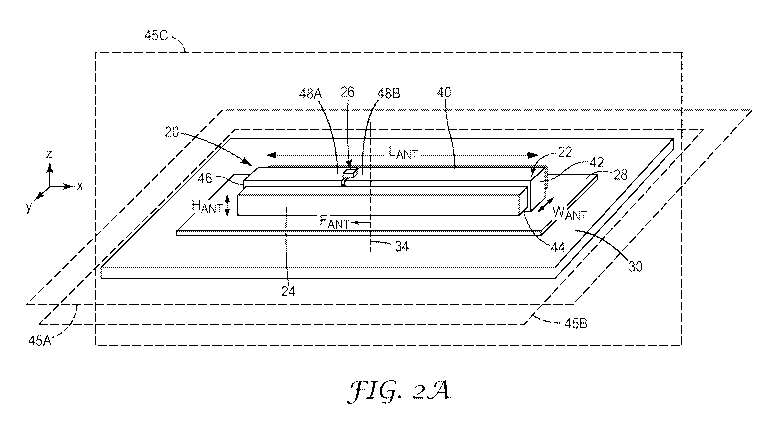
rectangular loop.
Conductive portions 40 and 44 have a length, which is measured along the x-
axis
direction, and a width, which is measured in the y-axis direction. In the
example
illustrated in FIG. 2A, conductive portion 44 and conductive portion 40 have
the same
length and width. However, in other embodiments, conductive portion 40 may be
longer
than conductive portion 44, conductive portion 44 may be longer than
conductive portion
40, conductive portion 44 may be wider than conductive portion 40 or
conductive portion
40 may be wider than conductive portion 44.
[0071] Conductive portions 42 and 46, which couple conductive portions 40 and
44,
define sides of the rectangular loop that are substantially perpendicular to
conductive
portions 40 and 44, and thus planes 45A and 45B. Sides 42 and 46 are
substantially
17
CA 02715279 2010-08-10
WO 2009/102714 PCT/US2009/033671
parallel to each other and each have a length generally equal to the height of
RFID tag 20,
which is measured along the z-axis. Conductive portions 42 and 46 also have a
width
measured along the y-axis direction. In some embodiments, the length and width
of
conductive portions 42 and 46 are substantially larger than a thickness of the
respective
conductive portions.
[0072] Although described as a substantially rectangular loop antenna, 3D loop
antenna
22 of RFID tag 20 may be modified such that 3D loop antenna 22 defines a
greater or
fewer number of sides, thus taking on different shapes. For example,
conductive portions
40 and 44 may not be substantially parallel to one another or conductive
portions 42 and
46 may not be substantially parallel to one another or both.
[0073] Regardless of the number of sides, however, 3D loop antenna 22 may
substantially
define a closed loop through which electrical current continuously flows to
form a closed
circuit when energized by an RF signal, e.g., RF signal 18 (FIG. 1). In
particular, IC chip
26 excites a current through conductive portions 40, 42, 44 and 46 in a
current loop that
lies in a third plane 45C. The current loop through conductive portions 40,
42, 44 and 46
is represented in FIG. 2B by solid arrows in conductive portions 40, 42, 44
and 46. As
illustrated, third plane 45C in which the current loop lies is not
substantially parallel to
first plane 45A and second plane 45B. In some embodiments, the third plane 45C
may be
substantially perpendicular to first plane 45A and second plane 45B.
[0074] In the example illustrated in FIG. 2A, RFID tag 20 is configured such
that when
placed on surface 28 of article 30, the first plane 45A and second plane 45B
are
substantially parallel to surface 28 of article 30. In this manner, current
loop that defines
third plane 45C is substantially perpendicular to article surface 28. However,
the planes
45A, 45B and 45C may be oriented in other positions such that third plane 45C,
i.e., the
current loop that defines the third plane 45C, is not substantially parallel
to article surface
28 to which the RFID tag is attached, but still forms an angle with article
surface 28. That
is, 3D loop antenna 22 may be oriented in any configuration such that plane
45C is not
substantially parallel to article surface 28. It may generally be desirable,
however, to
orient 3D loop antenna 22 such that plane 45C is substantially perpendicular
to article
surface 28 because this configuration may achieve the largest read range.
Orienting 3D
loop antenna 22 such that plane 45C is substantially parallel to article
surface 28 may not
18
CA 02715279 2010-08-10
WO 2009/102714 PCT/US2009/033671
be desirable because such a configuration does not cause image currents in
article surface
28 that constructively add to field generated by 3D loop antenna 22.
[0075] Article surface 28 may be a planar or non-planer surface of an article.
In the
example shown in FIG. 2A, article surface 28 is a planar surface. In some
instances,
article surface 28 is an electrically conductive material, such as, but not
limited to, metallic
materials including copper, aluminum, magnetic metals and metal alloys, such
as
Permalloy, graphite composites, and other materials that are electrically
conductive. RFID
tag 20 may be attached to article surface 28 by an adhesive (not shown). The
adhesive
may be formed of any suitable adhesive, which may depend on the particular
application
of RFID tag 20. For example, in some embodiments, the adhesive may be a
pressure
sensitive adhesive or tape. In alternate embodiments, RFID tag 20 may be
attached to
article surface 28 with a mounting member or other suitable mode of
attachment. FIGS. 9-
12 illustrate example mounting members that may be used for attaching RFID tag
20 to a
generally non-planar surface.
[0076] In any case, RFID tag 20 may be attached to article surface 28 such
that 3D loop
antenna 22 electromagnetically interacts with article surface 28. In FIG. 2A,
a conductive
adhesive may be used to attach RFID tag 20 to article surface 28. As a result,
when 3D
loop antenna 22 is energized by an RF signal, electrical currents within
article surface 28
may enhance the field radiated by antenna 22. In particular, the current
excited through
3D loop antenna 22 induces one or more currents on article surface 28 on which
the RFID
tag is placed. For example, the current that flows through conductive portion
44 may
induce a current on article surface 28. The current induced on article surface
28 is
represented in FIG. 2B by the dashed arrows within article surface 28.
[0077] The induced currents on article surface 28 radiate an electromagnetic
field. Unlike
conventional antenna configurations in which the induced current cancels at
least a portion
of the antenna's field, 3D loop antenna 22 is oriented such that the induced
current on
article surface 28 does not cancel portions of the field radiated by 3D loop
antenna 22.
More specifically, the induced current on article surface 28 does not cancel
the field
radiated by 3D loop antenna 22 because the current loop that defines the third
plane is not
substantially parallel to the plane of article surface 28. In fact, in some
instances the field
radiated by 3D loop antenna 22 may actually be enhanced by the field generated
by the
induced current in article surface 28 due to the orientation of 3D loop
antenna 22. For
19
CA 02715279 2010-08-10
WO 2009/102714 PCT/US2009/033671
example, article surface 28 may act as a ground plane that mirrors or images
3D loop
antenna 22. As will be described in more detail with respect to FIG 2B, the
current loop
formed by 3D loop antenna 22 and electrically conductive surface 28 define a
"virtual
antenna" that is approximately twice the actual size of 3D loop antenna 22.
That is, the
magnitude of the field created by antenna 22 is approximately increased.
[0078] As previously described, some 2D and 3D antenna geometries well known
in the
art may exhibit prohibitively limited read ranges when attached to an
electrically
conductive surface. The electrical currents induced in article surface 28 by
3D loop
antenna 22, however, enable RFID tag 20 to have an increased read range
compared to
many other 2D and 3D antenna geometries known in the art. Experimental results
demonstrating the read ranges for RFID tags similar to RFID tag 20 are
presented below in
Table 1.
[0079] The length LANT, width WANT, and height HANT of 3D loop antenna 22 may
be
selected to increase the effect of the enhanced field created by 3D loop
antenna 22. In
other words, length LANT, width WANT, and height HANT affect a read range of
RFID tag
20. Thus, a particular read range of 3D loop antenna 22 may be optimized at a
particular
range of length LANT, width WANT, and height HANT. In some embodiments, such
as
embodiments in which size is not a paramount design parameter, the length LANT
may be
selected to be in a range of approximately one quarter of a wavelength to
approximately
half a wavelength of the operating frequency of tag 20. Using 915 MHz as an
example,
the length LANT may be selected to be in a range of approximately 0.5 inches
to
approximately 6 inches (approximately 1 centimeters to approximately 15
centimeters).
The width WANT may generally be selected proportional to the length and/or
with other
guidelines in mind. Again, using 915 MHz as an example, width WANT may be
selected in
a range of approximately 0.25 inches to approximately 1.5 inches
(approximately 6
millimeters to approximately 40 millimeters). In some embodiments, the length
and width
of the conductive portions that form 3D loop antenna are substantially larger
than a
thicknesses of the conductive portions. In the example illustrated in FIG. 2A,
conductive
portion 40 and 44 have a length equal to antenna length LANT and a width equal
to antenna
width WANT. Example thicknesses of conductive portion 40 and 44, as well as 42
and 46,
may be in a range of approximately 0.00025 inches to approximately 0.04 inches
CA 02715279 2010-08-10
WO 2009/102714 PCT/US2009/033671
(approximately 0.006 mm to lmm) and, more preferably, approximately 0.001
inches to
0.01 inches (approximately 0.025 mm to 0.25 mm).
[0080] Height HANT of 3D loop antenna 22 depends upon many factors, including
the
height of spacer material 24 disposed between conductive portions 40 and 44.
Height
HANT may be selected such that RFID tag 20 does not protrude significantly
from article
surface 28 to which RFID tag 20 is attached. If RFID tag 20 protrudes
significantly from
article surface 28, RFID tag 20 and/or antenna 22 may be vulnerable to damage.
Height
HANT may also be selected such that 3D loop antenna 22 does not interfere
significantly
with components that are in close proximity to RFID tag 20. As an example,
height HANT
may be in a range of approximately 0.02 inches to approximately 0.4 inches
(approximately 0.5 millimeters to approximately 10 millimeters). It should be
understood
that other heights are possible.
[0081] For operating frequencies greater than 915 MHz, the length LANT and
height HANT
may decrease accordingly, and for operating frequencies less than 915 MHz, the
length
LANT and height HANT may increase accordingly. Therefore, it should be
understood that
these values are merely exemplary and should not be taken as limiting the
scope of the
present invention in any way. Further, although it is generally considered
desirable for an
RFID tag to be as small in size as possible, RFID tags described in this
disclosure, such as
RFID tag 20, may be constructed of any size suitable for the application.
[0082] Spacer material 24 may be formed of a solid material or a material
consisting of
mass particulate matter. Suitable spacer materials 24 include relatively light
weight,
electrically nonconductive materials, such as, but not limited to,
polycarbonate. Another
suitable spacer material could be a low loss magnetic material. RFID tag 20
may also be
constructed without spacer material 24. That is, the center or hole of the 3D
loop antenna
22 may be filled with air instead of a solid material. In this manner, air may
act as a
spacer material 24. Air may be desirable and particularly advantageous in
applications
such as aerospace and other transportation applications because of its
relatively light
weight compared to solid or mass particulate materials.
[0083] The specific properties of 3D loop antenna 22 depend on the desired
operating
frequency of the RFID tag 20. Antenna 22 receives radio frequency (RF) energy
radiated
by an interrogator (e.g., reader 16 of FIG. 1). For example, the RF signal
emitted by the
interrogator may be an ultra high frequency (UHF) RF signal, which typically
refers to a
21
CA 02715279 2010-08-10
WO 2009/102714 PCT/US2009/033671
frequency in a range of about 300 megahertz (MHz) to about 3 gigahertz (GHz).
This RF
energy carries both power and commands to RFID tag 20. In one embodiment, 3D
loop
antenna 22 collects RF energy from the interrogator and operates to convert
the energy to
power IC chip 26, which provides the response to be detected by the
interrogator. Thus,
the properties or characteristics, i.e., design parameters, of 3D loop antenna
22 should be
matched to the system in which it is incorporated.
[0084] More specifically, in order to achieve increased power transfer, the
impedance of
3D loop antenna 22 may be conjugately matched to the impedance of IC chip 26.
Generally, silicon RFID IC chips have a low resistance and a large negative
reactance.
Thus, to achieve conjugate matching, 3D loop antenna 22 may be designed to
have an
equivalent resistance and an equal and opposite large positive reactance.
However, when
3D loop antenna 22 is brought in close proximity, i.e., electromagnetic
contact (or
interaction) with an electrically conductive material, such as metals or
liquids, the
impedance of 3D loop antenna 22 is detuned, resulting in a loss of power
transfer. With
respect to 3D loop antenna 22, in particular, the impedance of 3D loop antenna
22 is
changed when it is attached to a conductive surface, such as article surface
28.
[0085] The dimensions of 3D loop antenna 22, i.e., length LANT, width WANT,
and height
HANT, may be adjusted to match the impedance of 3D loop antenna 22 to the
impedance of
IC chip 26. In addition, a feedpoint FANT, which is the location on 3D loop
antenna 22 at
which IC chip 26 is coupled, may also be adjusted to change the impedance of
3D loop
antenna 22 to better match the impedance of IC chip 26. As illustrated in FIG.
2, the
feedpoint FANT is measured between a center 34 of RFID tag 20, represented by
the
vertical dashed line in FIG. 2, and the location of IC chip 26. In some
embodiments, the
feedpoint FANT may be adjusted such that IC chip 26 is directly connected to
article
surface 28. In this case, IC 26 is directly connected to ground. If the
feedpoint FANT was
adjusted in this way in FIG. 2A, IC chip 26 would be illustrated as being
positioned on
side 42 or side 46. The impedance matching of 3D loop antenna 22 to that of IC
chip 26
may be referred to as "tuning" of 3D loop antenna 22.
[0086] FIG. 2B is a cross-sectional view of RFID tag 20 in conjunction with
article
surface 28. Similar reference numbers reference similar features. As described
above, RF
signal 18 excites a current through 3D loop antenna 22, thus generating a
current loop
through conductive portions 40, 42, 44 and 46. The current loop through 3D
loop antenna
22
CA 02715279 2010-08-10
WO 2009/102714 PCT/US2009/033671
22 is illustrated by the arrows. Article surface 28 may act as a ground plane
if article
surface 28 is reasonably large. Using image theory a representative electrical
model of 3D
loop antenna 22 can be created. Using the electrical model, it can be seen
that due to
article surface 28, the area of the current loop is approximately twice as
large as the
physical area of 3D loop antenna 22. In particular, the article surface 28 can
enhance the
area of the current loop which can enhance the overall radiation.
[0087] In another example, at least a portion of the 3D loop antenna is
defined by a
portion of the conductive article surface on which the RFID tag is attached.
This example
is illustrated in further detail in FIGS. 3A and 3B.
[0088] FIG. 3A is a schematic perspective view of another example
configuration for an
RFID tag 50 that includes a 3D loop antenna 52. In FIG. 3A, RFID tag 50
includes 3D
loop antenna 52, a spacer material 54, IC chip 26, and article surface 58. In
general, RFID
tag 50 operates in a similar manner as RFID tag 20 in FIG. 2. However, the
configuration
of RFID tag 50 differs from that of RFID tag 20. In particular, the 2D strip
of electrically
conductive material 60 in FIG. 3A does not wrap completely around spacer
material 54.
Instead, 2D strip 60 includes structures 51A and 5lB on opposite ends of the
2D strip 60
that couple to article surface 58. In this manner, article surface 58 forms at
least a portion
of 3D loop antenna 52.
[0089] In one example, structures 51A and 51B may be directly connected to
article
surface 58, i.e., electrically connected to article surface 58. In another
example, structures
51A and 51B may be indirectly connected to article surface 58, e.g., connected
to article
surface 58 via electromagnetic coupling. That is, structures 51A and 51B may
"directly"
contact article surface 58 in the former example, e.g., via a conductive
adhesive, and
contact surface 58 through electromagnetic coupling in the latter example,
e.g., through a
gap layer. The gap layer may, for example, comprise a non-conductive adhesive
that
forms an electrical "gap" between structures 51A, 51B and article surface 58.
However, in
both cases, at least a portion of 3D loop antenna 52 is formed by article
surface 58 when
RFID tag 50 is energized by an RF signal. More specifically, electrical
current
continuously flows through the 2D strip of conductive material 60 and a
portion of article
surface 58 to form a closed circuit.
[0090] As shown in FIG. 3A, 2D strip 60 may comprise two separate 2D strips
electrically
coupled to IC chip 26. However, in the interest of clarity, the two separate
2D strips may
23
CA 02715279 2010-08-10
WO 2009/102714 PCT/US2009/033671
be collectively referred to as "2D strip 60" in this disclosure. In other
embodiments, 2D
strip of conductive material 60 may comprise a single continuous piece of
conductive
material. FIG. 3A illustrates 2D strip 60 as defining three conductive
portions 62, 64, and
66 and structures 51A and 51B. In this disclosure, structures 51A and 5lB
maybe
referred to as "wings 51A and 51B" or "contact points." Conductive portions
62, 64, and
66 are positioned to wrap around spacer material 24 while leaving the bottom
portion of
spacer material 24 exposed to article surface 58. In this manner, conductive
portions 62,
64, 66 and article surface 58 define a space that is substantially filled by
spacer material 24
and conductive portions 66 and 64 each define planes that are substantially
perpendicular
to at least a portion of the plane of article surface 58. In some embodiments,
article
surface 58 may also include a curvilinear portion, in which case conductive
portions 64
and 66 may not be substantially perpendicular to the entire article surface
58. As
previously described with respect to FIG. 2, spacer material 24 may be air or
a solid
dielectric material, such as, but not limited to, polycarbonate.
[0091] First conductive portion 60 of 3D loop antenna 52 has a length and
width that
substantially exceed a thickness of first conductive portion 60. First
conductive portion 60
lies in a first plane 55A. In the example illustrated in FIG. 2, first plane
55A lies in the x-y
plane. Wings 51A and 51B of 3D loop antenna 52 also have a length and width
that
substantially exceed a thickness of wings 51A or 51B. Wings 5 1A and 51B lie
in a second
plane 55B that is substantially parallel to first plane 55A. More
specifically, second plane
55B also lies substantially in the x-y plane. First conductive portion 62 is
electrically
coupled to wings 51A and 51B via conductive portion 66 and 64, respectively.
[0092] RF signal 18 excites a current through conductive portions 62, 64, and
66 and
article surface 58 in a current loop 57A that lies in a third plane 55C. As
illustrated, third
plane 55C in which the current loop 57A lies is not substantially parallel to
first plane 55A
and second plane 55B. In some embodiments, the third plane 55C may be
substantially
perpendicular to first plane 55A and second plane 55B. In the example
embodiment
illustrated in FIG. 3A, third plane 55C lies in the x-z plane, which is
perpendicular to the
x-y plane.
[0093] In the example illustrated in FIG. 3, RFID tag 50 is configured such
that when
placed on article surface 58, the first plane 55A and second plane 55B are
substantially
parallel to article surface 58. In this manner, current loop 57A that defines
third plane 55C
24
CA 02715279 2010-08-10
WO 2009/102714 PCT/US2009/033671
is substantially perpendicular to article surface 58. However, the conductive
portions may
be oriented in other positions such that current loop 57A defines a third
plane that is not
substantially parallel to article surface 58 to which the RFID tag is
attached, but still forms
an angle with article surface 58. That is, 3D loop antenna 52 may be oriented
in any
configuration such that plane 55C is not substantially parallel to article
surface 58. It may
generally be desirable, however, to orient 3D loop antenna 52 such that plane
55C is
substantially perpendicular to article surface 58 because this configuration
may achieve
the largest read range.
[0094] As shown in FIG. 3A, conductive portion 62 has a length LP1 and is
substantially
parallel to article surface 58. The conductive portions that form wings 51A
and 51B have
lengths LPZa and LPZb, respectively. Lengths LPZa and LPZb may, for example,
be
approximately, 0.5 inches and 1 inch. In the example, lengths LPZa and LPZb
are of
substantially equal lengths. In other embodiments, however, lengths LPZa and
LPZb may be
different lengths. Conductive portions 64 and 66 are substantially parallel to
each other
and have a length generally equal to height HANT. In other embodiments,
conductive
portions 64 and 66 may not be substantially parallel to one another.
Conductive portions
62, 64, and 66 and wings 51A and 51B have uniform width WANT measured along
the y-
axis direction. In other embodiments, however, the widths of any of conductive
portions
62, 64, and 66, or wings 51A and 51B may vary. Wings 51A and 51B extend beyond
spacer material 24 on either side along the x-axis direction, and directly or
electromagnetically couple 2D strip 60 to article surface 58. In this manner,
wings 51A
and 51B act as contact points that couple 2D strip 60 to article surface 58.
When 2D strip
60 and article surface 58 are electromagnetically coupled to each other, each
wing 51A and
51B serves as one side of a parallel plate capacitor with the other side being
formed by the
underlying portions of article surface 58. Wings 51A and 51B maybe sized such
that the
capacitor approximates a short circuit or such that it forms another impedance
tuning
element. As described above with respect to FIG. 3, conductive portions 62, 64
and 66
and/or wings 51A and 51B may have varying widths and lengths.
[0095] The size of wings 51A and 51B, and particularly, the surface area that
contacts
article surface 58, may be selected based on the desired capacitance value.
For example,
Equations 1 and 2 below may be used to calculate the size of wings 51A, 51B
necessary to
achieve a particular capacitance value. The operating frequency may be input
into
CA 02715279 2010-08-10
WO 2009/102714 PCT/US2009/033671
Equation 1 along with a value for the impedance that is sufficient for
achieving a short
circuit. Equation 1 can then be solved for a capacitance value C. The
calculated value for
the capacitance value C can then be input into Equation 2 with the value for
the dielectric
constant and a distance, i.e. distance between one of wings 51A or 5lB and
surface 58.
Equation 2 can then be solved for the area which can be used to design the
size of wings
51 A and 51B. Using an operating frequency of 915, for example, a capacitance
of
approximately 30 pico Farads (pF) or more may be desirable to approximate a
short
circuit.
Equation 1 (Z = 1/jwC) Z= I
J
Equation 2 (C=EA/D) C = D
In the equations above, Z is a reactance, co is a frequency in radians per
second, C is a
capacitance, A is an area of a capacitive plate, D is a distance between
capacitive plates
and r, is a dielectric constant of a gap.
[0096] Generally, RFID tag 50 operates in a manner similar to RFID tag 20.
That is, when
energized by an RF signal, electric current continuously flows through 3D loop
antenna
52, e.g., 2D strip 60 and a portion of article surface 58 between wings 51A
and 51B.
However, not only does article surface 58 act as a portion of the 3D loop
antenna, a current
is induced in article surface 58. For example, article surface 58 again may
act as a ground
plane that mirrors or images the current in 2D strip 60. As will be described
in more detail
with respect to FIG. 3B,, the current loop relative to article surface 58
results in a mirrored
current enhancing the field radiated by 3D loop antenna 52. In this way, 3D
loop antenna
52 operates as if it was approximately twice the size of 3D loop antenna 52.
In other
words, the magnitude of the resulting field is increased, thereby increasing
the read range
of 3D loop antenna 52.
[0097] Again, a particular length LANT, width WANT, and HANT may be selected
to tune 3D
loop antenna 52. In addition, the length and width of conductive portions 62
(Lp1), 64, and
66 and wings 51A and 51B (LP2a and LP2b) may be selected to tune 3D loop
antenna 52.
Spacer material 54 in RFID tag 50 may be the same as spacer material 24 used
for RFID
tag 20. Additionally, feedpoint FANT may be adjusted to achieve the same read
range but
26
CA 02715279 2010-08-10
WO 2009/102714 PCT/US2009/033671
with a reduced length LANT and/or thickness HANT of the RFID tag 50. This is
described in
further detail below.
[0098] RFID tag 50 may be attached to article surface 58 in a manner similar
to RFID tag
20. That is, an adhesive, such as a pressure sensitive adhesive, tape, or
foam, may be
attached to the lower portion of RFID tag 50 in order to secure it to surface
58. In some
embodiments, the adhesive may applied to spacer material 54 and wings 51A and
51B. In
other embodiments, however, the adhesive may be applied to spacer material 54
only. As
previously described, the adhesive may be conductive thereby providing a
direct electrical
connection between 2D strip 60 and article surface 58. The adhesive may also
be non-
conductive thereby creating a capacitive coupling between 2D strip 60 and
article surface
58. Alternatively, a mounting member or other mechanical means may be used to
attach
RFID tag 50 to surface 58. An example mounting member is described below.
[0099] RFID tags in accordance with the disclosure may also be useful for
applications in
which there is a desire to increase the read range and limited space in which
to apply the
RFID tag on the article, regardless of whether the article is conductive or
nonconductive.
For many applications, it is desirable to shorten the length and reduce the
width of RFID
tag 20 in order to accommodate a certain sized article or to otherwise limit
the amount of
article surface area consumed by a RFID tag. However, modifying the dimensions
of a
RFID tag in this manner may detune RFID tag for UHF applications by shifting
the
resonance to a higher frequency. The detuning of an RFID tag is shown in FIGS.
4A, 4B,
5A, and 5B. As discussed below with reference to FIGS. 4A, 4B, 5A, 513, 6A,
6B, 7A,
and 7B, experimental results indicated that RFID tags 14 may be retuned by
adjusting the
feedpoint FANT, which is measured between the center of an IC chip and a
center 34 of the
antenna (which is typically the center of the RFID tag) along the x-axis
direction (along
the length of the RFID tag). Therefore, 3D loop antenna may be shortened
and/or made
thinner while maintaining a relatively long read range, e.g., greater than
approximately 10
feet (approximately 3 meters), by adjusting the feedpoint FANT. FIGS. 7A and
7B illustrate
the performance of an RFID tag with various feedpoints.
[0100] In some embodiments, an RFID tag may be sized approximately equal to or
less
than a quarter wavelength of the operating frequency. Using an operating
frequency of
915 MHz as an example, RFID tags may have a length equal to or less than
approximately
1 cm while maintaining a good read range, even when attached to a conductive
surface.
27
CA 02715279 2010-08-10
WO 2009/102714 PCT/US2009/033671
[0101] FIG. 3B is a cross-sectional view of RFID tag 50 in conjunction with
article
surface 58. Similar reference numbers reference similar features. As described
above,
conductive portions 62, 64, 66 and conductive article surface 58 form a closed
loop. RF
signal 18 excites a current through conductive portions 62, 64, 66,
represented by the solid
arrows. Article surface 58 may act as a ground plane if article surface 58 is
reasonably
large. Using image theory a representative electrical model of 3D loop antenna
22 can be
created. Using the electrical model, it can be seen that due to article
surface 58, the area of
the current loop is approximately twice as large as the physical area of 3D
loop antenna
22. In particular, the article surface 58 can enhance the area of the current
loop which can
enhance the overall radiation.
[0102] FIGS. 4A, 4B, 5A, 513, 6A, 6B, 7A, and 7B are graphs demonstrating the
tunable
nature of an RFID tag in accordance with the invention, e.g., RFID tag 20 or
RFID tag 50.
These graphs present the real (resistance) and imaginary (reactance) parts of
the antenna
impedance (as seen by the IC) as a function of frequency. More specifically,
FIGS. 4A-
7B parameterize the length, width, height, and feedpoint of the loop antenna
of the RFID
tag, and provide parameters for designing an RFID tag exhibiting a desired
balance
between performance and size (i.e., the form factor). As described above, the
length,
width and height of the loop antenna may comprise various conductive portions
(including
conductive wings 51A and 51B) that have lengths and widths that can be
adjusted to tune
the loop antenna of the RFID tag. The graphs shown in FIGS. 4A-7B were
generated
using computer modeling with CST Microwave Studio software, available from
Computer
Simulation Technology of Wellesley Hills, Massachusetts.
[0103] In particular, FIG. 4A illustrates example resistance curves 70A, 72A,
and 74A for
an RFID tag with a length LANT of about 50 mm, about 75 mm, and about 100 mm,
respectively. Curves 70B, 72B, and 74B in FIG. 4B are reactance curves for the
RFID tag
with a length LANT equal to about 50 mm, about 75 mm, and about 100 mm,
respectively.
In this example, the RFID tag may be tuned to a particular impedance and
designed to
operate with a frequency of 915MHz by varying LANT. Other parameters, e.g.,
width
WANT, height HANT, and feedpoint FANT, are held constant for each curve in
FIGS. 4A and
4B. Specifically, width WANT is about 12.5 mm, height HANT is about 5 mm, and
feedpoint FANT is about 0 mm (i.e., the IC chip is aligned with the center 34
of the 3D loop
28
CA 02715279 2010-08-10
WO 2009/102714 PCT/US2009/033671
antenna). The curves shown in FIGS. 4A and 4B suggest that resonance shifts
higher in
frequency as the RFID tag is shortened.
[0104] FIGS. 5A and 5B are graphs demonstrating example resistance and
reactance
curves that parameterize the width WANT of an RFID tag in accordance with the
invention.
Curves 80A and 80B, 82A and 82B, 84A 84B, and 86A and 86B are resistance and
reactance curves, respectively, for an RFID tag with a width WANT equal to
about 12.5
mm, about 25 mm, about 37.5 mm, and about 50 mm. The length LANT, height HANT,
and
feedpoint FANT are about 100 mm, 5 mm, and 0 mm, respectively. Thus, the
curves shown
in FIGS. 5A and 5B suggest that decreasing the width of the RFID tag increases
the slope,
i.e., Q, of the resonance. The changing slope can be helpful for matching the
impedance
of the 3D loop antenna to different IC chip impedance values.
[0105] FIGS. 6A and 6B are graphs demonstrating example resistance and
reactance
curves that parameterize the height HANT of an RFID tag in accordance with the
invention.
Curves 90A and 90B, 92A and 92B, and 94A and 94B are resistance and reactance
curves,
respectively, for an RFID tag with a height HANT equal to about 2 mm, about 4
mm, and
about 6 mm, respectively. The result of the computer modeling shown in FIGS.
6A and
6B suggests that decreasing the tag thickness shifts the resonance of the RFID
tag higher
in frequency.
[0106] FIGS. 7A and 7B are graphs demonstrating example resistance and
reactance
curves that parameterize the feedpoint FANT of an RFID tag in accordance with
the
invention. In FIG. 7A, curves 100A, 102A, 104A, 106A, and 108A are resistance
curves
for an RFID tag with a feedpoint FANT equal to about 5 mm, about 15 mm, about
25 mm,
about 35 mm, and about 45 mm, respectively. In FIG. 7B, curves 100B, 102B,
104B,
106B, and 108B are reactance curves for an RFID tag with a feedpoint FANT
equal to about
5 mm, about 15 mm, about 25 mm, about 35 mm, and about 45 mm, respectively.
The
length LANT, width WANT, and height HANT of the RFID are about 100 mm, about
12.5
mm, and about 5 mm, respectively. The graphs shown in FIGS. 7A and 7B suggest
that
increasing the feedpoint FANT of the RFID tag decreases the first resonance of
the RFID
tag in frequency.
[0107] As previously described, it may be desirable in some applications to
decrease the
length LANT and height HANT of an RFID tag in order to accommodate attachment
to
relatively small articles or articles having limited space. In these
applications, the space
29
CA 02715279 2010-08-10
WO 2009/102714 PCT/US2009/033671
for attaching an RFID tag may be limited. However, as shown in FIGS. 4A-4B,
and 6A-
6B, decreasing the length LANT and height HANT of the RFID tag shifts the
resonance
higher in frequency, which may detune the RFID. However, as the graphs in
FIGS. 7A,
7B suggest, adjusting the feedpoint FANT can decrease the resonance to a lower
frequency.
Consequently, adverse effects from shortening and/or thinning an RFID tag may
be
mitigated by adjusting the feedpoint FANT.
[0108] FIG. 8 is a schematic diagram of testing system 110 for testing a read
range of
RFID tag 112. In general, testing environment 110 includes reader 114, which
is mounted
on a bracket height H above ground 116, RFID tag 112, test surface 118, and
support 120.
The experiments discussed below, were done in a small anechoic chamber. To
prevent
electromagnetic interference, the interior of the chamber was shielded with
copper
sheeting. On top of the copper sheeting, blue absorption cones were secured
throughout
the chamber to prevent electromagnetic reflections within the chamber. Reader
114 was
placed at one end of the chamber and RFID tag 112 was placed at the other end
of the
chamber. The distance between reader 114 and RFID tag 112 was approximately 5
feet.
[0109] Different RFID tags were used in the experiments discussed below. The
RFID
tags were designed to verify the results of the parameterization of the length
LANT, width
WANT, height HANT, and feedpoint FANT of an RFID tag comprising a 3D loop
antenna
shown in the graphs of FIGS. 5A-8B. For example, with respect to Experiment 1,
five
different RFID tags were used. Each of the RFID tags in this case was
constructed with a
configuration similar to that of RFID tag 20 in FIG. 2. Experiments 2-4 were
conducted
using a particular one of the RFID tags from Experiment 1. Experiment 5 was
conducted
using two RFID tags with a configuration similar to RFID tag 50 in FIG. 3A. In
each of
the experiments, all of the tags were created using a 5 mm thick foam core and
an about
12.5 mm wide copper tape with a conductive adhesive on the back for attaching
the tag to
testing surface 138. The silicon IC chip used was a Phillips ISO 18000-6B
packaged
component.
[0110] Testing system 110 was used to test read ranges of RFID tag 112 on a
conductive
testing surface 138 and a nonconductive testing surface. A sheet of copper was
used as a
conducting surface. When testing RFID tag 112 on a conductive test surface,
RFID tag
112 was attached to testing surface 138 using Double Stick ScotchTM Tape
available from
CA 02715279 2010-08-10
WO 2009/102714 PCT/US2009/033671
3M Innovative Properties Company of St. Paul, Minnesota. To test the
performance of
RFID chip 112 on a nonconductive surface, RFID chip 112 was tested on a foam
core, the
properties of which are not significantly different than free space. Thus, the
foam core
approximates free space.
[0111] To determine the read range of RFID tag 112, the power level of reader
114 was
set to a particular value and attenuated in increments of 1 dB until tag 112
was no longer
readable. In particular, the power level of reader 114 was set to 31 dBm with
a cable loss
assumed to be I dB. Therefore, the resulting output power of reader 114 is 30
dBm. The
conversion from attenuated power in dB to the theoretical expected range in
feet is
provided in equations 3 and 4 below.
% read range = l0ae ~~~~10 * 100 (3)
theoretical read range = 5ft.41 0a e1~~~~10 (4)
[0112] In this way, Experiments 1-5 determined whether reader 114 was able to
read tag
112 at read range distances D in order to identify a maximum read range
distance D for the
particular RFID tag 112. Reader 114 provided a visual indicia to indicate
whether RFID
tag 112 was successfully energized and responsive to a read command.
Experiment 1
[0113] In Experiment 1, the read range of five different RFID tags, i.e., RFID
tag A, RFID
tag B, RFID tag C, RFID tag D, and RFID tag E was determined. Tag A was
designed to
be matched to the impedance of the silicon IC chip when placed on a metal
surface. Tags
B and C were designed similar to tag A except had different feedpoints FANT.
Tags D and
E were designed similar to tag A, but had different increased feedpoints FANT
and
decreased lengths LANT as compared to tag A. The results of Experiment 1 are
provided in
Table 1 below.
Tag dimensions (mm) Tag on 6"x8" metal plate
Tag Name LANT FANT Z on metal (ohms) Read range D on metal
dB(ft.) - [m]
31
CA 02715279 2010-08-10
WO 2009/102714 PCT/US2009/033671
A 100 0 27+j422 7 (11.2) - [3.4]
B 100 15 205+j527 1 (5.6) - [1.7]
C 100 23 250-J460 No read (<5) - [<1.5]
D 87.5 13 27+j324 12 (20) - [6.1]
E 75 15 22+j224 6 (10) - [3]
Table 1
[0114] As shown in Table 1, the read range for tag A was about 11.2 ft. The
read range
for tag B was observed to be about 5.6 ft. and the read range for tag C was
observed to be
less than about 5 feet. The read ranges of tags B and C were expected to be
small because,
as discussed above, adjusting the feedpoint FANT detunes the tag by lowering
the resonance
of the tag. In contrast, tags D and E have exhibited relatively large read
ranges, i.e., 20 ft.
(6.1 meters) and 10 ft. (3 meters), respectively. This result is attributable
to the increased
feedpoint FANT and decreased length LANT of the tags. In fact, the read range
of tag E is
twice that of tag B even though the length of tag E is about 15 mm shorter.
Thus,
adjusting the feedpoint FANT and length LANT in this way resulted in restored
tag tuning
and read range. Additionally, it is important to note that tag D has a
slightly smaller
impedance value than tag A, but the read range exhibited by tag D is
substantially greater
than the read range of tag A.
Experiment 2
[0115] In Experiment 2, the steps of Experiment 1 were repeated using tags A-E
on a
foam core, the properties of which are not significantly different than free
space, rather
than on a conductive surface. Table 2 indicates that the impedance of RFID tag
A
changed substantially on the foam core as compared to the conductive surface.
Accordingly, the read range of tag A decreased. The experimentation also shows
that
impedance of tag D in Experiment 1, i.e., tag D attached to a metal plate, and
the
impedance of tag E in Experiment 2 are approximately the same. The read range
of tags D
and E in each of the experiments is also similar. Thus, it may be concluded
that an RFID
tag can be designed to have nominally equal performance on a metal surface and
in free
space.
32
CA 02715279 2010-08-10
WO 2009/102714 PCT/US2009/033671
Tag dimensions (mm) Tags on foam core
Tag Name LANT FANT Z in free space Read range in free
(ohms) space dB(ft.) - [m]
A 100 0 1170-j521 4 (8) - [2.4]
B 100 15 536-j661 2 (6.3) - [1.9]
C 100 23 51.6-j377 No read (<5) - [<1.5]
D 87.5 13 131+j621 3 (7) - [2.1]
E 75 15 25.7+j305 10 (15.8) - [4.8]
Table 2
Experiment 3
[0116] In Experiment 3, tag D, which exhibited the best performance in
Experiment 1,
was replicated and the steps of Experiment 1 were repeated for the original
tag D and the
two replicated tags, i.e., tag Dl and tag D3. In this case, tag D was secured
to a 6" x 8"
metal plate with double stick tape and placed 5' from reader 114 at a height
of 2'. The
center of the read antenna was also position at a height 2' from ground 118.
The
replicated performance of tag D is shown in Table 3 below.
Tag Impedance (ohms) Read Range (ft.) - [m]
D (original) 27+j324 14 [4.3]
Dl (replicate) 23+j298 15 [4.6]
D3 (replicate) 36+j350 17 [5.2]
Table 3
[0117] The results given in Table 3 suggest that the impedance and the read
ranges of the
replicated tags were substantially similar to those of the original tag. In
other words, the
results obtained from further testing of replicate tags in Experiment 3
confirm the results
of Experiment 1.
33
CA 02715279 2010-08-10
WO 2009/102714 PCT/US2009/033671
Experiment 4
[0118] In order to assess the robustness of tag D, the read range of tag D was
measured on
different sizes of metal plates. The plate sizes were rectangular and square
and ranged in
size from about 16 inches x 16 inches to about 1 inch x 4 inches (about 41 cm
x 41 cm to
about 2.5 cm x 10 cm). As shown in Table 4, the largest read range was about
35 ft. and
the smaller read range achieved was 17 ft (about 5.2 meters). It can be
observed from
Table 4 that the larger read ranges were generally achieved with tag D
attached to the
larger metal plates and the smaller read ranges were generally achieved with
tag D
attached to the relatively smaller metal plates.
Plate Size (inch.) - [cm] Atten dB(ft.) - [m]
4x4 [lOxlO] 12(20) - [6.1]
8x8 [20x20] 16(31.5) - [9.6]
12x12 [30x30] 11(17.7) - [5.4]
16x16 [41x41] 15(28) - [8.5]
4x6 [10x15] 17(35) - [10.7]
6x4 [15x10] 11(17) - [5.2]
4x8 [10x20] 17(35) - [10.7]
8x4 [20x10] 16(31.5) - [9.6]
2x4 [5x10] 15(28) - [8.5]
2x8 [5x20] 17(35) - [10.7]
1x4 [2.5x10] 12(20) - [6.1]
1x8 [2.5x20] 12(20) - [6.1]
5x12 [13x30] 15(28) - [8.5]
12x5 [30x13] 17(35) - [10.7]
Table 4
Experiment 5
[0119] The RFID tag used in this experiment was designed using a configuration
similar
to RFID tag 50 in FIG. 3A. That is, the RFID tag (labeled D2 in Table 5)
includes
34
CA 02715279 2010-08-10
WO 2009/102714 PCT/US2009/033671
"wings" to make electrical contact with the metal plate beneath the tag. In
this design, the
wings can directly contact the metal plate or contact the plate through
capacitive coupling.
In Table 5, the RFID tag with wings that directly contact the metal plate is
labeled "D2
(wings)". This RFID tag was tested with two different IC chips of the same
type and is
labeled with "chip 1" and "chip 2", respectively. The variation in performance
between
D2-chip 1 and D2-chip 2 may be explained due to impedance variations between
the IC
chips.
[0120] Table 5 also includes results for an experimental set-up in which a
dielectric spacer
for capacitive coupling was positioned between the metal plate and the wings
of the RFID
tag. Post-It Notes, available from 3M Innovative Properties Company of St.
Paul,
Minnesota were used as the dielectric spacers. The read range for the RFID tag
including
wings separated from the metal plate was substantially shorter than the read
range for the
RFID tags that directly contacted the metal plate. However, it is believed
that the
performance of the RFID tag including wings separated from the metal plate
with
dielectric spacers can be improved by designing the RFID tag for capacitive
coupling.
More specifically, the performance may be improved by adjusting the length
LANT and
feedpoint FANT to better match the impedance of the antenna to the impedance
of the IC
chip.
Tag Impedance Read Range dB (ft.) - [m]
D2 (wings) - chip 1 30+j320 14 (25) - [7.6]
D2 (wings) - chip 2 30+j320 16 (31.5) - [9.6]
D2 (wings) w/Post-It NotesTM 23+j 180 5 (9) - [2.7]
Table 5
[0121] FIG. 9 is a perspective view of an exemplary mounting member 200 for
attaching
an RFID tag 210 to a substantially non-planar surface. In general, mounting
member 200
is attached to a lower portion of RFID tag 210 and is flexible. The
flexibility of mounting
member 200 may enable mounting member 200 to conform to a substantially non-
planar
surface, such as a curved or irregularly shaped surface and support RFID tag
210 in the
substantially non-planar form.
CA 02715279 2010-08-10
WO 2009/102714 PCT/US2009/033671
[0122] In order for the RFID tag 210 to function near a conductive surface,
the structure
should be designed so that the RFID tag is a sufficient distance from the
conductive
surface (or is made of an electrically nonconductive material between the tag
and the
surface). In either case, the mounting member separates the RFID tag from the
surface by
a distance. This distance may be referred to as the height or thickness of the
mounting
member and may be greater than approximately 5 mm.
[0123] Conventional mounting members are designed to attach an RFID tag to a
relatively
flat surface. A mounting member having a strip-like or beam-like shape may be
suitable
for attaching an RFID tag to a flat surface. However, this mounting member may
not be
suitable for attaching an RFID tag to a curved surface. For example, curving a
conventional mounting member may cause internal forces within the structure
that affect
the integrity and shape of the mounting member, particularly within mounting
members
that have a substantial thickness. The problem is further exaggerated in
structures that
have an external shell/outer structure or flanges. Such structures transfer
the stress from
the bending movement into the side walls of the structure. This causes the
side walls to
wrinkle and flanges to buckle and bend.
[0124] A secondary problem is that thick structures have increased mass. This
may be of
particular importance in transportation systems because the added mass from
the mounting
member may result in reduced efficiency of the vehicle to which the RFID tag
and
structure are attached. The mass of the mounting member may be reduced by
including
foam or bubble filling the spacer materials of the mounting member, but at the
same time
may increase stress during bending. This stress concentration may cause
cracking and
failure of the mounting member and/or RFID tag.
[0125] Flexible mounting structure 200 in FIG. 9, however, may be useful for
attaching
RFID tag 210 to a non-planar surface. As shown in FIG. 9, mounting member 200
is
attached to RFID tag 210 which includes an antenna 212 and an IC chip 214. In
general,
RFID tag 210 may be any type of RFID tag. As an example, antenna 212 may be a
3D
loop antenna as described in this disclosure. In another example, antenna 212
may be a
2D or 3D antenna well known in the RFID arts. An adhesive, such as a pressure
sensitive
adhesive or a curable resin, may be used to secure RFID tag 210 to surface 202
of
mounting member 200.
36
CA 02715279 2010-08-10
WO 2009/102714 PCT/US2009/033671
[0126] In FIG. 9, mounting member 200 includes surface 202 (which may also be
referred
to as a base member) and spacer material 203 attached to surface 202. Spacer
material
203 is separated into a plurality of sections 204 (i.e., mounting structures)
that are shaped
and/or spaced apart from each other to promote flexibility while also reducing
weight of
mounting member 200. In the illustrated example, surface 202 may be a
different material
than spacer material 203. In this case, surface 202 may be made of a flexible
material that
does not limit the flexibility provided by sections 204 and each of sections
204 may be
separately attached to surface 202. In other examples, spacer material 203 may
form both
sections 204 and surface 202. That is, spacer material 203 may be shaped to
define a
substantially flat top surface 202 to which RFID tag 210 is attached and a
bottom surface
defined by the exposed surfaces of sections 204 that attach to the article
surface.
Consequently, sections 204 may be formed in spacer material 203 in this case,
e.g., by
embossing, molding, or otherwise shaping spacer material 203 into a form
having sections
204.
[0127] Mounting member 200 may generally be sized to provide sufficient
support for
RFID tag 210. For example, surface 202 may define a surface area so that RFID
tag 210
can be completely positioned on mounting member 200. In one embodiment,
mounting
member 200 may extend beyond the outer perimeter of tag 210. However, the
design of
mounting member 200 shown in FIG. 9 is merely exemplary and should not be
taken as
limiting in any way. Rather, mounting member 200 may have any shape and size
and
include any of a variety of features that promote flexibility and/or reduced
weight, such as
ribbed structures that extend along or across RFID tag 210, a channeled
structure, and
other features or structures that promote flexibility for attaching RFID tag
210 to a non-
planar surface.
[0128] FIGS. l0A and l0B illustrate an exemplary configuration for a mounting
member
220. In particular, FIG. l0A illustrates a top plan view of mounting member
220 for
attaching an RFID tag, such as RFID tag 210, to a substantially non-planar
surface. The
illustrated example in FIG. l0A provides a detailed view of the surface of
mounting
member 220 that attaches to an article surface. An RFID tag may be secured to
the side of
mounting member 220 that is opposite the surface shown in FIG. 10A. That is,
the view
shown in FIG. l0A may be a bottom surface of mounting member 220 for attaching
to an
article surface and an RFID tag may be attached to the top surface mounting
member 220.
37
CA 02715279 2010-08-10
WO 2009/102714 PCT/US2009/033671
[0129] As shown in FIG. 10A, mounting member 220 includes a surface 224 and a
plurality of structures 226 that protrude substantially perpendicular from
surface 224.
Structures 226 protrude substantially outward from surface 224, i.e., protrude
substantially
perpendicular to surface 224, and are spaced apart from each other. In
particular,
structures 226 may have a height that defines the thickness of mounting member
220. The
height of structures 226 may be substantially larger than the thickness of
surface 224.
Generally, surface 224 may be substantially thinner than structures 226 while
maintaining
structural integrity, i.e., while retaining sufficient strength to prevent
surface 224 from
failing. In this way, surface 224 does not limit the flexibility afforded by
structures 226.
[0130] As shown in FIG. 10A, each of structures 226 may be tapered between its
base and
top. That is, the surface area of structures 220 may be greater at the point
where they
attach to surface 224 than where they attach to an article. Because of the
shape and
spacing of structures 226, mounting member 220 may be manipulated in
substantially any
direction to conform to a curved or irregularly shaped surface. As an example,
mounting
member 220 may be manipulated to bend about its major axis or about its minor
axis. In
either case, this manipulation of mounting member 220 causes the space between
structures 220 to decrease. Accordingly, the degree to which mounting member
220 can
be bent may be defined by the shape of structures 220. Thus, the shape and
spacing
between structures 226, as well as the shape of the article surface to which
structure 220 is
to be attached, should be considered when designing structure 220.
[0131] FIG. I OB is a perspective view illustrating structure 226 in greater
detail. Structure
226 may represent, for example, a configuration of each of structures 226 of
mounting
member 220 (FIG. l0A). In particular, FIG. I OB illustrates structure 226
detached from
mounting member 220. Structure 226 defines six sides, i.e., 227A, 227B, 227C,
227D,
227E and 227F. Side 227A is normally attached to surface 224 of mounting
member 220,
but is exposed in FIG. I OB for illustrative purposes. Side 227B is
substantially parallel to
side 227A and is designed to attach to an article surface, e.g., via an
adhesive. The
distance between sides 227A and 227B defines a height Hi, which may define the
thickness of mounting member 200 because, as discussed above, surface 224 has
a
relatively small thickness. As previously described the thickness of mounting
member
220 may be selected to decouple the RFID tag from the electrically conductive
surface to
38
CA 02715279 2010-08-10
WO 2009/102714 PCT/US2009/033671
which it is attached via mounting member 220. In one embodiment, height Hi may
be
greater than approximately 5 mm.
[0132] In the illustrated example, the area defined by side 227A is larger
than the area
defined by 227B. Consequently, sides 227C, 227D, 227E, and 227F are angled
relative to
each other so that structure 226 tapers from side 227A to 227B. Because each
of
structures 226 shares this shape, mounting member 220 can be manipulated to
conform to
a curved or irregularly shaped surface.
[0133] For example, mounting member 220 may be manipulated to conform to a
convex
or a concave surface. When mounting member 220 is manipulated to conform to a
convex
surface, the space between adjacent structures 226 is reduced. More
specifically,
mounting member 220 bends in on itself such that the bottom surfaces of
structures 226
are brought closer together. On the other hand, if mounting member 220 is
attached to a
concave surface, mountings structure 220 bends such that the space between the
bottom
surfaces of adjacent structures 226 increases.
[0134] In another example, mounting member 220 may be attached to an
irregularly
shaped surface. The irregularly shaped surface may include more than one
curved surface.
For example, the surface may have an S-shape. In this case, a portion of
mounting
member 220 conforms to one of the curved surfaces and another portion of
mounting
member 220 conforms to the other curved surface. Importantly, structures 226
allow
mounting member 220 to be manipulated to conform to an article surface
regardless of the
shape of the article surface. It should be noted that the RFID tag attached to
mounting
member 226 should also be designed to be flexible so that the tag can operate
when it is
attached to an article.
[0135] FIG. 1 IA is a plan view illustrating a mounting member 230 including a
surface
with ribbed structures 234 that promote flexibility for attaching an RFID tag,
such as
RFID tag 210, to a substantially non-planar surface. In general, mounting
member 230
may be similar to mounting members 220 and 210 except for the configuration of
the
structures that provide flexibility to mounting member 230.
[0136] In FIG. 1 IA, structures 234 include a plurality of ribs or ridges that
are parallel to
each other and define a ribbed surface, where each of the structures 234 has a
longitudinal
axis 235 that extends substantially perpendicular to a length of an RFID tag.
Structures
234 protrude substantially perpendicular from surface 232 and are spaced apart
from each
39
CA 02715279 2010-08-10
WO 2009/102714 PCT/US2009/033671
other. Similar to structures 226, structures 234 may be tapered such that a
surface area of
each structure 234 that contacts surface 232 is greater than a surface area of
each structure
234 that contacts an article surface. The tapered shape of structures 234 and
spacing
between structures 234 promote flexibility of mounting member 230. Mounting
member
230 is configured to bend along the length of structures 234, and may be bent
until the
tapered edges of structures 234 abut each other. Accordingly, mounting member
230 may
be preferentially flexible in at least one direction, i.e., along the length
of mounting
structures 234.
[0137] FIG. 1 lB is a plan view illustrating a mounting member 240 similar to
mounting
member 230. Mounting member 240 is different from mounting member 230,
however,
because mounting member 240 includes ribbed structures 244 that define a
ribbed surface,
where a longitudinal axis 245 of each of the ribbed structures 244 extends
along the length
(i.e., substantially parallel to the length) of an RFID tag, instead of
substantially
perpendicular to the length of an RFID tag. In other words, ribbed structures
244 have
tapered edges, and are spaced apart and substantially parallel to each other.
Thus,
mounting member 240 may be particularly flexible across the width of mounting
member
240.
[0138] While FIGS. 1 IA and 1 lB illustrate mounting members including
mounting
structures that run substantially perpendicular to or substantially parallel
to a length of an
RFID tag that is attached to the mounting member, in other embodiments, the
mounting
structures may have another arrangement with respect to the RFID tag. For
example, in
one embodiment, the mounting structures may extend substantially diagonally
(e.g., at an
approximate 45 degree angle) to the length of the RFID tag.
[0139] FIG. 12 is a plan view illustrating a flexible mounting member 250 with
a
channeled structure 254 that may be useful for attaching an RFID tag to a
substantially
non-planar surface. As shown in FIG. 12, channeled structure 254 may be formed
by a
series of fingers that inter-digitate with each other. Again, these fingers
may protrude
substantially perpendicular from surface 252 and have tapered edges to promote
flexibility
of mounting member 250.
[0140] Mounting member 250 differs from mounting members 220, 230, and 240 in
that
the interior of mounting member 250 is enclosed. The interior may be enclosed
by
channeled structure 254 or an outer shell or layer. Enclosing the interior may
provide one
CA 02715279 2010-08-10
WO 2009/102714 PCT/US2009/033671
or more advantages. For example, injecting additional adhesive into the
channels defined
by channeled structure 254 may provide increased durability for holding a
shape that
conforms to the article surface. It should be noted that it may be possible to
edge seal
mounting member 200, 220, 230, and 240, i.e., enclose the interior of these
mounting
members, by placing a bead of epoxy around the edges of the mounting member
while the
mounting member is attached to the article surface and allowing the epoxy to
cure. When
the epoxy has cured, it effectively seals the edges between the article
surface and the
respective mounting member to protect the interior space between the mounting
member
and article surface from environmental damage that may affect the adhesive and
cause the
mounting member to fall off of the article surface.
[0141] FIGS. 13A and 13B illustrate an example process for manufacturing RFID
tags
with a mounting member that enables the RFID tags to be attached to a
substantially non-
planar surface. In particular, FIG. 13A is a conceptual diagram illustrating a
side view of
a system 260 for manufacturing such RFID tags. In FIG. 13A, system 260
includes a
mounting member 264 which includes structures 266 that promote flexibility and
a roll of
RFID tags 262. Mounting member 264 may be one of mountings structures 220,
230, 240,
and 250 or any other conceivable mounting member including structures that
promote
flexibility. As previously discussed, mounting member 264 may be formed by a
variety of
processes, such as casting or embossing. The roll of RFID tags 262 may
generally include
a number of the same type of RFID tags, but may, in some cases include various
different
types of RFID tags. The RFID tags may be active or passive RFID tags and may
include a
3D loop antenna as described in this disclosure or other conventional 2D or 3D
antennas.
[0142] As shown in FIG. 13A, the roll of RFID tags 262 may be rolled over a
top surface
of mounting member 264 such that the underside of RFID tags 262 are placed on
the top
surface of mounting member 264. For example, the roll of RFID tags 262 may be
applied
to mounting member 264 such that a longitudinal axis of each of structures 266
runs along
a width WANT of the RFID tags as shown in FIG. 2. Alternatively, RFID tags 262
may be
applied to mounting member 264 such that a longitudinal axis of each of
structures 266
run along the length of RFID tags 262. In yet another example, structures 266
may be
similar to structures 226. In this case, structures 266 may be substantially
evenly spaced
over the underside of RFID tags 262.
41
CA 02715279 2010-08-10
WO 2009/102714 PCT/US2009/033671
[0143] In any case, an adhesive may be applied to the top surface of mounting
member
264 prior to rolling RFID tags 262 over mounting member 264 so that the
adhesive
secures RFID tags 262 to mounting member 264 as tags 262 are rolled onto
mounting
member 264. The adhesive may be a pressure sensitive adhesive or a curable
resin. When
the adhesive has set, RFID tags 262 may be cut from the structure into
individual RFID
tags and mounting member assemblies. Die cutting, laser cutting, or other
known cutting
methods or processes may be used to cut individual RFID tags from the
structure.
[0144] FIG. 13B illustrates a top plan view of system 260. More specifically,
FIG. 13B
illustrates RFID tags 262A-E placed on top of mounting member 264. Dashed
lines in
FIG. 13B indicate paths for cutting RFID tags from the material.
[0145] FIGS. 14A-14E are conceptual diagrams illustrating another example
process for
manufacturing RFID tags with a mounting member that enables the RFID tags to
be
attached to a substantially non-planar surface. In particular, each of FIGS.
14A-14E
illustrates a sequential step in the manufacturing process.
[0146] FIG. 14A is a conceptual diagram illustrating a cavity 270 for casting
a mounting
member for an RFID tag. FIG. 14B illustrates an RFID tag 274 placed inside
cavity 270.
In addition to RFID tag 274, any top or cover films that provide protection to
RFID tag
274 may also be placed inside cavity 270 with RFID tag 274. When RFID tag 274
and
any other protective films have been placed in cavity 270, cavity 270 may be
filled with a
curable resin 276 as shown in FIG. 14C. For example, cavity 270 may be filled
using
injection molding with a thermoplastic resin.
[0147] FIG. 14D illustrates a shaping tool 278 driven into resin 276. Shaping
tool 278
may be pressed into resin 276 until resin 276 has set. Shaping tool 278 may be
shaped to
imprint structures that promote flexibility into resin 276. For example,
shaping tool 278
may be shaped to imprint structures 226, 234, 244, or 254 into resin 276.
Alternatively,
shaping tool 278 may cut the structures 226, 234, 244, or 254 from resin 276
after resin
276 has cured.
[0148] In FIG. 14E, resin 276 has set and shaping tool 278 has been removed.
Thus, what
remains in cavity 270 forms an RFID tag with a mounting member for attaching
the RFID
tag to a substantially non-planar surface. This manufacturing process may be
particularly
desirable if chemical resistance or other protection from environmental damage
is desired
for the RFID tag. In addition, this process allows the RFID tag and mounting
member
42
CA 02715279 2010-08-10
WO 2009/102714 PCT/US2009/033671
assembly to be finished with ribbed sections at the edges, which may not be
able to be
achieved when using the process described in FIGS. 13A and 13B.
[0149] FIG 15A is a schematic perspective view of an example RFID tag 300.
RFID tag
300 conforms substantially with RFID tag 20 of FIG. 2A, but 3D loop antenna
301 of
RFID tag 300 includes a slit 302 that functions as a tuning element. As
illustrated in FIG.
15A, the feedpoint FANT of 3D loop antenna 301, i.e., the point at which IC
chip 26
couples to antenna 301, is offset from a center 34 of 3D loop antenna 301. As
described
above, the location of feedpoint FANT may be adjusted to tune 3D loop antenna
301. In
other words, the location of feedpoint FANT may be adjusted to better match an
impedance
of 3D loop antenna 301 with an impedance of IC chip 26.
[0150] Additionally, slit 302 of 3D loop antenna 301 may act as a capacitive
tuning
element for further tuning of 3D loop antenna 22. Slit 302 is offset from IC
chip 26 by a
distance of SOFFSET. Again, in the example illustrated in FIG 15A, SOFFSET is
in the
negative x-direction from IC chip 26. Slit 302 has a length LSLIT that
represents the length
of the slit in x-direction. As such, slit 302 may be viewed as a gap in
conductive portion
40 with a gap width equal to LSLIT.
[0151] The length of slit 302, LSLIT, and the distance that slit 302 is offset
from IC chip 26,
SoFFSET, may be adjusted to tune 3D loop antenna 22. As will be described in
further
detail below, adjusting the length of slit 302, LSLIT, and the distance that
slit 302 is offset
from IC chip 26, SoFFSET, may be particularly effective in tuning an imaginary
part of an
impedance of 3D loop antenna 22, referred to as the reactance. Additionally,
such
adjustments may be used to finely tune a real part of the impedance of 3D loop
antenna
22, referred to as the resistance. In one embodiment, the length of the slit
LSLIT may be
between approximately 0.5 - 5 mm and the offset of the slit from IC chip 26
may be
between approximately 2 - 15 mm.
[0152] In the example illustrated in FIG. 15A, slit 302 is located on the
shorter side of
conductive portion 40. In other words, slit 302 is offset from IC chip 26 in
the same
directions as IC chip 26 is offset from center 34 of 3D loop antenna 301,
e.g., in the
negative x-direction in the example illustrated in FIG. 15A. Relocating slit
302 to the
longer side of conductive portion 40 may cause a significant change in the
response of 3D
loop antenna 22. If the offset of IC chip 26 from center 34 of antenna 301,
i.e., FANT, is in
the negative x-direction, the longer portion of the antenna would be located
in the positive
43
CA 02715279 2010-08-10
WO 2009/102714 PCT/US2009/033671
x-direction from the offset IC chip 26. In this case, the resonance of 3D loop
antenna 301
splits into a double resonance. In addition, as the offset increases, the
resonance frequency
moves to higher frequencies within the UHF frequency band. This increase in
resonance
frequency may be undesirable for some RFID applications.
[0153] FIG. 15B is a cross-sectional view of RFID tag 300 in conjunction with
article
surface 28. Similar reference numbers reference similar features. As described
above, RF
signal 18 excites a current through 3D loop antenna 301, thus generating a
current loop
through conductive portions 40, 42, 44 and 46. The current loop through 3D
loop antenna
301 is illustrated by the arrows. Unlike the current loop through 3D loop
antenna 22 of
FIG. 2B in which there is no gap, the current loop through 3D loop antenna 301
traverses
across a gap in the trace formed by slit 302. In particular, the thickness of
conductive trace
40 on each side of the slit 302 may each act as a capacitive plate. The
current excited
through 3D loop antenna 301 causes the sides of slit 301, which act as plates
of a
capacitor, to charge and discharge as the alternating current (AC) excitation
signal flows
through 3D loop antenna 301. Thus, slit 302 functions as a capacitor that
charges and
discharge as the alternating current fluctuates, making it appear that the
alternating current
is flowing through unimpeded while still providing the tuning capabilities
described
above.
[0154] Although FIGS. 15A and 15B illustrate the use of slit 302 within an
antenna
similar to that shown in FIGS. 2A and 2B, one or more slits 302 may be added
to other
antenna structures, such as 3D loop antenna 50 illustrated in FIGS. 3A and 3B,
to provide
similar tuning capabilities. Furthermore, RFID tag 300 may include slit 302
for use in
tuning 3D loop antenna 301 without the feedpoint FANT of being offset from
center 34 of
antenna 301. In this case, IC chip 26 is located at center 34 of 3D loop
antenna 301, i.e.,
FANT = 0. Moreover, 3D loop antenna 301 may include more than one slit 302.
[0155] FIGS. 16A and 16B are Smith Charts that illustrate example total
impedance of
two antenna designs. In particular, FIG. 16A illustrates a Smith Chart of the
total
impedance of 3D loop antenna 22 of FIGS. 2A and 2B, with dimensions of LANT =
70 mm,
HANT = 5 mm, FANT = 13 mm, and WANT = 6.25 mm. FIG. 16B illustrates a Smith
Chart
of the total impedance of 3D loop antenna 301 that includes a slit 302 as
described in
FIGS. 15A and 15B, with dimensions of LANT = 75 mm, HANT = 5 mm, FANT = 32 mm,
WANT = 12.5 mm, SOFFSET = 5 mm, and LSLIT = 0.5 mm. In FIGS. 16A and 16B,
point 310
44
CA 02715279 2010-08-10
WO 2009/102714 PCT/US2009/033671
illustrates a desired region for optimal impedance matching for an example IC
chip.
Squares 312A and 312B illustrate an impedance of the antennas 22 and 301,
respectively,
at an example operating frequency of 915 MHz. As illustrated in FIG. 16A, 3D
loop
antenna 22 may, in some instances, not achieve the required reactance to match
the
example IC chip. As illustrated in FIG. 16B, however, adding slit 302 in the
conductive
trace forming antenna 301 results in the significantly improved impedance
matching of the
3D loop antenna 301 and the example IC chip. As illustrated in FIG. 16B, the
impedance
vs. frequency curve shown in the Smith Chart is pulled way from the edge of
the Smith
Chart closer to the desired impedance 310.
[0156] FIGS. 17A and 17B are graphs demonstrating example resistance and
reactance
curves that parameterize the length of slit 302 (LSLJT) of RFID tag 300.
Curves 320A-
325A are resistance curves and curves 320B-325B are reactance curves for an
RFID tag
with LSLIT equal to about 0.2 mm, about 0.4 mm, about 0.5 mm, about 0.6 mm,
about 0.8
mm, and about 1 mm, respectively. Computer modeling is performed with a vacuum
spacer and the RFID tag 300 placed on an infinite ground plane. The computer
modeling
is performed with tag dimensions of LANT = 75 mm, HANT = 5 mm, WANT = 12.5 mm,
FANT
= 30 mm and SOFFSET = 5 mm. These dimensions of 3D loop antenna 301 remain
constant
as LSLIT is incrementally increased. The simulation is performed over the
frequency range
of 0 to 3 GHz.
[0157] The result of the computer modeling is shown in FIGS. 17A and 17B with
a
marker placed at an example operating frequency of 915 MHz. The result of the
computer
modeling suggests that increasing LSLIT results in minimal changes in the real
part of the
impedance (i.e., resistance). However, increasing LSLIT results in substantial
changes in
the imaginary part of the impedance (i.e., reactance). Moreover, the changes
in the
reactance are obtained without substantially affecting the resonance frequency
of the 3D
loop antenna 301. Table 6 below provides resulting resistance and reactance
values of the
computer modeling at the example operating frequency of 915 MHz are provided
below.
CA 02715279 2010-08-10
WO 2009/102714 PCT/US2009/033671
LSLIT (mm) Resistance (Ohms) Reactance (Ohms)
0.2 18.60 198.90
0.4 15.83 80.52
0.5 14.83 48.94
0.6 14.83 27.00
0.8 14.27 -0.80
1.0 13.31 -19.05
Table 6
[0158] FIGS. 18A and 18B are graphs demonstrating example resistance and
reactance
curves that parameterize the slit offset SOFFSET of RFID tag 300. In other
words, the
graphs demonstrate example resistance and reactance curves that parameterize
the results
of changing the slit location with respect to the feed location. Curves 320A-
323A are
resistance curves and 320B-323B are reactance curves for an RFID tag with
SOFFSET equal
to about 5 mm, about 10 mm, and about 15 mm, respectively. Computer modeling
is
performed with a vacuum spacer and the RFID tag 300 placed on an infinite
ground plane.
The computer modeling is performed with tag dimensions of LANT = 75 mm, HANT =
5
mm, WANT = 12.5 mm, FANT = 15 mm and LSLIT = 0.5 mm. In this simulation the
slit is
placed on the shorter side of the feedpoint location FANT. These dimensions of
3D loop
antenna 301 remain constant as SOFFSET is incrementally increased. The
simulation is
performed with frequencies from 0 to 3 GHz.
[0159] The result of the computer modeling is shown in FIGS. 18A and 18B with
a
marker placed at an example operating frequency of 915 MHz. The result of the
computer
modeling suggests that increasing SOFFSET results in minimal changes in the
real part of the
impedance (i.e., resistance). However, increasing SOFFSET results in
substantial changes in
the imaginary part of the impedance (i.e., reactance). Again, there is
substantially no
affect on the resonance frequency of 3D loop antenna 301. Table 7 below
provides
resulting resistance and reactance values of the computer modeling at the
example
operating frequency of 915 MHz are provided below.
46
CA 02715279 2010-08-10
WO 2009/102714 PCT/US2009/033671
SOFFSET (mm) Resistance (Ohms) Reactance (Ohms)
2.521 -158.80
1.696 -72.30
1.899 -21.91
Table 7
[0160] FIGS. 19A and 19B are graphs demonstrating example resistance and
reactance
5 curves that parameterize the slit offset SOFFSET of RFID tag 300. In this
simulation the slit
is placed on the longer side of the feedpoint location. In other words, if the
offset of IC
chip 26 from center 34 of antenna 22, i.e., FANT, is in the negative x-
direction, slit offset
SOFFSET would be in the positive x-direction from IC chip 26. Curves 330A-335A
are
resistance curves and 330B-335B are reactance curves for an RFID tag with
SOFFSET equal
10 to about 5 mm, about 10 mm, about 15 mm, about 20 mm, about 25 mm, and
about 30
mm, respectively. Computer modeling is performed with a vacuum spacer and the
RFID
tag 300 placed on an infinite ground plane. The computer modeling is performed
with tag
dimensions of LANT = 75 mm, HANT = 5 mm, WANT = 12.5 mm, FANT = 15 mm and
LSLIT =
0.5 mm. In this simulation the slit is placed on the shorter side of the
feedpoint location.
15 These dimensions of 3D loop antenna 301 remain constant as SOFFSET is
incrementally
increased. The simulation is performed with frequencies from 0 to 3 GHz.
[0161] The result of the computer modeling is shown in FIGS. 19A and 19B with
a
marker placed at an example operating frequency of 915 MHz. The result of the
computer
modeling suggests that placing SOFFSET on the longer side of 3D loop antenna
301 results
in the resonance of 3D loop antenna 301 splitting into a double resonance.
Additionally, as
SOFFSET increases, the resonance frequency of 3D loop antenna 301 shifts
higher into the
UHF band. With respect to the resistance and reactance components of the
impedance,
increasing SOFFSET results in limited changes in the resistance and
substantial changes in
the reactance. Table 8 below provides resulting resistance and reactance
values of the
computer modeling at the example operating frequency of 915 MHz are provided
below.
47
CA 02715279 2010-08-10
WO 2009/102714 PCT/US2009/033671
SOFFSET (mm) Resistance (Ohms) Reactance (Ohms)
0.8061 -206.1
1.477 -139.2
0.7269 -101.0
0.4825 -74.38
0.5246 -54.05
0.5365 -37.69
Table 8
5 Experiment 6
[0162] In Experiment 6, the read range of seven different RFID tags, i.e.,
RFID tag A,
RFID tag B, RFID tag C, RFID tag D, RFID tag E, RFID tag F and RFID tag G,
were
determined. Each of the RFID tags were designed with a length LANT = 75 mm, a
width
WANT = 12.5 mm, a height HANT = 1.5 mm, a feedpoint FANT = 16 mm and a
width_gnd =
10 25 mm. RFID tags A-F were designed with a slit offset SOFFSET = 5 mm, but
with varying
slit lengths LSLJT. RFID tag G was designed similar to tag D, except had a
different slit
offset SOFFSET. The results of Experiment 6 are provided in Table 9 below.
LSLJT (mm) SoFFSET (mm) Read Range (ft)
RFID Tag A 0 0 <5
RFID Tag B 0.4 5 10
RFID Tag C 1 5 10
RFID Tag D 2 5 10
RFID Tag E 4 5 9
RFID Tag F 6 5 9
RFID Tag G 2 3 5
Table 9
48
CA 02715279 2010-08-10
WO 2009/102714 PCT/US2009/033671
[0163] As illustrated by the results in Table 9, when the gap was shorted (gap
= 0), the tag
did not read at the end of the test chamber. When the length of the slit LSLIT
was increased
and the slit offset SOFFSET remained the same, there was no substantial affect
the read range
results. When the length of the slit LSLIT remained the same and the slit
offset SOFFSET was
decreased, i.e., comparing the results of RFID Tag D and RFID Tag G, the
reduction in the
offset SOFFSET reduced the read range considerably. Based on these
experimental results, it
appears that SOFFSET may be better for tuning the RFID tag than LSLIT.
[0164] FIGS. 20A and 20B illustrate another example RFID tag 350. FIG. 20A is
a
schematic perspective view of RFID tag 350 in conjunction with article surface
28. FIG.
20B is a cross-sectional view of RFID tag 350 in conjunction with article
surface 28.
RFID tag 350 conforms substantially with RFID tag 20 of FIG. 2A, but 3D loop
antenna
352 of RFID tag 350 includes overlapping conductive portions that function as
a tuning
element. In particular, a conductive portion 354 of 3D loop antenna 352
overlaps at least
part of conductive portion 40 of 3D loop antenna 352. As an example,
conductive portion
354 and 40 may be partially overlapping conductive traces.
[0165] In some instances, 3D loop antenna 352 may include a substrate that
separates
conductive portion 354 from conductive portion 40. In other instances,
conductive
portions 354 and 40 maybe separated by air. Like slit 302 of 3D loop antenna
301, the
overlapping conductive portions of 3D loop antenna 352 may be located on the
shorter
side of conductive portion 40, e.g., to the left of center 34 and IC chip 26
in FIGS. 20A
and 20B. The overlapping conductive portions 354, 40 may provide additional
antenna
parameters that may be adjusted to tune 3D loop antenna 352, including a
height of the
overlap HOVERLAP, which is equal to the distance between conductive portion
354 and
conductive portion 40, a length of the overlap LOVERLAP, a width of the
overlap WOVERLAP,
and an offset of the overlap FOVERLAP, i.e., the distance from the feedpoint
of IC chip 26 to
the overlap. To increase capacitance, the overall area of the overlap
(WOVERLAP X
LOVERLAP) can be increased or HOVERLAP can be decreased. The changes in
capacitance
will cause shifts in resonant frequency and can be used for tuning the antenna
to a desired
impedance.
[0166] FIG. 20B is a cross-sectional view of RFID tag 350 in conjunction with
article
surface 28. Similar reference numbers reference similar features. RF signal 18
excites a
current through 3D loop antenna 352, thus generating a current loop through
conductive
49
CA 02715279 2010-08-10
WO 2009/102714 PCT/US2009/033671
portions 40, 42, 44, 46 and 354. The current loop through 3D loop antenna 352
is
illustrated by the arrows. Unlike the current loop through 3D loop antenna 22
of FIG. 2B,
the current loop through 3D loop antenna 352 traverses across the gap between
conductive
portion 354 and conductive portion 40. In particular, the overlapping portions
of
conductive portions 40, 354 each act as a capacitive plate that charge and
discharge as the
alternating current (AC) excited signal flows through 3D loop antenna 352.
Thus, current
flows between overlapping conductive portions 354, 40 making it appear that
the
alternating current is flowing through 3D loop antenna 352 unimpeded, while
still
providing the capacitive tuning capabilities described above.
[0167] Although FIGS. 20A and 20B illustrate the use of overlapping capacitive
tuning
element within an antenna similar to that shown in FIGS. 2A and 2B,
overlapping
conductive portions 354, 40 may be added to other antenna structures, such as
3D loop
antenna 50 illustrated in FIGS. 3A and 3B, to provide similar tuning
capabilities.
Furthermore, RFID tag 350 may include overlapping conductive portions for use
in tuning
3D loop antenna 352 without the feedpoint FANT of being offset from center 34
of antenna
352. In this case, IC chip 26 is located at center XX of 3D loop antenna 352,
i.e., FANT =
0.
[0168] Various embodiments have been described. These and other embodiments
are
within the scope of the following claims.