Note : Les descriptions sont présentées dans la langue officielle dans laquelle elles ont été soumises.
CA 02715721 2010-09-29
ELECTRONIC DEVICE FOR SAFETY FOOTWEAR
FIELD OF THE APPLICATION
[0001] The present application relates to safety footwear
and, more particularly, to footwear equipped with an
electronic device for electro-hazard and/or electro-static
protection.
BACKGROUND OF THE ART
[0002] Work shoes incorporating resistors or electronic
circuits have been disclosed to offer a way to dissipate
static charges from the human body. Work shoes provide very
difficult conditions to electronic devices incorporated within
them. Work shoes are submitted to continuous flexions, walking
impact and shocks, changing weight compressions, hydrolysis,
varying temperatures, etc. Long term reliability of the
electronic devices integrated in these shoes is essential
since these shoes are worn on jobsites where static
dissipative performance and electro-hazard protection are
crucial.
[0003] Protective footwear certification organizations (for
example, the Canadian Standard Association) are concerned
about static-dissipative work footwear that use electronic
components like resistors. Certain organizations require
flexion and compression tests of specimens to make sure they
can live up to real-world conditions. Prior art shoes often
fail to provide a stable and constant level of static-
dissipative performance or electro-hazard protection under
such conditions.
[0004] The hydrolysis problem (i.e.: humidity penetrating
into the sole of a shoe) has a particularly negative effect on
the permanent functioning of electronic components. Work
footwear constructed according to the prior art fail to supply
-1-
CA 02715721 2010-09-29
a consistent static-dissipative performance and electro-hazard
protection when affected by hydrolysis. The same can be said
with regards to varying temperatures.
[0005] More importantly, the protection of wearers against
the risk of electrocution in conventional industrial settings
requires particular attention to the integration of electronic
components and electronic devices into footwear. For example,
in North America, industrial manufacturers frequently use 600
volts alternative current power (600V A.C., 50-60 hertz) and
thus, work footwear must be able to protect wearers against
the grounding of such power. Electronic components have shown
to be fragile when submitted to alternative current. High
voltage is destructive to the components and impairs their
proper functioning. Research (lab tests and real-world tests)
points out that the use of carbon-powder enriched elastomers
(plastics, rubbers or the like) near electronic components
increases the risk of destruction of such electronic
components. A 600 Volts A.C. "phase-to-neutral" electrical
tension applied for 10 seconds to work footwear constructed
according to the prior art destroys the electronic devices:
the conductive elastomer is carbonized and the shoes set on
fire.
[0006] Furthermore, it is a difficult task for shoe
manufacturers to integrate small electronic devices into
footwear. The connection between the electronic device and the
wearer interface (i.e.: insole) or the ground interface (i.e.:
outsole) requires particular attention. Prior art shoe design
has not entirely taken into consideration the particularities
of the shoe industry in the integration of electronic
components: shoe manufacturers require an easier way to
integrate electronic devices into their goods.
-2-
CA 02715721 2010-09-29
SUMMARY OF THE APPLICATION
[0007] It is therefore an aim of the present disclosure to
provide a novel electronic device that addresses issues
associated with the prior art.
[0008] It is a further aim of the present disclosure to
provide a novel method for assembling electronic devices into
footwear items that addresses issues associated with the prior
art.
[0009] Therefore, in accordance with the present
application, there is provided an electronic device to be
inserted in the sole of a footwear item, comprising: circuitry
with at least a first contact end to be electrically connected
with the wearer and a second contact end to be electrically
connected with the ground; a substrate supporting at least
part of the circuitry and adapted to be mounted to the sole;
at least one electronic component between the first and the
second contact ends, on circuitry, the at least one electronic
component concurrently performing a ground of electrostatic
charges and insulation against electric discharges ; a body
made of an electrically insulated molding compound or of
conformal coating, the body being sized to completely cover
the at least one electronic component.
[0010] Further in accordance with the present application,
there is provided a protective sole of an item of footwear for
electric and electrostatic charges, the protective sole
comprising: a sole unit comprising at least a midsole portion
and an outsole portion, the midsole portion connected on top
of the outsole, with the midsole portion oriented toward the
wearer while the outsole portion is against the ground when
the item of footwear is worn; and an electronic device to be
inserted in the sole unit, and comprising: circuitry with at
least a first contact end exposed on a top surface of the
midsole portion to be electrically connected with the wearer,
and a second contact end to be electrically connected with the
-3-
CA 02715721 2010-09-29
ground via the outsole portion; a substrate supporting at
least part of the circuitry and adapted to be mounted in the
sole unit; at least one electronic component between the first
and the second contact ends, on the circuitry, the at least
one electronic component concurrently performing a ground of
electrostatic charges and insulation against electric
discharges; and a body made of an electrically insulated
molding compound or of conformal coating accommodated in the
sole unit, the body being sized to completely cover the at
least one electronic component.
BRIEF DESCRIPTION OF THE DRAWINGS
[0011] Fig. 1 is a top perspective view of an electronic
device constructed in accordance with a first embodiment of
the present disclosure;
[0012] Fig. 2 is a bottom perspective view of the
electronic device of Fig. 1;
[0013] Fig. 3 is a top view of the electronic device of
Fig. 1;
[0014] Fig. 4 is a bottom view of the electronic device of
Fig. 1;
[0015] Fig. 5 is a side view of the electronic device of
Fig. 1;
[0016] Fig. 6 is a cross-sectional view A-A of Fig. 5;
[0017] Fig. 7 is a top assembly view of the electronic
device of Fig. 1;
[0018] Fig. 8 is a bottom assembly view of the electronic
device of Fig. 1;
[0019] Fig. 9 is a top perspective view of a footwear sole
incorporating the electronic device of Fig. 1;
[0020] Fig. 10 is a top assembly view of the footwear sole
of Fig. 9;
[0021] Fig. 11 is a bottom assembly view of the footwear
sole of Fig. 9;
-4-
CA 02715721 2010-09-29
[0022] Fig. 12 is a top perspective view of an electronic
device constructed in accordance with a second embodiment of
the present disclosure;
[0023] Fig. 13 is a top view of the electronic device of
Fig. 12;
[0024] Fig. 14 is a perspective view of a an electronic
device constructed in accordance with a third embodiment of
the present disclosure;
[0025] Fig. 15 is a top view of the electronic device of
Fig. 14;
[0026] Fig. 16 is a top assembly view of the electronic
device of Fig. 14;
[0027] Fig. 17 is a bottom assembly view of the electronic
device of Fig. 14;
[0028] Fig. 18 is a schematic view of a top of a printed
circuit of the electronic device of Fig. 1, 11 and 13;
[0029] Fig. 19 is a schematic view of the bottom of the
printed circuit of the electronic device of Fig. 1, 11 and 13;
[0030] Fig. 20 is a top plan view of an electronic device
constructed in accordance with a fourth embodiment of the
present disclosure;
[0031] Fig. 21 is a top plan view of the electronic device
of Fig. 20, with an insulated molding body removed from a
printed circuit;
[0032] Fig. 22 is a bottom plan view of the electronic
device of Fig. 21;
[0033] Fig. 23 is a top perspective view of a footwear sole
incorporating the electronic device Fig. 20; and
[0034] Fig. 24 is an assembly view of a footwear midsole
and outsole incorporating the electronic device of Fig. 20.
-5-
CA 02715721 2010-09-29
DESCRIPTION OF THE PREFERRED EMBODIMENTS
Description of the First Embodiment of the Electronic Device
[0035] Referring to Fig. 1 to 8, an electronic device in
accordance with a first embodiment is generally shown at 1.
The electronic device 1 is used as part of a shoe to dissipate
electric charges and to protect the wearer of the shoe from
electro hazards, and therefore defines a conductive path via a
circuitry. The electronic device 1 has a top interface 2
exposed in its top surface. A body 3 of the electronic device
1 is shaped as a disc, or in any other suitable shape. The
body 3 is made of an insulated molding material, such as
thermoplastic hot melt, of a conformal coating, or of any
other appropriate polymeric material or the like providing
protection from moisture. The conformal coating may be
acrylic, epoxy, polurethane, silicone, poly-para-xylylene
(parylene) or amorphous fluoropolymer, among other
possibilities.
[0036] The body 3 encapsulates electronic components that
perform the electrostatic and/or electrical protective
functions. More specifically, a printed circuit 4 (such as a
printed circuit board or other type of circuitry 4) is inside
the body 3, and is connected to the top interface 2 and a
bottom contact plate 5. The bottom contact plate 5 may or may
not be an integral part of the printed circuit 4. The bottom
contact plate 5 is exposed through a bottom hole 6 in the body
3.
[0037] Referring to Figs. 6 to 8, an interior and an
assembly of the electronic device 1 are illustrated. The top
interface 2 is part of a substrate comprising a top conductive
insert 7 that is in contact with the printed circuit 4,
through a rectangular prism 9. The insert 7 is for instance
made of a conductive elastomer, amongst other possibilities of
substrate materials. The prism 9 may have various shapes, as
-6-
CA 02715721 2010-09-29
long as it contacts the printed circuit 4. The printed
circuit 4 has electronic components 8 mounted thereto, such as
resistors, transistors or the like.
[0038] In order to be connected with the conductive insert
9, the printed circuit 4 is part of the conductive circuitry,
which may also comprise a top contact plate 10 (Fig. 7), being
in contact with the prism 9. Accordingly, the printed circuit
4 is in contact with both the insert 7, and the bottom contact
plate S.
[0039] In the embodiment of Fig. 1 to 8, the body 3 may be
overmolded onto the other components of the electronic device
1, leaving at least the top interface 2 and the bottom contact
plate 5 exposed. The hole 6 in the body 3 allows the
electronic device 1 to be used in conjunction with cemented
and direct-attach sole assembly processes.
[0040] Referring to Fig. 9 to 11, the electronic device 1
is shown being inserted in a sole 11 of a shoe. The sole 11
has a midsole 12 that may be electrically insulated (to some
extent), and features a hole 14, for instance in the heel, to
accommodate the electronic device 1. The hole 14 is sized and
shaped for snugly receiving the electronic device 1. An
outsole 13 is at a bottom of the midsole 12, and is partly
electrically insulated.
[0041] Referring to Fig. 10, an interface is provided on a
top surface of the outsole 13, for contact with the electronic
device 1. In the illustrated embodiment, the interface has a
large cylinder 15, upon which is concentrically positioned a
small cylinder 16, projecting upwardly from the large cylinder
15. Accordingly, the small cylinder 16 is mated into the
bottom hole 6 of the electronic device 1, and an annular
bottom of the body 3 sits on the large cylinder 15. The small
cylinder 15 is made of a conductive material, and contacts
conductive zones 17 on a bottom of the outsole 13. The
conductive zones 17 define a conductive path 18 in a bottom of
-7-
CA 02715721 2010-09-29
the outsole 13. The conductive path 18 may form only a part
of the undersurface of the outsole 13, with non-conductive
zones 19 being made of a material with non-marking properties.
The non-conductive zones 19 may be made of a material of
lesser cost.
Description of the Second Embodiment of the Electronic Device
[0042] Referring to Figs. 12 and 13, an electronic device
in accordance with a second embodiment is shown at 20, and
does not have a conductive elastomer material. The body 21 is
made of an insulated molding material, such as a thermoplastic
overmelt encapsulating the electronic components of the
circuitry (not shown). A hole 22 is defined in the material of
the body 21, and is illustrated having a rectangular section,
amongst other possibilities. Accordingly, a top contact plate
23 of the circuitry is exposed through the hole 22. The
electronic components are in zone 24, and are encapsulated in
the material of the body 21.
[0043] The electronic device 20 as shown in the second
embodiment presents a cost effective because of the absence of
a conductive elastomer insert. However, it may be more
difficult to integrate into footwear items, as the
manufacturer must make sure the top contact plate 23 of the
circuitry is in a permanent and reliable electric contact with
the wearer. Consequently, a conductive filler may be used or
may be required. The hole in the bottom (similar to hole 6 in
Fig.6) allows the electronic device 20 to be used in
conjunction with cemented and with direct-attach sole assembly
processes.
Description of the Third Embodiment of the Electronic Device
[0044] Referring to Figs. 14 to 17, an electronic device in
accordance with a third embodiment is generally shown at 25,
and has two conductive elastomer inserts, namely top
-8-
CA 02715721 2010-09-29
conductive elastomer insert 28 and bottom conductive elastomer
insert 30. The body 26 is made of an insulated molding
material, such as a thermoplastic hotmelt overmolding printed
circuitry 29. The conductive elastomer insert 28 has a top
interface 27, having a hexagonal shape, or any suitable shape,
projecting from a bottom disc portion. Accordingly, the
insert 28 is encapsulated in the body 26, with the hexagonal
top interface 27 being exposed for contact with a wearer.
[0045] The printed circuitry 29 has a top contact plate 31
that is in contact with a rectangular projection 34 (Fig.17)
of the top conductive elastomer insert 28, and a bottom
contact plate 33 in contact with the bottom conductive
elastomer insert 30. The insert 30 has a bottom interface 32
that is in contact with a conductive zone of the outsole, in
similar fashion to the electronic device 1 (Figs. 1 to 11).
[0046] The third embodiment is more expensive to produce
than the other two embodiments, as the overmolding process is
more complex. However, it provides a simple solution to
integrate into cemented footwear items.
Description of the Fourth Embodiment of the Electronic Device
[0047] Referring to Figs. 20 to 22, there is illustrated an
electronic device 42 in accordance with yet another embodiment
of the present disclosure. The electronic device 42 has a
substrate made from an elongated strip of a flexible material
(or part flexible material, part rigid material). In an
embodiment, the flexible material is a polymer, such as
polyimide, polyester, PET, PEEK, or the like. In another
embodiment, the flexible material forms flexible electronics
with the circuitry thereon. In such a case, the circuitry may
be installed on the flexible material in any appropriate way
(e.g., screen printing, photolithographic technology, or the
like). The elongated strip has a first flexible substrate
portion 43 and a second flexible portion substrate 44. The
-9-
CA 02715721 2010-09-29
flexible substrate portions 43 and 44 are interconnected by an
electronic component housed in body 45. The body 45 is
similar to the afore-mentioned bodies and is typically made of
an insulated molding compound, a conformal coating or a
material that will house electronic components and therefore
protect same from temperature, humidity, compression, impacts,
etc. The flexible substrates 43 and 44 have conductive
elements thereon that will be in contact with the circuitry
within the body 45.
[0048] More specifically, a first contact plate is
generally illustrated at 46 and is on the first flexible
substrate 43. The first contact plate 46 is in contact with
the foot of the wear or with a conductive sock liner that is
in contact with the foot of the wearer. In the illustrated
embodiment, the first contact plate 46 is in conductive
relation with a conductive portion 47a on another side of the
flexible substrate 43. The conductive portion 47a is
separated from a second contact plate 47b that is positioned
on a bottom surface of the second flexible substrate 44. The
second contact plate 47b is therefore in conductive relation
with parts of the outsole as will be shown hereinafter.
[0049] Printed circuit 48 may either be flexible or rigid
and is housed in the body 45. The printed circuit 48 performs
the electrostatic and electric protective functions. In the
embodiment of Figs. 20 to 24, the printed circuit 48 has a
sequence of a small-signal transistor 49 (depletion mode,
SIPMOS#1), a first resistor 50, another small-signal
transistor 51 (depletion mode, SIPMOS#2), a third small-signal
transistor 52 (depletion mode, SIPMOS#3), a second resistor
53, and finally another small-signal transistor 54 (depletion
mode, SIPMOS#4). It is pointed out that the printed circuit
48 may have more than two resistors. Similarly, more than
four depletion mode small-signal transistors may be used. The
transistors are the gate threshold of the printed circuit 48,
-10-
CA 02715721 2010-09-29
ensuring that the voltage at the resistors is controlled. The
resistor opposes a resistance to the voltage, so as to control
the current passing through the printed circuit 48.
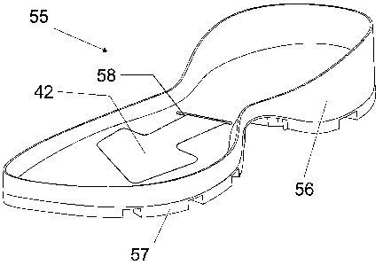
[0050] Referring to Figs. 23 and 24, there is illustrated
the electronic device 42 as positioned in a sole 55 of a
footwear item. The sole 55 has a midsole 56 that is
relatively insulated (e.g., an electrical resistance being
over 35,000,000 ohms according to test method ASTM F2413-05 is
well suited for the midsole 56) . The outsole 57 is at a
bottom of the midsole 56 and is relatively conductive or has
parts that are relatively conductive (e.g., an electrical
resistance being below 500,000 ohms according to test method
ASTM F2413-05 is well suited for the outsole 57) . A slot 58
is defined in the midsole 56 and allows a portion of the first
flexible substrate portion 43 to pass therethrough so as to
have a major portion of the electronic device 42 on a bottom
side of the midsole 56, and therefore in contact with the
outsole 57. As shown in Fig. 24, there may be defined a
cavity in the midsole 56 so as to accommodate the body 45 of
the electronic device 42. Considering that the substrate
portions 43 and 44 are flexible, they have a tendency to
remain in contact with the foot of the wearer, thereby
insuring that there remains a conductive path between the foot
of the wearer and the electronic device 42.
Description of an embodiment of the printed circuit
[0051] Referring to Fig. 18 and 19, an example of suitable
printed circuit is shown at 35 in the form of a printed
circuit board, and has a top contact plate 36, small signal
transistor 37, resistor 38, small signal transistor 39. A
hole 40 in the printed circuit 35 allows electrical contact
between the circuit and a bottom contact plate 41.
[0052] The small signal transistors 37 and 39 may operate
in a depletion mode, and may be SIPMOS, by Infineon #BSS126,
-11-
CA 02715721 2010-09-29
among other possibilities. The resistor 38 may be a SEI
# RMCF 1/16 6K04 1% TR, among other possibilities.
[0053] The electronic devices described herein improve the
functioning and long-term reliability of safety footwear by
protecting printed circuits and electronic components. The
thermoplastic hotmelt molding material offers thermal
stability and physical protection against impact shocks,
weight compressions and flexions. It also offers a high level
of electrical insulation, resisting in some cases a tension of
18,000 Volts with a 1 mm thickness.
[0054] Moreover, the electronic devices described herein
reduce problems due to hydrolysis by sealing the printed
circuits and electronic components. The injection process of
the thermoplastic hotmelt molding material assures that
components stay dry and protected from humidity.
[0055] The electronic devices described herein also provide
a solution to reduce the risk of destruction of electronic
components in situation of high voltage alternative current
discharge. The thermoplastic hotmelt molding material
electrically insulates all parts of the disclosed electronic
device, significantly reducing the risk of electrical "short"
or "arc" from one conductive part to an other (for example:
from the top conductive elastomer insert 7 to the small
cylinder 16 of the sole, as in Fig. 10). High voltage
alternative current may be highly hazardous to human.
Consequently, footwear incorporating electrical devices must
be designed to assure enhanced safety.
[0056] The electronic devices described herein provides a
reliable solution to comply with standards on protective
footwear incorporating electronic components like resistors,
and simplifies the integration of electrical devices into
footwear by shoe manufacturers. The shape of the disclosed
electronic device makes it easier for manufacturers of
footwear to assure a good electrical contact from the top
-12-
CA 02715721 2010-09-29
layers (insole, construction board) of the shoe to the top
contact plate (10) of the electronic device and from the
bottom contact plate (5) to the conductive zones (17) of the
outsole.
[0057] The novel method of assembly simplifies the
integration of electrical devices into footwear by shoe
manufacturers. The method ensures a reliable electrical
connection between the top layers (insole, construction board)
of the shoe and the top interface 2 of the electronic device.
The method also ensures a reliable electrical connection
between the bottom contact plate 5 of the electronic device
and the conductive zones 17 of the outsole, and provides an
efficient dissipative performance without sacrificing the
"non-marking" and other important physical properties of the
outsole.
-13-