Sélection de la langue

Search

Sommaire du brevet 2716943 

Énoncé de désistement de responsabilité concernant l'information provenant de tiers

Une partie des informations de ce site Web a été fournie par des sources externes. Le gouvernement du Canada n'assume aucune responsabilité concernant la précision, l'actualité ou la fiabilité des informations fournies par les sources externes. Les utilisateurs qui désirent employer cette information devraient consulter directement la source des informations. Le contenu fourni par les sources externes n'est pas assujetti aux exigences sur les langues officielles, la protection des renseignements personnels et l'accessibilité.

Disponibilité de l'Abrégé et des Revendications

L'apparition de différences dans le texte et l'image des Revendications et de l'Abrégé dépend du moment auquel le document est publié. Les textes des Revendications et de l'Abrégé sont affichés :

  • lorsque la demande peut être examinée par le public;
  • lorsque le brevet est émis (délivrance).
(12) Demande de brevet: (11) CA 2716943
(54) Titre français: CIRCUIT INTEGRE SPECIFIQUE A UNE APPLICATION COMPLEMENTAIRE POUR DES LAMPES FLUORESCENTES COMPACTES
(54) Titre anglais: COMPLIMENTARY APPLICATION SPECIFIC INTEGRATED CIRCUIT FOR COMPACT FLUORESCENT LAMPS
Statut: Réputée abandonnée et au-delà du délai pour le rétablissement - en attente de la réponse à l’avis de communication rejetée
Données bibliographiques
(51) Classification internationale des brevets (CIB):
  • H05B 41/282 (2006.01)
  • H01L 27/06 (2006.01)
  • H02M 07/538 (2007.01)
(72) Inventeurs :
  • NERONE, LOUIS R. (Etats-Unis d'Amérique)
(73) Titulaires :
  • GENERAL ELECTRIC COMPANY
(71) Demandeurs :
  • GENERAL ELECTRIC COMPANY (Etats-Unis d'Amérique)
(74) Agent: CRAIG WILSON AND COMPANY
(74) Co-agent:
(45) Délivré:
(86) Date de dépôt PCT: 2009-01-23
(87) Mise à la disponibilité du public: 2009-09-11
Licence disponible: S.O.
Cédé au domaine public: S.O.
(25) Langue des documents déposés: Anglais

Traité de coopération en matière de brevets (PCT): Oui
(86) Numéro de la demande PCT: PCT/US2009/031856
(87) Numéro de publication internationale PCT: US2009031856
(85) Entrée nationale: 2010-08-26

(30) Données de priorité de la demande:
Numéro de la demande Pays / territoire Date
12/044,150 (Etats-Unis d'Amérique) 2008-03-07

Abrégés

Abrégé français

Linvention porte sur un ballast d'éclairage dans lequel il y a typiquement plusieurs composants discrets qui se combinent pour prendre un signal en courant alternatif externe et le convertir en un signal en courant continu, et à nouveau en un signal en courant alternatif pour alimenter une lampe. Plusieurs de ces composants peuvent être reçus sur un circuit intégré spécifique à une application. Par le placement de transistors de commutation (20, 22), leurs diodes associées (34, 36) et un circuit de redressement (52) sur un circuit intégré monolithique (60), le circuit de ballast est globalement rendu plus fiable et plus robuste et peut être fabriqué à un coût inférieur que si des composants discrets avaient été utilisés.


Abrégé anglais


In a lighting ballast there are typically several discrete components that
combine to take an external AC signal and
convert it to a DC signal, and back to an AC signal for powering a lamp.
Several of these components can be housed on an application
specific integrated circuit. By placing switching transistors (20, 22) their
companion diodes (34, 36), and a rectifying circuit
(52) on a monolithic integrated circuit (60), the ballast circuit as a whole
is made more reliable and robust and can be
manufactured at a lower cost than if discrete components had been used.

Revendications

Note : Les revendications sont présentées dans la langue officielle dans laquelle elles ont été soumises.


WHAT IS CLAIMED IS:
1. A lighting ballast circuit comprising:
a lamp portion that has contacts for receiving a light source;
an integrated circuit including:
a first transistor;
a second transistor in series with the first transistor, the first
and second transistors being conductive in alternating cycles,
a first diode in an anti-parallel combination with the first
transistor that substantially diminishes reverse current flow through the
first transistor,
a second diode in an anti-parallel combination with the
second transistor that substantially diminishes reverse current flow
through the second transistor; and
a drive portion configured to supply drive signals to the integrated circuit.
2. The lighting ballast circuit as set forth in claim 1, wherein the
integrated
circuit further includes:
a rectifier for converting alternating current from a voltage source to direct
current and providing the direct current to the first and second transistors.
3. The lighting ballast as set forth in claim 2, wherein the rectifier is a
full
wave rectifier.
4. The lighting ballast as set forth in claim 2, wherein the rectifier
supplies a
bus signal of substantially 450 Volts.
5. The lighting ballast as set forth in claim 1, wherein the integrated
circuit is
monolithic.
6. The lighting ballast as set forth in claim 1, wherein the integrated
circuit
further includes:
7

at least one starting resistor that prevents current in the ballast circuit
from
exceeding tolerable levels during startup.
7. The lighting ballast as set forth in claim 1, wherein the transistors are
bipolar junction transistors.
8. The lighting ballast as set forth in claim 7, wherein the integrated
circuit
further includes:
contacts to accept an AC signal from an external AC voltage source;
contacts to connect to positive and negative circuit buses;
a contact connected to emitters of the transistors; and
a contact connected to bases of the transistors.
9. An integrated circuit comprising:
a first transistor;
a second transistor in series with the first transistor;
a first diode in an anti-parallel combination with the first transistor that
substantially diminishes reverse current flow through the first transistor;
a second diode in an anti-parallel combination with the second transistor
that substantially diminishes reverse current flow through the second
transistor.
10. The integrated circuit as set forth in claim 9, wherein the transistors
and
diodes are printed on a monolithic substrate.
11. The integrated circuit as set forth in claim 9, wherein the first and
second
transistors are bipolar junction transistors.
12. The integrated circuit as set forth in claim 11, further including:
first and second contacts that are connected to an external AC voltage
source;
a third contact that is connected to a positive bus rail;
a fourth contact that is connected to a negative bus rail
a fifth contact that is connected to bases of the first and second
transistors;
8

a sixth contact that is connected to emitters of the first and second
transistors.
13. The integrated circuit as set forth in claim 9, further including:
a rectifier for converting an AC input signal to a DC voltage signal and
providing the DC voltage signal to the first and second transistors.
14. The integrated circuit as set forth in claim 9, wherein the rectifier is a
full
wave bridge rectifier.
15. A method of manufacturing a monolithic integrated circuit comprising:
placing first and second bipolar junction transistors in a series relationship
with respective emitters connected at a first contact and respective bases
connected at a
second contact;
placing a first diode in an anti-parallel relationship with the first
transistor,
connected with a positive bus voltage;
placing a second diode in an anti-parallel relationship with the second
transistor, connected with a negative bus voltage.
16. The method as set forth in claim 15, further including:
placing a rectifier between the transistors and an external AC voltage
source for converting an AC signal from the external AC source into a DC
signal for the
transistors.
17. The method as set forth in claim 16, wherein the rectifier is a full wave
rectifier.
18. The method as set forth in claim 15, further including:
placing a first startup resistor between the positive bus voltage and the
bases of the transistors; and
placing a second startup resistor in parallel with the second diode.
19. A method of powering a lamp comprising:
providing a first AC signal to a monolithic integrated circuit;
9

converting the first AC signal into a DC signal with a rectifier resident on
the integrated circuit;
converting the DC signal into a second AC signal with first and second
transistors resident on the integrated circuit; and
protecting the transistors with diodes integrated into the integrated circuit
in anti-parallel relationships with the transistors; and,
providing the second AC signal to a lamp with the integrated circuit.

Description

Note : Les descriptions sont présentées dans la langue officielle dans laquelle elles ont été soumises.


CA 02716943 2010-08-26
WO 2009/111110 PCT/US2009/031856
COMPLIMENTARY APPLICATION SPECIFIC
INTEGRATED CIRCUIT FOR COMPACT
FLUORESCENT LAMPS
BACKGROUND OF THE INVENTION
[0001] The present invention relates to lamp ballasts. It finds particular
application in simplifying lamp ballast circuitry through the use of
application specific
integrated circuits (ASICs) and will be described with particular reference
thereto. It is to
be appreciated, however, that the present invention is also applicable to
other circuits as
well as lamp ballasts, and is not limited to the aforementioned application.
[0002] Typical lamp ballasts driven off of a direct current (DC) bus signal
include
a pair of transistors that convert the DC signal to an alternating current
(AC) signal for
driving a lamp operably connected to the ballast. This is typically done with
similar
transistors such as bipolar junction transistors (BJTs), and will include a
base drive
transformer and a diac starting circuit. Such a circuit topology is described
in U.S.
Patent No. 6,847,175, issued January 25, 2005 to Nerone, which is incorporated
by
reference herein in its entirety.
BRIEF DESCRIPTION OF THE INVENTION
[0003] In accordance with one aspect, a lighting ballast circuit is provided.
The ballast includes a lamp portion that has contacts for receiving a light
source.
The ballast also includes an integrated circuit. The integrated circuit
includes a
first transistor and a second transistor in series with the first transistor,
the first
and second transistors being conductive in alternating periods of time. A
first
diode sits in an anti-parallel combination with the first transistor and
substantially
diminishes reverse current flow through the first transistor. A second diode
sits in
an anti-parallel combination with the second transistor and substantially
diminishes reverse current flow through the second transistor. A drive portion
supplies drive signals to the integrated circuit.
[0004] In accordance with another aspect, an integrated circuit is
provided. A first transistor and a second transistor are in series with each
other.
1

CA 02716943 2010-08-26
WO 2009/111110 PCT/US2009/031856
A first diode sits in an anti-parallel combination with the first transistor
and
substantially diminishes reverse current flow through the first transistor. A
second diode sits in an anti-parallel combination with the second transistor
and
helps prevent reverse current flow through the second transistor.
[0005] In accordance with another aspect, a method of manufacturing a
monolithic integrated circuit is provided. First and second bipolar junction
transistors are placed in a series relationship with respective emitters
connected at
a first contact and respective bases connected at a second contact. A first
diode is
placed in an anti-parallel relationship with the first transistor, connected
with a
positive bus voltage. A second diode is placed in an anti-parallel
relationship
with the second transistor, connected with a negative bus voltage.
[0006] In accordance with another aspect, a method of powering a lamp
is disclosed. A first AC signal is provided to a monolithic integrated
circuit. The
first AC signal is converted into a DC signal by a rectifier integrated into
the
integrated circuit. The DC signal is converted into a second AC signal with
first
and second transistors resident on the integrated circuit. The transistors are
protected by diodes integrated into the integrated circuit in anti-parallel
relationships with the transistors. The second AC signal is provided to a lamp
with the integrated circuit.
BRIEF DESCRIPTION OF THE DRAWINGS
[0007] The invention may take form in various components and arrangements of
components, and in various steps and arrangements of steps. The drawings are
only for
purposes of illustrating preferred embodiments and are not to be construed as
limiting the
invention.
[0008] FIGURE 1 is a circuit diagram of a ballast circuit with components
indicated that are included on an ASIC;
[0009] FIGURE 2 is a circuit diagram of an ASIC that takes the place of the
components indicated in FIGURE 1
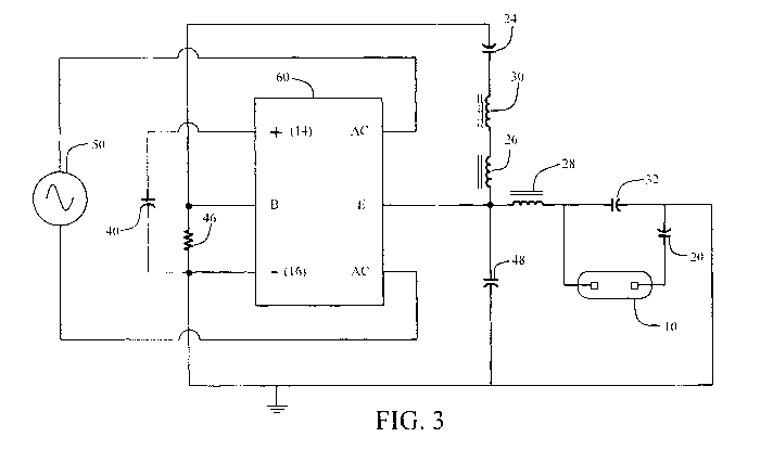
[0010] FIGURE 3 is a depiction of the ballast circuit of FIGURE 1 with the
ASIC
of FIGURE 2 substituted for the indicated components in FIGURE 1.
2

CA 02716943 2010-08-26
WO 2009/111110 PCT/US2009/031856
DETAILED DESCRIPTION OF THE INVENTION
[0011] With reference to FIGURE 1, a light source 10 is operably connected
between contacts 12, of a ballast circuit 13. In one embodiment, the circuit
13 has a DC
bus rail 14. The DC bus rail 14 can have a potential on the order of 450 V.
The circuit 13
is referenced at point 16 to ground. The light source 10 is preferably a
fluorescent lamp
that operates at a particular frequency or range of frequencies. A DC blocking
capacitor
18 is included between the lamp and ground. The ballast circuit provides AC
power at
the operational frequency of the lamp.
[0012] In order to convert a DC signal into an AC signal, a first transistor
20 and
a second transistor 22 alternate between periods of conductivity and periods
of non-
conductivity, out of phase with each other. That is, when the first transistor
20 is
conductive, the second transistor 22 is non-conductive, and vice-versa. The
action of
alternating periods of conduction of the transistors provides an AC signal
across the
contacts 12. In one embodiment, the first transistor is a 13003 type
transistor, and the
second transistor is a 93003 type transistor.
[0013] Each transistor 20, 22 has a respective base and emitter. The voltage
from
base to emitter on either transistor defines the conduction state of that
transistor. That is,
the base-to-emitter voltage of transistor 20 defines the conductivity of
transistor 20 and
the base-to-emitter voltage of transistor 22 defines the conductivity of
transistor 22. As
shown, the emitters of the two transistors 20, 22 are connected at a common
node E. The
bases of the transistors 20, 22 are connected at a control node B. The single
voltage
between the control node B and the common node E determines the conductivity
of both
transistors 20, 22. The collectors of the transistors 20, 22 are connected to
the bus voltage
14 and ground 16, respectively.
[0014] A gate drive circuit, connected between the common node E and the
control node B controls the conduction states of the transistors 20, 22. The
gate drive
circuit includes a serial capacitor 24, and a drive inductor 26 that is
connected to a
resonant inductor 28 at the common node E. The other end of the drive inductor
26 is
coupled to a phase inductor 30. The phase inductor 30 is used to adjust the
phase angle of
the base-emitter voltage appearing between nodes E and B. The drive inductor
26
3

CA 02716943 2010-08-26
WO 2009/111110 PCT/US2009/031856
provides a driving energy for the operation of the drive circuit. The resonant
inductor 28
along with a resonant capacitor 32 connected between nodes 14 and 18 determine
the
operating frequency of the lamp 10. The serial capacitor 24 charges to provide
sufficient
voltage to turn the first transistor 20 conductive. During steady state
operation of the
ballast, the serial capacitor 24 aids in switching between the two transistors
20, 22.
[0015] In one embodiment, when one transistor is conductive, the other is non-
active or non-conductive. That is, there are no periods of time when both
transistors are
operative or conductive. To substantially diminish current flow in a reverse
direction
through the first transistor 20 while the second transistor 22 is conductive,
a first diode 34
is included in the circuit in an anti-parallel relationship with respect to
the first transistor
20. The first diode 34 provides a current shunt that redirects current from
flowing in a
reverse direction across the first transistor 20. Similarly, a second diode 36
is disposed in
an anti-parallel relationship with the second transistor 22 that substantially
diminishes
current flow in a reverse direction across the second transistor 22 while the
first transistor
20 is conductive. Preferably, the diodes 34, and 36 are PIN diodes. PIN diodes
have an
intrinsic semi-conducting region between a p-doped region and an n-doped
region. In one
embodiment, the diodes used are 1N4004 type diodes. It is to be appreciated,
of course,
that other diodes having the required characteristics may also be used.
[0016] Additionally, the ballast circuit includes a smoothing capacitor 40
between
the bus voltage 14 and ground 16 to smooth abnormalities and noise in the bus
voltage
signal. Starting resistors 42, 44, 46 prevent current in the ballast circuit
from exceeding
tolerable levels during startup, before the capacitors and inductors are
charged. A so-
called snubbing capacitor 48 is located between the node E and ground 16.
[0017] An alternating current source 50 provides power to the ballast. The AC
signal is converted to a DC signal by a rectifier 52. The rectifier 52 shown
in FIGURE 1
is a full wave rectifier that includes four diodes 52a, 52b, 52c, and 52d.
Alternately, a
half-wave rectifier could also be used. Additional smoothing and shaping
circuitry is also
contemplated. As mentioned previously, the AC source 50 and the rectifier 52
combine
to provide a DC signal on the order of substantially 450 Volts, but certainly
other
potentials are possible depending on the intended application.
4

CA 02716943 2010-08-26
WO 2009/111110 PCT/US2009/031856
[0018] The circuit of FIGURE 1 can be simplified to provide a ballast that
performs the same function, but is easier and less expensive to manufacture,
and more
robust and resistant to failure. The dashed lines in FIGURE 1 represent
portions of the
ballast that are included in an application specific integrated circuit
(ASIC). FIGURE 2
shows the circuit topology of an ASIC 60 that includes the indicated
components of
FIGURE 1. In FIGURE 2, like components are given the same reference numerals
as
FIGURE 1. As shown in the embodiment of FIGURE 2, the ASIC 60 is a six pin
chip.
Two pins are connected to the AC power source. One pin is connected to the
circuit bus
14, and one pin is connected to circuit ground 16. The remaining two pins
represent
nodes E and B, that is, the base and emitter nodes. Optionally, the rectifier
52 could be
external, and does not necessarily have to be housed on the ASIC 60.
Additional circuitry
such as voltage clamps, protective diodes, and the like, could also be
included on the
ASIC 60. Of course, the ASIC 60 could have more pins, and the ASIC 60 could
carry
additional circuitry, such as end-of-life testing circuitry,
monitoring/diagnostic circuitry,
or the like.
[0019] FIGURE 3 depicts the circuit of FIGURE 1, with the ASIC 60 in place.
Again, like components are indicated with like reference numerals.
[0020] In the illustrated embodiment, the ASIC 60 is a monolithic unit. This
has
the advantage of replacing the discrete circuit components and housing them on
a single
crystal substrate. By taking the discrete complimentary pair of transistors,
and their
associated starting resistors and companion diodes, the overall cost of the
ballast is
decreased, and reliability is increased. Additionally, the ballast does not
take up as much
physical space upon being implemented into a product.
[0021 ] Exemplary component values for the ballast circuit are as follows:
Part Description Part Number Nominal Value
Lamp 10 23 watts
DC Bus Voltage 14 450 Volts
Circuit Reference 16 0 Volts
DC Blocking Capacitor 18 47 of
First Transistor 20 13003
Second Transistor 22 93003

CA 02716943 2010-08-26
WO 2009/111110 PCT/US2009/031856
Drive Inductor 26 360 H
Resonant Inductor 28 3.6 mH
Phase Inductor 30 150 H
Resonant Capacitor 32 1.5 of
First Diode 34 1N4004
Second Diode 36 1N4004
Smoothing Capacitor 40 220 of
Starting Resistor 42 560 kf2
Starting Resistor 44 560 kf2
Starting Resistor 46 560 kf2
Snubbing Capacitor 48 120 pf
[0022] The invention has been described with reference to the preferred
embodiment. Modifications and alterations will occur to others upon a reading
and
understanding of the preceding detailed description. It is intended that the
invention be
construed as including all such modifications and alterations insofar as they
come within
the scope of the appended claims or the equivalents thereof.
6

Dessin représentatif
Une figure unique qui représente un dessin illustrant l'invention.
États administratifs

2024-08-01 : Dans le cadre de la transition vers les Brevets de nouvelle génération (BNG), la base de données sur les brevets canadiens (BDBC) contient désormais un Historique d'événement plus détaillé, qui reproduit le Journal des événements de notre nouvelle solution interne.

Veuillez noter que les événements débutant par « Inactive : » se réfèrent à des événements qui ne sont plus utilisés dans notre nouvelle solution interne.

Pour une meilleure compréhension de l'état de la demande ou brevet qui figure sur cette page, la rubrique Mise en garde , et les descriptions de Brevet , Historique d'événement , Taxes périodiques et Historique des paiements devraient être consultées.

Historique d'événement

Description Date
Le délai pour l'annulation est expiré 2015-01-23
Demande non rétablie avant l'échéance 2015-01-23
Réputée abandonnée - omission de répondre à un avis sur les taxes pour le maintien en état 2014-01-23
Inactive : Abandon.-RE+surtaxe impayées-Corr envoyée 2014-01-23
Inactive : Page couverture publiée 2010-12-01
Inactive : Notice - Entrée phase nat. - Pas de RE 2010-11-01
Inactive : CIB attribuée 2010-10-27
Demande reçue - PCT 2010-10-27
Inactive : CIB en 1re position 2010-10-27
Inactive : CIB attribuée 2010-10-27
Exigences pour l'entrée dans la phase nationale - jugée conforme 2010-08-26
Demande publiée (accessible au public) 2009-09-11

Historique d'abandonnement

Date d'abandonnement Raison Date de rétablissement
2014-01-23

Taxes périodiques

Le dernier paiement a été reçu le 2013-01-02

Avis : Si le paiement en totalité n'a pas été reçu au plus tard à la date indiquée, une taxe supplémentaire peut être imposée, soit une des taxes suivantes :

  • taxe de rétablissement ;
  • taxe pour paiement en souffrance ; ou
  • taxe additionnelle pour le renversement d'une péremption réputée.

Les taxes sur les brevets sont ajustées au 1er janvier de chaque année. Les montants ci-dessus sont les montants actuels s'ils sont reçus au plus tard le 31 décembre de l'année en cours.
Veuillez vous référer à la page web des taxes sur les brevets de l'OPIC pour voir tous les montants actuels des taxes.

Historique des taxes

Type de taxes Anniversaire Échéance Date payée
Taxe nationale de base - générale 2010-08-26
TM (demande, 2e anniv.) - générale 02 2011-01-24 2010-12-31
TM (demande, 3e anniv.) - générale 03 2012-01-23 2012-01-03
TM (demande, 4e anniv.) - générale 04 2013-01-23 2013-01-02
Titulaires au dossier

Les titulaires actuels et antérieures au dossier sont affichés en ordre alphabétique.

Titulaires actuels au dossier
GENERAL ELECTRIC COMPANY
Titulaires antérieures au dossier
LOUIS R. NERONE
Les propriétaires antérieurs qui ne figurent pas dans la liste des « Propriétaires au dossier » apparaîtront dans d'autres documents au dossier.
Documents

Pour visionner les fichiers sélectionnés, entrer le code reCAPTCHA :


Pour visualiser une image, cliquer sur un lien dans la colonne description du document. Pour télécharger l'image (les images), cliquer l'une ou plusieurs cases à cocher dans la première colonne et ensuite cliquer sur le bouton "Télécharger sélection en format PDF (archive Zip)" ou le bouton "Télécharger sélection (en un fichier PDF fusionné)".

Liste des documents de brevet publiés et non publiés sur la BDBC .

Si vous avez des difficultés à accéder au contenu, veuillez communiquer avec le Centre de services à la clientèle au 1-866-997-1936, ou envoyer un courriel au Centre de service à la clientèle de l'OPIC.


Description du
Document 
Date
(aaaa-mm-jj) 
Nombre de pages   Taille de l'image (Ko) 
Abrégé 2010-08-25 1 63
Revendications 2010-08-25 4 113
Dessins 2010-08-25 3 106
Description 2010-08-25 6 273
Dessin représentatif 2010-08-25 1 18
Rappel de taxe de maintien due 2010-10-31 1 114
Avis d'entree dans la phase nationale 2010-10-31 1 207
Rappel - requête d'examen 2013-09-23 1 118
Courtoisie - Lettre d'abandon (requête d'examen) 2014-03-19 1 164
Courtoisie - Lettre d'abandon (taxe de maintien en état) 2014-03-19 1 171
PCT 2010-08-25 11 425