Note : Les descriptions sont présentées dans la langue officielle dans laquelle elles ont été soumises.
CA 02721714 2010-10-15
WO 2009/129500 PCT/US2009/041024
1
ENHANCED TRIM RESOLUTION VOLTAGE-CONTROLLED DIMMING LED
DRIVING CIRCUIT
TECHNICAL FIELD
[0001] The present disclosure is directed, in general, to
voltage-controlled dimming illuminated displays and, more
specifically, to pushbutton switch displays illuminated by
voltage-controlled dimming light emitting diodes.
BACKGROUND
[0002] The crewstation instrumentation panels for
commercial and military aircraft, naval vessels and tracked
and armored vehicles, like many other display systems,
frequently employ illuminated indicators and controls (e.g.,
pushbutton switches) . A voltage controlled dimming driver
circuit for light emitting diode (LED) illuminated switches
[0003] Pushbutton switches with voltage-controlled dimming
light emitting diode driver circuits are described, for
example, in U.S. Patents Nos. 5,929,568, 6,323,698, 6,489,728,
6,650,064, 6,653,798, 6,670,776, 6,737,814, 7,126,290,
7,157,859, and 7,202,608, the content of all of which are
incorporated herein by reference. However, many of the
designs disclosed therein suffer from power inefficiencies,
particularly at high applied input voltages. In addition,
none of the designs allow operation based on direct current
(DC) applied input voltages of either polarity.
[0004] There is, therefore, a need in the art for improved
power efficiency and dual polarity operation in a voltage-
controlled dimming light emitting diode driver circuit.
CA 02721714 2010-10-15
WO 2009/129500 PCT/[TS2009/041024
2
SUMMARY
[0005] To address the above-discussed deficiencies of the
prior art, it is a primary object of the present disclosure to
provide, for use in LED-illuminated pushbutton switch
displays, a plurality of driver circuits for a six-by-four
array of light emitting diodes each switching three pairs of
the light emitting diodes between series connection and
parallel connection based on changes to an applied input
voltage. Driving six light emitting diodes instead of only
four allows illumination of a larger area and improves power
efficiency at higher applied input voltages, while retaining
dimming compatibility at low voltage levels. Each driver
circuit also includes a rectifier allow illumination of the
pushbutton switch with direct current voltages of either
polarity. The quiescent current limiting resistance is split
into multiple resistors for further improved power efficiency.
Each driver circuit also includes a bridge rectifier to allow
illumination of the pushbutton switch with direct current
voltages of either polarity or alternating current voltages.
[0006] The foregoing has outlined rather broadly the
features and technical advantages of the present invention so
that those skilled in the art may better understand the
detailed description of the invention that follows.
Additional features and advantages of the invention will be
described hereinafter that form the subject of the claims of
the invention. Those skilled in the art will appreciate that
they may readily use the conception and the specific
embodiment disclosed as a basis for modifying or designing
other structures for carrying out the same purposes of the
present invention. Those skilled in the art will also realize
that such equivalent constructions do not depart from the
spirit and scope of the invention in its broadest form.
CA 02721714 2010-10-15
WO 2009/129500 PCT/US2009/041024
3
[0007] Before undertaking the DETAILED DESCRIPTION below,
it may be advantageous to set forth definitions of certain
words or phrases used throughout this patent document: the
terms "include" and "comprise," as well as derivatives
thereof, mean inclusion without limitation; the term "or" is
inclusive, meaning and/or; the phrases "associated with" and
"associated therewith," as well as derivatives thereof, may
mean to include, be included within, interconnect with,
contain, be contained within, connect to or with, couple to or
with, be communicable with, cooperate with, interleave,
juxtapose, be proximate to, be bound to or with, have, have a
property of, or the like; and the term "controller" means any
device, system or part thereof that controls at least one
operation, whether such a device is implemented in hardware,
firmware, software or some combination of at least two of the
same. It should be noted that the functionality associated
with any particular controller may be centralized or
distributed, whether locally or remotely. Definitions for
certain words and phrases are provided throughout this patent
document, and those of ordinary skill in the art will
understand that such definitions apply in many, if not most,
instances to prior as well as future uses of such defined
words and phrases.
CA 02721714 2010-10-15
WO 2009/129500 PCTIUS2009/041024
4
BRIEF DESCRIPTION OF THE DRAWINGS
[0008] For a more complete understanding of the present
invention, and the advantages thereof, reference is now made
to the following descriptions taken in conjunction with the
accompanying drawings, wherein like numbers designate like
objects, and in which:
[0009] FIGURE 1 is a perspective assembled view of a
voltage-controlled dimming light emitting diode illuminated
display pushbutton switch according to one embodiment of the
present disclosure;
[0010] FIGURE 2 is a diagram illustrating the array of
light emitting diodes within a voltage-controlled dimming
light emitting diode illuminated display pushbutton switch
according to one embodiment of the present disclosure;
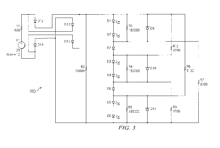
[0011] FIGURE 3 is a circuit diagram for a voltage-
controlled dimming light emitting diode driver circuit
employed within a voltage-controlled dimming light emitting
diode illuminated display pushbutton switch according to one
embodiment of the present disclosure; and
[0012] FIGURES 4 and 5 are voltage dimming curves of
luminance as a function of voltage for the voltage-controlled
dimming light emitting diode driver circuit of FIGURE 3.
CA 02721714 2010-10-15
WO 2009/129500 PCT/US2009/041024
DETAILED DESCRIPTION OF THE INVENTION
[0013] FIGURE 1 through 5, discussed below, and the various
embodiments used to describe the principles disclosed in this
patent document are by way of illustration only and should not
5 be construed in any way to limit the scope of the invention.
Those skilled in the art will understand that the principles
of the present invention may be implemented in any suitably
arranged device.
[00141 FIGURE 1 is a perspective assembled view of a
voltage-controlled dimming light emitting diode illuminated
display pushbutton switch according to one embodiment of the
present disclosure. Pushbutton switch 100 includes a voltage-
controlled dimming, light emitting diode illuminated display
that is implemented in largely the same manner as the switch
disclosed in U.S. Patent No. 6,653,798, the content of which
is incorporated herein by reference. For clarity and
simplicity, the complete structure and operation of pushbutton
switch 100 is not depicted or described herein. Instead, only
so much of the structure and operation of a pushbutton switch
as is unique to the present disclosure and/or necessary for an
understanding of the present disclosure is depicted and
described. Moreover, the principles disclosed herein may be
employed in conjunction with other types of illuminated
displays, including but not limited to indicators and
annunciators.
[0015) Illuminated pushbutton switch 100 includes a switch
housing 101 receiving a switch cap 102 having a display
surface 103 on which illuminated legends are visible, and
which is pressed to actuate the switch. Pushbutton switch cap
housing 101 receives an array of light emitting diodes within
a lamp mount, which also contains the driver circuits for
voltage-controlled dimming of the light emitting diodes, with
CA 02721714 2010-10-15
WO 2009/129500 PCT/US2009/041024
6
contacts (not shown) provided for making electrical connection
to receive a voltage for driving the light emitting diodes.
[0016] The legend plate for display surface 103 may contain
four separate legends visible on the display surface 103 in
each of four quadrants, two legends (each in one half), three
legends (one in one half and two each in one of the remaining
two quadrants) or a single legend. Different quadrants or
different halves may be illuminated in different colors on the
display surface 103.
[0017] FIGURE 2 is a diagram illustrating the array of
light emitting diodes within a voltage-controlled dimming
light emitting diode illuminated display pushbutton switch
according to one embodiment of the present disclosure. One
difference between pushbutton switch 100 and the switch
disclosed in U.S. Patent No. 6,653,798 is that a 6X4 array 200
of twenty-four light emitting diodes is employed, rather than
a 4X4 array. As a result, the display surface 103 and the
switch 100 have a width greater than the respective height.
In addition, the switch housing for illuminated pushbutton
switch 100 is larger, with more space for additional
electrical components within the driver circuits as described
in further detail below.
(0018] The 6X4 array of light emitting diodes may be
logically divided into four quadrants, with the 3X2 sub-array
of light emitting diodes within each particular quadrant
driven as a group so that all light emitting diodes within a
quadrant are either on or off. Each quadrant thus employs a
separate voltage-controlled dimming driver circuit, described
in further detail below. Alternatively, however, the array
may instead be logically divided into two halves, or one half
and two quadrants, and light emitting diodes driven by the
same driver circuit may be interleaved across one of the
CA 02721714 2010-10-15
WO 2009/129500 PCT/US2009/041024
7
halves with light emitting diodes driven by another driver
circuit.
[0019] Although light emitting diodes within separate
quadrants are preferably independently switched to turn the
light emitting diodes on or off, the same voltage is applied
to all light emitting diodes that are switched on, in order to
provide uniform voltage-controlled dimming. Moreover, the
driver circuits for each set of six light emitting diodes are
identical and driven by the same control voltage to provide
uniform voltage-controlled dimming.
[0020] To eliminate a bandgap problem resulting from using
different color light emitting diodes and enable uniform
voltage-controlled dimming of different color legends in
illuminated pushbutton switch 100, each quadrant contains the
same type of light emitting diode, having the same bandgap
voltage (and voltage-luminance) characteristic. Light
emitting diodes emitting a broad spectral radiance with a
single bandgap produce a narrow spectral radiance (typically
blue) which is utilized to excite a broad spectral radiance
fluorescence from a rare earth phosphor deposited within the
light emitting diode package (i.e., "white" light emitting
diodes). The combined spectral radiances of the light
emitting diode and the phosphor emissions produce the
appearance of a high color temperature white light source,
with broad spectral radiance capable of producing a wide
variety of colors including red, yellow, blue, green and
white. In the present invention, each light emitting diode
within the array is such a white light emitting diode.
[0021] Different colors of illumination are provided by
filters disposed between light emitting diode array and the
legend plate for the display surface, comprised of acrylic,
polycarbonate, polyester or glass materials, or a combination
thereof. Those filters are selected to produce a specific
CA 02721714 2010-10-15
WO 2009/129500 PCT/US2009/041024
8
chromaticity, as well as a desired luminance at one or more
specific voltages. Through proper selection of the filters,
white light emitting diodes may be employed to produce all
colors desired. The optical filters contain colorants, dyes
and/or pigments known in the art which selectively remove
white light emitting diode spectral radiance to match specific
chromaticity requirements for illuminated pushbutton switch
100 (e.g., red, yellow, white, green or blue). In addition,
the filters may optionally also contain specialized dyes for
absorption of non-visible red or near infra-red spectral
emissions from the white light emitting diodes for the purpose
of producing night vision imaging system (NVIS) compatible
red, yellow, blue or green colors.
[0022) Also, filters may be formed of glass or plastic with
suitable thin-film optical (interference) coatings to remove
the red or near-infrared spectral emissions. Therefore, the
white light emitting diodes may be filtered to produce any
lighted legend color, including the standard aircraft
illumination colors of blue, green, yellow, red and white or
the NVIS colors of NVIS blue, NVIS green A (blue-green), NVIS
green B (green), NVIS yellow (yellow) and NVIS red (orange-
red).
[0023] The filters are also designed to control the output
luminance emitting from the display surface 103 of pushbutton
cap 102 so that colored lighting produced from the white light
emitting diodes will have approximately the same luminance at
a specific voltage, such as 400-500 foot-lamberts (sunlight
readable) at the maximum or full rated operating voltage.
[0024] Each filter within the pushbutton cap 102 may be
selected to produce a different illumination color, so that
adjacent legends are illuminated in different colors on
display surface 103. Since all of the light emitting diodes
are of the same type and have the same bandgap voltage
CA 02721714 2010-10-15
WO 2009/129500 PCT/IJS2009/041024
9
characteristics and the same voltage-luminance
characteristics, all illumination colors will dim uniformly
when the control voltage (a single control voltage,
independent of illumination color) applied to light emitting
diodes is decreased to reduce luminance. Multiple legends
illuminated in at least two different colors on the pushbutton
cap 102 for a single illuminated pushbutton switch 100 will
therefore all dim uniformly as the applied voltage is reduced.
[0025] The filters are held by a filter mount having
openings therethrough for each filter and essentially serving
as a frame holding the four filters (or two or three filters
for different arrangements of legends on display surface 103).
When the illuminated pushbutton switch 100, the switch housing
101 will contain the pushbutton cap, including the pushbutton
cap housing 102, the legend plate(s), filter(s) and filter
mount, the light emitting diode array, and the driver
circuitry for each quadrant.
[0026] FIGURE 3 is a circuit diagram for a voltage-
controlled dimming light emitting diode driver circuit
employed within a multi-color, voltage-controlled dimming,
light emitting diode-illuminated display according to one
embodiment of the present invention. In an exemplary
embodiment, individual but identical driver circuits, each
implemented by circuit 300, are separately employed for each
group of six light emitting diodes within the array.
[0027] Circuit 300 includes six white light emitting diodes
Dl-D6 illuminating one quadrant or half of the pushbutton
switch 100. The light emitting diodes are grouped in series-
connected pairs D1-D2, D3-D4 and D5-D6, each with the same
forward bias orientation, and each have a forward voltage of
between about 3.6 and about 4.0 volts (V) in an exemplary
embodiment. Within each diode pair, the anode of one light
emitting diode D2, D4 and D6 is connected to the cathode of
CA 02721714 2010-10-15
WO 2009/129500 PCT/US2009/041024
the other light emitting diode Dl, D3 and D5, respectively,
within the pair. A switching circuit is also provided within
driving circuit 300 to switch the pairs of light emitting
diodes between series and parallel connection. The switching
5 circuit includes switching diodes D7 and D8, each with a
forward voltage of about 0.6 V (1.2 V total series forward
voltage drop) in an exemplary embodiment. Switching diode D7
is connected between pairs of light emitting diodes D1-D2 and
D3-D4, with the anode of switching diode D7 connected to the
10 cathode of light emitting diode D2 and the cathode of
switching diode D7 connected to the anode of light emitting
diode D3 (i.e., with the same forward bias orientation as
light emitting diode pairs Dl-D2 and D3-D4) . Switching diode
D8 is connected between pairs of light emitting diodes D3-D4
and D5-D6, with the anode of switching diode D8 connected to
the cathode of light emitting diode D4 and the cathode of
switching diode D8 connected to the anode of light emitting
diode D5 (i.e., with the same forward bias orientation as
light emitting diode pairs D3-D4 and D5-D6).
[0028] The switching circuit also includes switching
resistors R6-R7 and R9-RlO. Switching resistor R6 is
connected across light emitting diode pairs Dl-D2 and D3-D4
and switching diodes D7 and D8, with one terminal connected to
the anode of light emitting diode Dl and the other terminal
connected to the cathode of switching diode D8. Switching
resistor R7 is connected across light emitting diode pairs D3-
D4 and DS-D6 and switching diodes D7 and D8, with one terminal
connected to the anode of switching diode D7 and the other
terminal connected to the cathode of light emitting diode D6.
Each of switching resistors R6 and R7 has a resistance of
9,100 S2. Switching resistor R9 is connected across light
emitting diode pair D5-D6 and switching diode D8, with one
terminal connected to the anode of switching diode D8 and the
CA 02721714 2010-10-15
WO 2009/129500 PCT/US2009/041024
11
other terminal connected to the cathode of light emitting
diode D6. Switching resistor R10 is connected across light
emitting diode pair D1-D2 and switching diode D7, with one
terminal connected to the anode of light emitting diode Dl and
the other terminal connected to the cathode of switching diode
D7. Each of switching resistors R9 and R10 has a resistance
of 4,700 Q. The switching circuit formed by switching diodes
D7-D8 and switching resistors R6-R7 and R9-Rl0 switch the
light emitting diode pairs Dl-D2, D3-D4 and D5-D6 between
series-connection and parallel-connection based on changes in
the driving voltage applied to driving circuit 300. When the
voltage across light emitting diodes Dl-D6 and switching
diodes D7-D8 falls below the cumulative forward bias voltages
for those diodes, switching diodes D7-D8 stop conducting and
the three parallel circuit paths are formed consisting of (a)
light emitting diodes Dl-D2 and switching resistance R7, (b)
switching resistance R10, light emitting diodes D3-D4, and
switching resistance R9, and (c) switching resistance R6 and
light emitting diodes D5-D6. As long as the voltage across
light emitting diodes Dl-D6 and switching diodes D7-D8 equals
or exceeds the cumulative forward bias voltages for those
diodes, switching diodes D7-D8 conduct and light emitting
diodes Dl-D6 and switching diodes D7-D8 are all connected in
series.
[0029] Driving circuit 300 also includes quiescent current
limiting resistors R2-R5 and overvoltage protection zener
diodes D9-Dli. Quiescent current limiting resistor R2 is
connected across light emitting diodes D1-D6 and switching
diodes D7-D8, with one terminal connected to the anode of
light emitting diode Dl and the other terminal connected to
the cathode of light emitting diode D6. Quiescent current
limiting resistor R2 has a value of 20,000 0. Quiescent
current limiting resistor R3 is connected across light
CA 02721714 2010-10-15
WO 2009/129500 PCT/US2009/041024
12
emitting diode pair D1-D2, with one terminal connected to the
anode of light emitting diode Dl and the other terminal
connected to the cathode of light emitting diode D2.
Quiescent current limiting resistor R4 is connected across
light emitting diode pair D3-D4, with one terminal connected
to the anode of light emitting diode D3 and the other terminal
connected to the cathode of light emitting diode D4.
Quiescent current limiting resistor R5 is connected across
light emitting diode pair D5-D6, with one terminal connected
to the anode of light emitting diode D5 and the other terminal
connected to the cathode of light emitting diode D6. Each of
the quiescent current limiting resistors R3, R4 and R5 has a
resistance of 180,000 Ohms (0). Zener diode D9 is connected
across light emitting diode pair Dl-D2, with a forward bias
orientation opposite the forward bias orientation of light
emitting diodes D1-D2. Zener diode D10 is connected across
light emitting diode pair D3-D4, with a forward bias
orientation opposite the forward bias orientation of light
emitting diodes D3-D4. Zener diode Dll is connected across
light emitting diode pair D5-D6, with a forward bias
orientation opposite the forward bias orientation of light
emitting diodes D5-D6. When the voltage drop across any of
light emitting diode pairs Dl-D2, D3-D4 or D5-D6 exceeds the
reverse breakdown voltage of a respective one of zener diodes
D9, D10 or D1l, the excess current passes through the zener
diode. In addition, the zener diodes D9-D1l provide a
"layered" protection against failure of two electrically
independent quadrants (the first layer) and against a failure
within a single quadrant (the second layer). In either event,
the remaining operational LEDs of array 200 within switch 100
will continue to illuminate the display surface 103.
[0030] Driving circuit 300 also includes a rectifier formed
by diodes D12-D15. Rectifier diode D12 is connected with a
CA 02721714 2010-10-15
WO 2009/129500 PCT/US2009/041024
13
forward bias orientation between a first input node and a
first terminal of quiescent current limiting resistor R2.
Rectifier diode D13 is connected with a reverse bias
orientation between the first input node and a second terminal
of quiescent current limiting resistor R2. Rectifier diode
D14 is connected with a reverse bias orientation between a
second input node and the second terminal of quiescent current
limiting resistor R2. Rectifier diode D15 is connected with a
forward bias orientation between the second input node and the
first terminal of quiescent current limiting resistor R2.
[0031] Resistor Rl is connected in series between the first
terminal of quiescent current limiting resistor R2 and the
applied input voltage represented in FIGURE 3 by voltage
source V1. Resistor R1 sets the kickover point between
series-connection and parallel-connection as a function of
input voltage applied by a voltage source Vl, and also serves
to limit the current of a transient or overvoltage event and
to limit the operating current to safe levels in order to
prevent a catastrophic failure of the display circuitry.
Voltage source V1 does not form part of driving circuit 300,
but instead merely represents the input voltage applied to the
contacts of the pushbutton switch.
[0032) FIGURES 4 and 5 are voltage dimming curves of
luminance as a function of voltage for the voltage-controlled
dimming light emitting diode driver circuit of FIGURE 3.
FIGURE 4 illustrates the luminance as a function of applied
direct current (DC) input voltage for driver circuit 300 (the
trace on top at the lower end of the voltage range
illustrated) versus the driver circuit for two groups of light
emitting diode pairs (the trace on bottom at the lower end of
the voltage range illustrated) as disclosed in U.S. Patent No.
6,323,598, the content of which is incorporated herein by
reference. As illustrated, splitting the light emitting
CA 02721714 2010-10-15
WO 2009/129500 PCT/US2009/041024
14
diodes into three groups retains dimming compatibility at low
voltage levels. Incorporation of a bridge rectifier (diodes
D12-D15) allows the circuit to operate from either polarity
direct current (DC) as well as alternating current (AC).
FIGURE 5 illustrates the luminance as a function of applied AC
input voltage.
[0033] The driver circuit disclosed herein allows
illumination of a larger physical area, with better power
efficiency at higher applied voltages, than the design
disclosed in U.S. Patent No. 6,323,598. In addition,
splitting the quiescent current limiting resistance into
multiple resistors instead of just a single resistor as
disclosed in U.S. Patent No. 6,489,728, the content of which
is incorporated herein by reference, is more power efficient
at higher applied voltages.
[0034] Although the present invention has been described in
detail, those skilled in the art will understand that various
changes, substitutions, variations, enhancements, nuances,
gradations, lesser forms, alterations, revisions, improvements
and knock-offs of the invention disclosed herein may be made
without departing from the spirit and scope of the invention
in its broadest-form.