Note : Les descriptions sont présentées dans la langue officielle dans laquelle elles ont été soumises.
CA 02730795 2011-02-03
Method for operation of a converter circuit, as well as
an apparatus for carrying out the method
DESCRIPTION
Technical field
The invention relates to the field of power
electronics, and relates in particular to a method for
operation of a converter circuit according to the
preamble of the independent claims.
Prior art
Nowadays, converter circuits are used in a multiplicity
of applications. One converter circuit whose voltage
can be scaled particularly easily is specified in
WO 2007/023064 Al. Figure 1 illustrates a converter
circuit such as this according to the prior art,
although, for the sake of clarity, Figure 1 illustrates
only one phase module of the converter circuit. The
converter circuit therein has one phase module for each
phase, with each phase module comprising a first and a
second sub-converter system, and with the sub-converter
systems being connected in series with one another. The
junction point between the two series-connected sub-
converter systems forms an outlet connection, for
example for an electrical load. Each sub-converter
system comprises at least one two-pole switching cell,
wherein these switching cells are connected in series
with one another when there are a plurality of
switching cells in one sub-converter system. Each two-
pole switching cell has controllable bidirectional
power semiconductor switches with a controlled
unidirectional current-flow direction, and a capacitive
energy store. In Figure 1, each switching cell has two
series-connected controllable bidirectional power
semiconductor switches with a controlled unidirectional
CA 02730795 2011-02-03
- 2 -
current-flow direction, and a capacitive energy store
connected in parallel with the series circuit by the
power semiconductor switches. A converter circuit of
this generic type is also specified in
WO 2007/33852 A2.
Since the converter circuit according to
WO 2007/023064 Al or according to WO 2007/33852 A2
contains weakly damped resonant circuits, consisting of
two or more phase modules, the oscillations which occur
therein must be damped for control-engineering purposes
in the currents through the first and the second sub-
converter systems. In this context, WO 2007/33852 A2
specifies a control method which is based on the
principle of freely selectable time intervals for
switching operations of the controllable bidirectional
power semiconductor switches in the switching cells in
the first and second sub-converter systems.
Description of the invention
The object of the invention is to specify an
alternative method, which has been developed further
from the prior art, for operation of a converter
circuit, by means of which undesirable oscillations and
distortions in currents in first and second sub-
converter systems in the converter circuit can be
actively damped.
This object is achieved by the features of claims 1, 3
and 6. Advantageous developments of the invention are
specified in the dependent claims.
The converter circuit has at least two phase modules,
each phase module comprises a first and a second sub-
converter system, and the sub-converter systems for
each phase module are connected in series with one
another. Each sub-converter system comprises a
plurality of series-connected two-pole switching cells,
CA 02730795 2011-02-03
3 -
and each switching cell has controllable bidirectional
power semiconductor switches with a controlled
unidirectional current-flow direction and a capacitive
energy store. On the basis of the method according to
the invention, the power semiconductor switches in the
switching cells in the first sub-converter system are
controlled by means of one control signal, and the
power semiconductor switches in the switching cells in
the second sub-converter system are controlled by means
of a further control signal. Furthermore, the control
signal for the first sub-converter system is formed
from a reference signal with respect to the voltage
across the first sub-converter system, and the further
control signal for the second sub-converter system is
formed from a reference signal with respect to the
voltage across the second sub-converter system.
According to the invention, the control signal is
additionally formed from a damping signal with respect
to the first sub-converter system, wherein the damping
signal is formed from a measured current through the
first sub-converter system and from a predeterminable
resistance value. Furthermore, the further control
signal is additionally formed from a damping signal
with respect to the second sub-converter system,
wherein the damping signal is formed from a measured
current through the second sub-converter system and
from the predeterminable resistance value.
The effect of the respective damping signal corresponds
to a voltage drop across a non-reactive resistance in
the associated sub-converter system, and therefore
damps the currents through the respectively associated
sub-converter system in a desired manner.
In a further embodiment of the invention, the damping
signal with respect to the first sub-converter system
is additionally formed from a predeterminable reference
current through the first sub-converter system. The
damping signal with respect to the second sub-converter
CA 02730795 2011-02-03
- 4 -
system is additionally formed from a predeterminable
reference current through the second sub-converter
system. Presetting a reference current for the
formation of the respective damping signal
advantageously makes it possible to deliberately damp
specific oscillation components of the currents through
the respective sub-converter system.
In one alternative embodiment of the invention, the
control signal for the first sub-converter system is
formed from a reference signal, which is produced in a
central calculation unit, with respect to the
associated switching cell in the first sub-converter
system. A local calculation unit is provided for each
switching cell in the first sub-converter system,
wherein the reference signal with respect to the
associated switching cell in the first sub-converter
system is transmitted to the local calculation units
for the switching cells in the first sub-converter
system. The control signal is then additionally formed
in each of the local calculation units for the
switching cells in the first sub-converter system from
a damping signal with respect to the associated
switching cell in the first sub-converter system,
wherein the damping signal is formed from a measured
current through the associated switching cell in the
first sub-converter system and from a predeterminable
resistance value. The further control signal for the
second sub-converter system is formed from a reference
signal, which is produced in the central calculation
unit, with respect to the associated switching cell in
the second sub-converter system. Furthermore, a local
calculation unit is provided for each switching cell in
the second sub-converter system, wherein the reference
signal with respect to the associated switching cell in
the second sub-converter system is transmitted to the
local calculation units for the switching cells in the
second sub-converter system. Furthermore, the further
control signal is then additionally formed in each of
CA 02730795 2011-02-03
- 5 -
the local calculation units for the switching cells in
the second sub-converter system from a damping signal
with respect to the associated switching cell in the
second sub-converter system, wherein the damping signal
is formed from a measured current through the
associated switching cell in the second sub-converter
system and from the predeterminable resistance value.
The alternative mentioned above results in the currents
through the sub-converter systems advantageously being
damped in the switching cells. The effect of the
respective damping signal corresponds to a voltage drop
across a non-reactive resistance in each switching
cell, wherein the overall effect corresponds to a
series circuit of non-reactive resistances, thus
resulting in the currents through the respective
switching cells in the associated sub-converter system
being damped in the desired manner. The local
measurement of the currents through the switching cells
makes it possible to furthermore ensure the redundancy
and therefore the availability of the damping even in
the event of a failure of a current measurement, for
example in one switching cell. The local formation of
the control signal furthermore avoids the need for the
normal transmission of the control signal to the
individual switching cells.
In a further embodiment of the invention, the
respective damping signal with respect to the
associated switching cell in the first sub-converter
system is additionally formed from a predeterminable
reference current through the associated switching cell
in the first sub-converter system, and the respective
damping signal with respect to the associated switching
cell in the second sub-converter system is additionally
formed from a predeterminable reference current through
the associated switching cell in the second sub-
converter system. In addition to the advantages already
mentioned above, the presetting of a reference current
CA 02730795 2011-02-03
- 6 -
for the formation of the respective damping signal
advantageously makes it possible to deliberately damp
specific oscillation components of the currents through
the switching cells in the associated sub-converter
system.
In a further alternative of the invention, the control
signal for the first sub-converter system is formed
from a damping reference signal, which is produced in a
central calculation unit, with respect to the voltage
across the first sub-converter system, wherein the
damping reference signal with respect to the voltage
across the first sub-converter system is formed from a
predeterminable reference current through the first
sub-converter system, from a predeterminable resistance
value and from a reference signal with respect to the
voltage across the first sub-converter system. A local
calculation unit is then provided for each switching
cell in the first sub-converter system, wherein the
damping reference signal with respect to the voltage
across the first sub-converter system is transmitted to
the local calculation units for the switching cells in
the first sub-converter system. The control signal is
additionally formed in each of the local calculation
units for the switching cells in the first sub-
converter system from a damping signal with respect to
the associated switching cell in the first sub-
converter system, wherein the damping signal is formed
from a measured current through the associated
switching cell in the first sub-converter system and
from a predeterminable further resistance value.
Furthermore, the further control signal for the second
sub-converter system is formed from a damping reference
signal, which is produced in the central calculation
unit, with respect to the voltage across the second
sub-converter system, wherein the damping reference
signal with respect to the voltage across the second
sub-converter system is formed from a predeterminable
reference current through the second sub-converter
CA 02730795 2011-02-03
- 7 -
system, from the predeterminable resistance value and
from a reference signal with respect to the voltage
across the second sub-converter system. Furthermore, a
local calculation unit is then provided for each
switching cell in the second sub-converter system,
wherein the damping reference signal with respect to
the voltage across the second sub-converter system is
transmitted to the local calculation units for the
switching cells in the second sub-converter system.
Furthermore, the further control signal is additionally
formed in each of the local calculation units for the
switching cells in the second sub-converter system from
a damping signal with respect to the associated
switching cell in the second sub-converter system,
wherein the damping signal is formed from a measured
current through the associated switching cell in the
second sub-converter system and from the
predeterminable further resistance value. With this
alternative of the invention as well, specific
oscillation components of the currents through the
switching cells in the associated sub-converter system
can thus be selectively damped. Furthermore, the
reference current is advantageously not transmitted to
the local calculation units.
These and further objects, advantages and features of
the present invention will become obvious from the
following detailed description of preferred embodiments
of the invention in conjunction with the drawing.
Brief description of the drawings
In the figures:
Figure 1 shows one embodiment of a converter circuit
according to the prior art,
Figure 2 shows a first embodiment of an apparatus for
carrying out the method according to the
CA 02730795 2011-02-03
- 8 -
invention for operation of a converter
circuit,
Figure 3 shows a second embodiment of an apparatus for
carrying out the method according to the
invention for operation of a converter
circuit,
Figure 4 shows a third embodiment of an apparatus for
carrying out the method according to the
invention for operation of a converter
circuit,
Figure 5 shows a fourth embodiment of an apparatus for
carrying out the method according to the
invention for operation of a converter
circuit, and
Figure 6 shows a fifth embodiment of an apparatus for
carrying out the method according to the
invention for operation of a converter
circuit.
The reference symbols used in the drawings and their
meanings are listed in summary form in the list of
reference symbols. In principle, the same parts are
provided with the same reference symbols in the
figures. The described embodiments represent examples
of the subject matter according to the invention, and
have no restrictive effect.
Approaches to implementation of the invention
As was already mentioned initially, Figure 1 shows one
embodiment of a converter circuit according to the
prior art. In general, the converter circuit has at
least two phase modules 4, wherein each phase module 4
comprises a first and a second sub-converter system 1,
2, and the sub-converter systems 1, 2 for each phase
CA 02730795 2011-02-03
- 9 -
module 4 are connected in series with one another. Each
sub-converter system 1, 2 comprises a plurality of
series-connected two-pole switching cells 3, and each
switching cell 3 has controllable bidirectional power
semiconductor switches with a controlled unidirectional
current-flow direction and a capacitive energy store.
Furthermore, it is possible for each sub-converter
system 1, 2 to have an inductance in series with the
series circuit in the switching cells 3. The
controllable power semiconductor switch in the
switching cells 3 in the sub-converter systems 1, 2 is,
in particular, in the form of a gate turn-off thyristor
(GTO), or an integrated thyristor with a commutated
control electrode (IGCT - Integrated Gate Commutated
Thyristor), in each case having a diode connected back-
to-back in parallel. However, it is also feasible for a
controllable power semiconductor switch to be, for
example, in the form of a power MOSFET with a diode
additionally connected back-to-back in parallel, or a
bipolar transistor with an insulated gate electrode
(IGBT), with a diode additionally connected back-to-
back in parallel. The number of switching cells 3 in
the first sub-converter system 1 preferably corresponds
to the number of switching cells 3 in the second sub-
converter system 2.
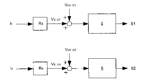
Figure 2 shows a first embodiment of an apparatus for
carrying out the method according to the invention for
operation of a converter circuit. According to the
method, the power semiconductor switches in the
switching cells 3 in the first sub-converter system 1
are controlled by means of a control signal S1, and the
power semiconductor switches in the switching cells 3
in the second sub-converter system 2 are controlled by
means of a further control signal S2. The control
signal S1 for the first sub-converter system 1 is
formed from a reference signal Vref, u. with respect to
the voltage U1 across the first sub-converter system 1.
The further control signal S2 for the second sub-
CA 02730795 2011-02-03
- 10 -
converter system 2 is formed from a reference signal
Vref, U2 with respect to the voltage U2 across the second
sub-converter system 2. As shown in Figure 2, the
control signal S1 is now additionally formed from a
damping signal Vd,ul with respect to the first sub-
converter system 1, wherein the damping signal Vd, U1 is
formed from a measured current ii through the first
sub-converter system 1, and from a predeterminable
resistance value Rd. The damping signal Vd, U1 is formed
in accordance with the following formula:
Vd, ui = i1-Rd [11
The further control signal S2, as shown in Figure 2, is
additionally formed from a damping signal Vd,U2 with
respect to the second sub-converter system 2, wherein
the damping signal Vd, U2 is formed from a measured
current i2 through the second sub-converter system 2
and from the predeterminable resistance value Rd. The
damping signal Vd, U2 is formed in accordance with the
following formula:
Vd, U2 = i 2 = Rd [21
The effect of the respective damping signal Vd, ui, Vd, U2
corresponds to a voltage drop across a non-reactive
resistance in the associated sub-converter system 1, 2,
and therefore damps the currents il, i2 through the
respectively associated sub-converter system 1, 2 in a
desired manner.
As shown in Figure 2, the sum is formed from the
damping signal Vd,ul with respect to the first sub-
converter system 1 and from the reference signal Vref, Ui
with respect to the voltage Ui across the first sub-
converter system 1 and is passed to a modulator 5 which
generates the control signal S1 therefrom. Furthermore,
as shown in Figure 2, the sum is formed from the
damping signal Vd, U2 with respect to the second sub-
CA 02730795 2011-02-03
- 11 -
converter system 2 and from the reference signal Vref, U2
with respect to the voltage U2 across the second sub-
converter system 2, and is passed to a modulator 6,
which generates the further control signal S2
therefrom. All modulators, such as pulse-width
modulators, modulators based on carrier methods, space-
vector modulators or modulators with a hysteresis
characteristic may be used as modulators 5, 6 in
Figure 2, or else in the embodiments as shown in
Figure 3 to Figure 5.
The damping signal Vd, U1 with respect to the first sub-
converter system 1 according to a second embodiment of
an apparatus for carrying out the method according to
the invention as shown in Figure 3 for operation of a
converter circuit is preferably additionally formed
from a predeterminable reference current Iref, ui through
the first sub-converter system 1. The damping signal
Vd,Ui is formed in accordance with the following
formula:
Vd, Ul = (i1 - Iref, u) =Rd [3]
As shown in Figure 3, the damping signal Vd, U2 with
respect to the second sub-converter system 2 is
additionally formed from a predeterminable reference
current Iref, U2 through the second sub-converter system
2. The damping signal Vd, U2 is formed in accordance with
the following formula:
Vd, U2 = (il - Iref, U2) -Rd [4]
The control signal S1 and the further control signal S2
are then formed as shown in Figure 3, in a
corresponding manner to that in Figure 2.
The presetting of a reference current Iref, ui, Iref, U2 for
the formation of the respective damping signal Vd,U1,
Vd, U2 advantageously makes it possible for specific
CA 02730795 2011-02-03
- 12 -
oscillation components of the currents i1, i2 through
the respective sub-converter system to be deliberately
damped.
Figure 4 shows a third embodiment of an apparatus for
carrying out the method according to the invention for
operation of a converter circuit, illustrating an
alternative to the embodiments shown in Figure 2 and
Figure 3. As shown in Figure 4, the control signal Si
for the first sub-converter system 1 is formed from a
reference signal Vref, uzi, which is produced in a central
calculation unit 7, with respect to the associated
switching cell 3 in the first sub-converter system 1. A
local calculation unit 8 is then provided for each
switching cell 3 in the first sub-converter system 1,
wherein the reference signal Vref, uzi with respect to the
associated switching cell 3 in the first sub-converter
system 1 is transmitted to the local calculation units
8 for the switching cells 3 in the first sub-converter
system 1. Furthermore, the control signal S1 is
additionally formed in each local calculation unit 8
for the switching cells 3 in the first sub-converter
system 1 from a damping signal Vd,ZI with respect to the
associated switching cell 3 in the first sub-converter
system 1, wherein the damping signal Vd,Z1 is formed
from a measured current ii through the associated
switching cell 3 in the first sub-converter system 1
and from a predeterminable resistance value Rd. The
damping signal Vd,Z1 is formed in accordance with the
following formula:
Vd, Z1 = it = Rd [51
As shown in Figure 4, the further control signal S2 for
the second sub-converter system 2 is formed from a
reference signal Vref, uz2, which is produced in the
central calculation unit 7, with respect to the
associated switching cell 3 in the second sub-converter
system 2. A local calculation unit 9 is provided for
CA 02730795 2011-02-03
- 13 -
each switching cell 3 in the second sub-converter
system 2, wherein the reference signal Vref, UZ2 with
respect to the associated switching cell 3 in the
second sub-converter system 2 is transmitted to the
local calculation units 9 for the switching cells 3 in
the second sub-converter system 2. Furthermore, the
further control signal S2 is additionally formed in
each local calculation unit 9 for the switching cells 3
in the second sub-converter system 2 from a damping
signal Vd, Z2 with respect to the associated switching
cell 3 in the second sub-converter system 2, wherein
the damping signal Vd, Z2 is formed from a measured
current i2 through the associated switching cell 3 in
the second sub-converter system 2 and from the
predeterminable resistance value Rd. The damping signal
Vd, Z2 is formed in accordance with the following
formula:
Vd, Z2 = il=Rd [6]
The alternative mentioned above and as shown in
Figure 4 results in the currents ii, i2 through the
sub-converter systems 1, 2 advantageously being damped
in the switching cells 3. The effect of the respective
damping signal Vd, Zi, Vd, Z2 corresponds to a voltage drop
across a non-reactive resistance in each switching cell
3, wherein the overall effect corresponds to a series
circuit of non-reactive resistances, by which means the
currents ii, i2 through the respective switching cells
3 in the associated sub-converter systems 1, 2 are
damped in the desired manner. The local measurement of
the currents il, i2 through the switching cells 3
furthermore makes it possible to ensure the redundancy
and therefore the availability of the damping even in
the event of a failure of a current measurement, for
example in a switching cell 3. Furthermore, the local
formation of the control signal S1, S2 avoids the need
for the normal transmission of the control signal S1,
CA 02730795 2011-02-03
- 14 -
S2 to the individual switching cells 3, for example
from a central or superordinate unit.
As shown in Figure 4, the sum is formed from the
damping signal Vd,zl with respect to the associated
switching cell 3 in the first sub-converter system 1
and from the reference signal Vref, uzi with respect to
the associated switching cell 3 in the first sub-
converter system 1, and is passed to a modulator 5,
which generates the control signal Si therefrom.
Furthermore, as shown in Figure 4, the sum is formed
from the damping signal Vd, Z2 with respect to the second
sub-converter system 2 and from the reference signal
Vref, UZ2 with respect to the associated switching cell 3
in the second sub-converter system 2, and is passed to
a modulator 6, which generates the further control
signal S2 therefrom.
The damping signal Vd, zl with respect to the associated
switching cell 3 in the first sub-converter system 1
according to a fourth embodiment of an apparatus for
carrying out the method according to the invention as
shown in Figure 5 for operation of a converter circuit
is preferably additionally formed from a
predeterminable reference current Ireful through the
associated switching cell 3 in the first sub-converter
system 1. The predeterminable reference current Ireful
through the associated switching cell 3 in the first
sub-converter system 1 is transmitted to the local
calculation units 8 for the switching cells 3 in the
first sub-converter system 1. The damping signal Vd,zl
is formed in accordance with the following formula:
Vd, Z1 = (il - Iref, ul) *Rd [71
As shown in Figure 5, the respective damping signal
Vd, Z2 with respect to the associated switching cell 3 in
the second sub-converter system 2 is additionally
formed from a predeterminable reference current Iref, u2
CA 02730795 2011-02-03
- 15 -
through the associated switching cell 3 in the second
sub-converter system 2. The predeterminable reference
current Iref, U2 through the associated switching cell 3
in the second sub-converter system 2 is transmitted to
the local calculation units 9 for the switching cells 3
in the second sub-converter system 1. The damping
signal Vd, Z2 is formed in accordance with the following
formula:
Vd, Z2 = (ii - Iref, U2) Rd [81
The control signal S1 and the further control signal S2
are then formed as shown in Figure 5, in a
corresponding manner to that in Figure 4.
The resistance value Rd is preferably predetermined to
be constant or variable over time.
Figure 6 shows a fifth embodiment of an apparatus for
carrying out the method according to the invention for
operation of a converter circuit, which represents an
alternative to the embodiments shown in Figure 2,
Figure 3, Figure 4 and Figure 5. As shown in Figure 6,
the control signal S1 for the first sub-converter
system 1 is formed from a damping reference signal
Vref,d Ul, which is produced in a central calculation unit
7, with respect to the voltage U1 across the first sub-
converter system 1, wherein the damping reference
signal Vref,d u1 with respect to the voltage Ul across the
first sub-converter system 1 is formed from a
predeterminable reference current lref,Ul through the
first sub-converter system 1, from a predeterminable
resistance value Rda and from a reference signal Vref, U1
with respect to the voltage U1 across the first sub-
converter system 1. The damping signal Vref,d Ul is formed
in accordance with the following formula:
Vref,d U1 = Vref, U1 = (1-ref, Ul"Rda) 191
CA 02730795 2011-02-03
- 16 -
Furthermore, a local calculation unit 8 is provided for
each switching cell 3 in the first sub-converter system
1 as shown in Figure 6, wherein the damping reference
signal Vref,d ul with respect to the voltage Ul across the
first sub-converter system 1 is transmitted to the
local calculation units 8 for the switching cells 3 in
the first sub-converter system 1. The control signal Si
is additionally formed in each of the local calculation
units 8 for the switching cells 3 in the first sub-
converter system 1 from a damping signal Vd,zl with
respect to the associated switching cell 3 in the first
sub-converter system 1, wherein the damping signal Vd,Z1
is formed from a measured current it through the
associated switching cell 3 in the first sub-converter
system 1 and from a predeterminable further resistance
value Rdb. The damping signal Vd, zl is formed in
accordance with the following formula:
Vd, Z1 = i1 -Rdb [10]
As shown in Figure 6, the sum is formed from the
damping signal Vd,Z1 with respect to the associated
switching cell 3 in the first sub-converter system 1
and from the damping reference signal Vref,d ul with
respect to the voltage U1 across the first sub-
converter system 1, and is passed to a modulator 5,
which generates the control signal S1 therefrom.
As shown in Figure 6, the further control signal S2 for
the second sub-converter system 2 is formed from a
damping reference signal Vref,d u2, which is produced in
the central calculation unit 9, with respect to the
voltage U2 across the second sub-converter system 2,
wherein the damping reference signal Vref,d u2 with
respect to the voltage U2 across the second sub-
converter system 2 is formed from a predeterminable
reference current -ref, u2 through the second sub-
converter system 2, from the predeterminable resistance
value Rda and from a reference signal Vref, u2 with
CA 02730795 2011-02-03
- 17 -
respect to the voltage U2 across the second sub-
converter system 2. The damping signal Vref,d U2 is formed
in accordance with the following formula:
Vref,d U2 = Vref, U2 - (lref, U2'Rda) [11]
As shown in Figure 6, a local calculation unit 9 is
provided for each switching cell 3 in the second sub-
converter system 2, and the damping reference signal
Vref,d U2 with respect to the voltage U2 across the second
sub-converter system 2 is transmitted to the local
calculation units 9 for the switching cells 3 in the
second sub-converter system 2. The further control
signal S2 is additionally formed, as shown in Figure 6,
in each of the local calculation units 9 for the
switching cells 3 in the second sub-converter system 2
from a damping signal Vd, Z2 with respect to the
associated switching cell 3 in the second sub-converter
system 2, wherein the damping signal Vd, Z2 is formed
from a measured current i2 through the associated
switching cell 3 in the second sub-converter system 2
and from the predeterminable further resistance value
Rdb. The damping signal Vd, Z2 is formed in accordance
with the following formula:
Vd, Z2 = i2=Rdb [12]
As shown in Figure 6, the sum is formed from the
damping signal Vd,Z2 with respect to the associated
switching cell 3 in the second sub-converter system 2
and from the damping reference signal Vref,d U2 with
respect to the voltage U2 across the second sub-
converter system 2, and is passed to a modulator 6,
which then generates the further control signal S2
therefrom.
The alternative of the invention as shown in Figure 6
also makes it possible to selectively damp specific
oscillation components in the currents il, i2 through
CA 02730795 2011-02-03
- 18 -
the switching cells 3 in the associated sub-converter
system 1, 2. Furthermore, the respective reference
current 1ref, U1, 1ref, u2 is advantageously not transmitted
to the local calculation units 8, 9. The resistance
value Rda is preferably chosen such that it increases
the contribution of the respective reference current
lref, U1, lref, U2 with respect to the damping signal Vd, 21,
Vd,Z2 which is formed in the respectively associated
local calculation unit 8, 9.
The resistance value Rda and the further resistance
value Rdb are preferably predetermined to be constant or
variable over time.
In an entirely general form, it is also feasible for
the respective damping signal Vd, U1, Vd, U2, Vd, 211 Vd, Z2
to be predetermined in accordance with a general
function, in which case a function such as this can
then, for example, contain a constant component, a
component which varies over time, an integral
component, a differential component, a reference
component and a previous value of the respective
damping signal, or a combination of the options stated
above.
CA 02730795 2011-02-03
- 19 -
List of reference symbols
1 First sub-converter system
2 Second sub-converter system
3 Switching cell
4 Phase module
5, 6 Modulator
7 Central calculation unit
8, 9 Local calculation unit