Note : Les descriptions sont présentées dans la langue officielle dans laquelle elles ont été soumises.
CA 02731894 2011-02-16
35717-CA-PAT -1-
POWER DISTRIBUTION NETWORK BASED ON MULTIPLE CHARGE STORAGE
COMPONENTS
[0001] The present application relates generally to power distribution
networks
and, more specifically, to a power distribution network based on multiple
charge
storage components.
[0002] In a power distribution network with a power pack having a charge
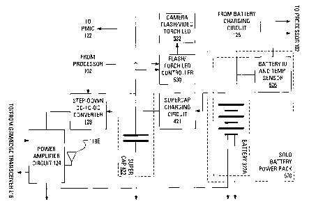
storage component (such as a battery), ripple in the power supply voltage may
result
from pulsed high-current draw by, for example, a radio frequency power
amplifier
circuit. Propagation of the ripple to other components relying on the power
distribution network may cause undesirable effects. For an audio circuit, for
example,
the ripple may cause an audible buzz. Additionally, certain arrangements of
the
power pack relative to the power amplifier circuit may allow for generation of
significant electromagnetic interference.
GENERAL
[0003] By dividing a single power supply into multiple charge storage
components, power supply ripple may be reduced by buffering, at a secondary
charge storage component, a pulsed high current that the power amplifier
circuit may
draw from the primary power supply.
[0004] In accordance with one embodiment, there is provided a power
distribution network. The power distribution network includes a primary
charging
circuit, a first charge storage component having a first terminal connected to
the
charging circuit and a second terminal connected to a power supply common
voltage, a secondary charging circuit, a second charge storage component
having a
first terminal connected to the secondary charging circuit and a second
terminal
connected to the power supply common voltage and a converter having an input
terminal and an output terminal, the input terminal receiving an input voltage
from the
first terminal of the second charge storage component, and the output terminal
supplying an output voltage with a magnitude altered relative to the input
voltage.
CA 02731894 2011-02-16
35717-CA-PAT -2-
[0005] Other aspects and features of the present invention will become
apparent
to those of ordinary skill in the art upon review of the following description
of specific
embodiments of the invention in conjunction with the accompanying figures.
BRIEF DESCRIPTION OF THE DRAWINGS
[0006] Reference will now be made to the drawings, which show by way of
example, embodiments of the present disclosure, and in which:
[0007] FIG. 1 illustrates a power distribution network with a power amplifier
circuit and a single battery;
[0008] FIG. 2 schematically illustrates the power amplifier circuit of the
power
distribution network of FIG. 1, as supplied with power by a single battery;
[0009] FIG. 3 schematically illustrates a power amplifier circuit for use in a
power
distribution network, as supplied with power by multiple batteries;
[0010] FIG. 4 illustrates a power amplifier circuit for use in a power
distribution
network, where the power amplifier circuit includes a power pack enclosing a
supercapacitor and a battery; and
[0011] FIG. 5 illustrates a power amplifier circuit for use in a power
distribution
network having additional components, where the power amplifier circuit
includes a
supercapacitor and a battery, where the supercapacitor is arranged to supply
power
to the additional components.
DESCRIPTION OF THE PREFERRED EMBODIMENTS
[0012] FIG. 1 illustrates a power distribution network 100 with a power
amplifier
circuit 124 and a power pack 120. The power pack 120 includes at least one
charge
storage component. As will be discussed below, the charge storage component
may
be any component that stores electrical charge, such as a chemical power cell
or a
supercapacitor. The power distribution network 100 is arranged for use in a
mobile
communication device. The mobile communication device includes a processor 102
for controlling the overall operation of the mobile communication device, or
for
controlling selected operations of the mobile communication device. Components
of
CA 02731894 2011-02-16
35717-CA-PAT -3-
the mobile communication device include a housing (not shown) and multiple
user
interface components 104. The user interface components 104 may include an
input
device (e.g., a keyboard having a plurality of keys, a button, a trackball or
touchpad)
and an output device (e.g., a display), which may comprise a full graphic, or
full
color, Liquid Crystal Display (LCD). In some embodiments, the display may
comprise
a touchscreen display. In such embodiments, the keyboard may comprise a
virtual
keyboard. Other types of output devices may alternatively be utilized. The
processor
102 controls the operation of the display, in part, responsive to actuation of
the keys
on the keyboard by a user of the mobile communication device.
[0013] Components of the mobile communication device may also include an
audio circuit 106, which may control presentation, to the user, of an audio
alert (a
ring tone), audio received in a telephone call and audio based on a digital
music file
saved in device memory (not shown).
[0014] Components of the mobile communication device may also include a
receiver 108 for use with the known global positioning system (GPS). The GPS
receiver 108 is illustrated as being communicatively connected to a GPS
receiver
= antenna 118A.
[0015] Components of the mobile communication device may also include a
transceiver 110 for use in a short-range communications subsystem that enables
communication between the mobile communication device and other proximate
systems or devices, which need not necessarily be similar devices. For
example, the
short-range communications subsystem may include an infrared device and
associated circuits and components, or a BluetoothTM communication module to
provide for communication with similarly-enabled systems and devices. The
Bluetooth transceiver 110 is illustrated as being communicatively connected to
a
Bluetooth transceiver antenna 11 8B.
[0016] Components of the mobile communication device may also include a
transceiver 112 for use in a wireless local area networking communication
subsystem. A set of standards has been established by the Institute of
Electrical and
Electronics Engineers (IEEE) and is known as IEEE 802.11 standards. Products
may
be certified by the known Wi-Fi Alliance for adherence to the IEEE 802.11
standards.
CA 02731894 2011-02-16
35717-CA-PAT -4-
The Wi-Fi transceiver 112 is illustrated as being communicatively connected to
a Wi-
Fi transceiver antenna 11 8C.
[0017] Components of the mobile communication device may also include a
transceiver 114 for use in a first wireless telecommunication subsystem. The
first
wireless telecommunication subsystem may be based on the known Wideband Code
Division Multiple Access (W-CDMA) standard. The W-CDMA transceiver 114 is
illustrated as being communicatively connected to a W-CDMA transceiver antenna
118D.
[0018] Components of the mobile communication device may also include a
transceiver 116 for use in a second wireless telecommunication subsystem. The
second wireless telecommunication subsystem may be based on the known Global
System for Mobile communications (GSM) and Enhanced Data rates for GSM
Evolution (EDGE) standards. The GSM/EDGE transceiver 116 is illustrated as
being
communicatively connected, through the power amplifier circuit 124, to a
GSM/EDGE transceiver antenna 11 8E.
[0019] The processor 102, the user interfaces 104, the audio circuit 106, the
GPS receiver 108, the Bluetooth transceiver 110, the Wi-Fi transceiver 112,
the W-
CDMA transceiver 114 and the GSM/EDGE transceiver 116 all maintain a
connection to a power management integrated circuit (PMIC) 122.
[0020] The PMIC 122 and the power amplifier circuit 124 maintain a connection
to the power pack 120. The power pack 120, through a first terminal 132A,
maintains
a connection to the PMIC 122 and to a battery charging circuit 126. The power
pack
120, through a second terminal 134A, maintains a connection to a power supply
reference voltage in common with components of the power amplifier circuit
124.
Another pair of terminals includes a third terminal 1328 connecting the power
pack
120, through a step-down direct current to direct current (DC-to-DC) converter
128,
to the power amplifier circuit 124 and a fourth terminal 134B connecting the
power
pack 120 to the power supply reference voltage.
[0021] The step-down DC-to-DC converter 128 receives, at an input terminal,
the
voltage available at the third terminal 132A of the power pack 120, converts
the
CA 02731894 2011-02-16
35717-CA-PAT -5-
voltage received at the input terminal to a lower voltage and makes the lower
voltage
available, at an output terminal, to the power amplifier circuit 124.
[0022] The power pack 120 may, for example, house a Li-Ion battery with an
operational range of from 4.2V to 3.2V. The concepts described herein are not
limited, however, to any particular form of energy storage or battery
chemistry.
[0023] Components of the power amplifier circuit 124 of FIG. 1 are illustrated
in
FIG. 2. The power amplifier circuit 124 includes (but is not necessarily
limited to) a
power amplifier 202 that connects to an output of the GSM/EDGE transceiver 116
and to an input to a low pass filter 204. A switch 206 connects, in one state,
the
output of the low pass filter 204 to an antenna matching circuit 208, which
connects
to the GSM/EDGE transceiver antenna 118E. In another state, switch 206
connects
the output of the antenna matching circuit 208 to an input of a band pass
filter 210.
The output of the band pass filter 210 connects to an input of the GSM/EDGE
transceiver 116.
[0024] The power amplifier 202 is illustrated as comprising multiple stages
(not
individually referenced) with each stage receiving a power supply voltage from
a first
terminal 212A of the power pack 120. Similarly, each stage shares power supply
reference voltage with a second terminal 214A of the power pack 120.
[0025] In operation, the GSM/EDGE transceiver 116 may cause the power
amplifier 202 to be operated in a so-called "pulse mode". The pulse mode of
power
amplifier operation is known to cause variation in the power supply voltage
provided
at the first terminal 212 of the power pack 120. The variation, or ripple, in
the power
supply voltage may be as much as 400mV peak-to-peak due to high pulsed
current.
Unfortunately, the ripple may propagate from the power pack 120, to the PMIC
122,
to the rest of the components. For the audio circuit 106, the ripple may cause
an
audible buzz (for GSM-based communication devices, many have experienced a
buzz at 217Hz), elimination of which has been perceived as difficult and
costly.
[0026] The efficiency of the power amplifier 202 is generally maintained by a
stable supply voltage. Unfortunately, in the case wherein the power pack 120
houses
only a single charge storage component, during use, the power supply voltage
provided at the third terminal 1328 of the power pack 120 can change, as the
charge
CA 02731894 2011-02-16
35717-CA-PAT -6-
on the charge storage component is diminished, from 4.2V (fully charged) to as
low
as 3.2V (needing recharge). Indeed, when the charge on the charge storage
component has been reduced and the power supply voltage provided at the third
terminal 132B of the power pack 120 is correspondingly reduced, the power
amplifier
202 may be forced into an undesired saturation mode. When the power amplifier
202 is operating in saturation mode, the power level of the radio frequency
(RF)
signal output to the GSM/EDGE transceiver antenna 118E is reduced relative to
a
preferred power level. Additionally, it may be considered that operation of
the power
amplifier 202 in saturation mode compromises the output spectrum.
[0027] Furthermore, when designing the power amplifier 202 to account for
operation in wide range supply voltages, design sacrifices or accommodations
are
required to be made. For example, such design sacrifices may include the
addition of
circuits designed to control the behavior of the power amplifier 202 under
reduced
supply voltage. One such circuit is known as an anti-saturation loop. Such
additional
circuits may be considered to increase the complexity and cost of the power
amplifier
202.
[0028] A power amplifier current loop may be defined as being formed through
the power pack 120 and the power amplifier 202. With the relatively large area
of the
loop, it may be shown that the pulse mode of power amplifier operation causes
measurable magnetic radiation to be emitted. This emission may be shown to
interfere with other circuits, such as the circuits found in hearing aids,
especially
among the circuits found in hearing aids that utilize a T-magnetic coil (or T-
coil) to
pick up an audio signal. The emission of magnetic radiation from the power
amplifier
current loop can also be problematic when the radiation couples to various
transducers and other components within the enclosure of the mobile
communication
device to which the power distribution network 100 provides power.
[0029] It may be shown that Radio Frequency (RF) interference signals (any
unwanted signals) that are present at the power amplifier 202 during
transmission
may be coupled to other circuits 104, 106, 108, 110, 112, 114, 116, 122, 126
via the
power supply lines. If the interference signals become coupled to the battery
housed
by the power pack 120, for example, it can be shown that those interference
signals
may be radiated by the battery due to the charge storage component structure.
The
CA 02731894 2011-02-16
35717-CA-PAT -7-
charge storage component structure may, for example, involve the third
terminal
132B (i.e., the positive contact) of the power pack 120 being connected to the
mobile
communication device housing. In such a case, it may be shown that the mobile
communication device housing may behave like an antenna.
[0030] In overview, by dividing the power supply into more than one charge
storage components, power supply ripple may be reduced by buffering, at a
secondary power supply, a pulsed high current that the power amplifier circuit
may
draw from the primary power supply.
[0031] When the designer of the circuit supplying power to the power amplifier
202 mandates, to a vendor designing the power amplifier 202, that the power
amplifier 202 has to handle a wide supply voltage range, the flexibility of
the vendor
to design the power amplifier 202 for improved linearity and higher efficiency
is
reduced. Conveniently, when the circuit supplying power to the power amplifier
202
is designed as proposed herein, vendors will have more freedom and flexibility
to
design the power amplifier 202.
[0032] A first solution to the above set of problems involves providing
multiple
batteries in the power pack 120 rather than a single battery. For example,
FIG. 3
illustrates the power amplifier circuit 124 as supplied with power by multiple
charge
storage components. The multiple charge storage components are provided in a
dual battery power pack 320.
[0033] The dual battery power pack 320 includes a first battery 322A and a
second battery 322B. The first battery 322A has a first terminal connected to
the
battery charging circuit 126 and a second terminal connected to a common
supply
voltage for the power distribution network. A second terminal of the second
battery
322B is also connected to the common supply voltage for the power distribution
network. A first terminal of the second battery 322B and the first terminal of
the first
battery 322A are connected to, and interposed by, a dual-battery charging
circuit
321. While the battery charging circuit 126 may be considered to be a
"primary"
charging circuit, the dual-battery charging circuit 321 may be considered to
be a
"secondary" charging circuit.
CA 02731894 2011-02-16
35717-CA-PAT -8-
[0034] The step-down DC-to-DC converter 128, familiar from FIGS. 1 and 2,
converts the voltage available at the first terminal of the second battery
322B to a
lower voltage and makes the lower voltage available to the power amplifier
circuit
124. The power amplifier circuit 124 of FIG. 3 is arranged to receive a signal
from the
GSM/EDGE transceiver 116 for transmission on the GSM/EDGE transceiver
antenna 118E. Additionally, the power amplifier circuit 124 of FIG. 3 is
arranged to
receive a signal from the GSM/EDGE transceiver antenna 11 8E and transmit the
received signal to the GSM/EDGE transceiver 116.
[0035] The dual battery power pack 320 includes a battery identifier and
temperature sensor 326. The battery identifier and temperature sensor 326
connects
to the processor 102 (FIG. 1). The battery identifier portion is adapted to
output an
identification of the dual battery power pack 320. The temperature sensor
portion is
adapted to sense a temperature within the dual battery power pack 320 and
provide
an output signal indicative of the temperature to the processor 102.
[0036] Conveniently, in operation, the dual-battery charging circuit 321 can
act to
continuously charge the second battery 322B, thereby maintaining a more
consistent
charge on the second battery 322B than would be possible with a single-battery
power pack. Consequently, the power amplifier circuit 124 of FIG. 3 may be
designed to take advantage of a consistent voltage at the output of the step-
down
DC-to-DC converter 128 in a manner unavailable to the designer of the power
amplifier circuit 124 of FIG. 1. By continuously charging the second battery
322B, the
Equivalent Series Resistance (ESR) of the second battery 322B may be
maintained
at a magnitude that is consistently lower than the ESR of the first battery
322A.
Consequently, a majority of the high pulsed current drawn by the power
amplifier
circuit 124 will pass though the second battery 322B.
[0037] In the case wherein the power pack has only a single charge storage
component (such as a Li-Ion battery), the power amplifier circuit 124 may be
designed to handle an operational range of supply voltage that extends from
4.2V to
3.2V. As a result of using a power pack with multiple charge storage
components, as
disclosed herein, the range of the supply voltage may be tightened to, for
example, a
range that extends from 3.6V to 3.5V. By tightening the range of the supply
voltage
that the power amplifier circuit 124 is to be able to handle, the power
amplifier
CA 02731894 2011-02-16
35717-CA-PAT -9-
designer can improve the performance of the power amplifier circuit 124. Such
performance improvement may include increased output power, increased
efficiency
and improved linearity.
[0038] The second battery 322B may be seen to buffer a pulsed high current
draw from the first battery 322A and, as a consequence, the audible buzz, due
to
propagation of the power supply ripple to the audio circuit 106, may be
significantly
reduced.
[0039] Notably, the concepts described in the present application do not
necessarily exclude other approaches to reduction of the effects of ripple.
Indeed,
advantageously, the approaches described in herein may work non-exclusively
with
other approaches to reduction of the effects of ripple.
[0040] A second solution to the above set of problems involves replacement of
the second battery 322B in the dual battery power pack 320 of FIG. 3 with an
alternative charge storage component in the form of a supercapacitor 422,
thereby
completing contents of a hybrid battery power pack 420 (see FIG. 4).
[0041] In general, a supercapacitor resembles a regular capacitor with the
exception that a supercapacitor offers very high capacitance in a small
package.
Energy storage is accomplished by means of static charge rather than being
accomplished by means of an electro-chemical process, such as in the manner of
a
conventional chemical battery. In common with a regular capacitor, a
supercapacitor
has a positive plate and a negative plate. By applying a voltage differential
to the
positive and negative plates, a charge may be stored in the supercapacitor.
Whereas
a regular capacitor typically includes conductive foils and a dry separator,
the
supercapacitor typically includes special electrodes and an electrolyte.
[0042] The known Part No. EDLC152344-551-2F-30 by TDK of Nihombashi,
Chuo, Tokyo, Japan is an example of a component that may be used for the
supercapacitor 422. Specifications of this example component include:
dimensions
23x44x1.5 mm; rated voltage - 4.2V continuous bias, 5.7V intermittent bias;
and
nominal capacitance 550mF. The concepts described herein are not limited,
however, to any particular supercapacitor, or any particular capacitance, or
any
particular structure for charge storage or charge separation.
CA 02731894 2011-02-16
35717-CA-PAT _10-
[0043] In common with the dual battery power pack 320, the first battery 322A
of
hybrid battery power pack 420 has a first terminal connected to the battery
charging
circuit 126 and a second terminal connected to a common supply voltage for the
power distribution network. A second terminal of the supercapacitor 422 is
also
connected to the common supply voltage for the power distribution network. A
first
terminal of the supercapacitor 422 and the first terminal of the first battery
322A are
connected to, and interposed by, a supercapacitor charging circuit 421. The
step-
down DC-to-DC converter 128 converts the voltage available at the first
terminal of
the supercapacitor 422 to a lower voltage and makes the lower voltage
available to
the power amplifier circuit 124.
[0044] As will be clear to one skilled in the art, the power distribution
network 100
can be designed with more than one supercapacitor if there is more than one
high
current load.
[0045] The hybrid battery power pack 420 includes a battery identifier and
temperature sensor 426. The battery identifier and temperature sensor 426
connects
to the processor 102 (FIG. 1) to provide battery identity and information
regarding
the temperature of the hybrid battery power pack 420.
[0046] In a manner consistent with the dual-battery charging circuit 321, the
supercapacitor charging circuit 421 can act to maintain a consistent charge on
the
supercapacitor 422, thereby distinguishing the hybrid battery power pack 420
from a
single-battery power pack, for which a consistent charge is desired but, as
has been
discussed hereinbefore, is difficult to achieve.
[0047] The supercapacitor charging circuit 421, and the dual-battery charging
circuit 321, may be implemented as a standard switched power supply, which can
be
a step-up converter or a step-down converter with a predetermined charging
current.
However, it should be clear that the present disclosure is not dependent on a
particular implementation of charging circuit.
[0048] In various embodiments, the step-down DC-to-DC converter 128 may be
short-circuited, so that the second battery 322B in the dual battery power
pack 320
of FIG. 3 or the supercapacitor 422 in the hybrid battery power pack 420 of
FIG. 4 is
directly connected to the power amplifier circuit 124. In such an embodiment,
the
CA 02731894 2011-02-16
35717-CA-PAT _11-
charging circuit, e.g., the dual-battery charging circuit 321 in FIG. 3 or the
supercapacitor charging circuit 421 in FIG. 4, serves as both a charging
circuit and a
voltage regulating circuit. The second battery 322B or the supercapacitor 422
in
these alternative embodiments retain their use as providers of the majority of
the
instant power required from the power amplifier circuit 124 during a pulsed
high
current draw.
[0049] In a further alternative embodiment, the charging circuit, e.g., the
dual-
battery charging circuit 321 in FIG. 3 or the supercapacitor charging circuit
421 in
FIG. 4, may be short circuited, so that the second battery 322B or the
supercapacitor
422 is directly connected to the first battery 322A, while the step-down DC-to-
DC
converter 128 is used to regulate the battery output voltage to a fixed supply
voltage
to the power amplifier circuit 124. The second battery 322B or the
supercapacitor
422 in these alternative embodiments retain their use as providers of the
majority of
the instant power required from the power amplifier circuit 124 during a
pulsed high
current draw.
[0050] In a manner consistent with the dual battery power pack 320 having an
ESR that is lower than the ESR of the single battery 122, it may be shown that
the
ESR of the combination of the step-down DC-to-DC converter 128 and the hybrid
battery power pack 420 also has a lower ESR than a hypothetical single-battery
power pack. Experimentation has shown that the ESR of the hypothetical single-
battery power pack may be in the order of 150 mU, while the ESR of the
combination
of the step-down DC-to-DC converter 128 and the hybrid battery power pack 420
may be in the order of only 30 mfg.
[0051] A third solution to the above set of problems involves rearrangement of
the components of the hybrid battery power pack 420 of FIG. 4 such that only
the
first battery 322A remains inside a battery power pack, thereby leading to the
naming
of a solo battery power pack 520.
[0052] In common with the dual battery power pack 320 and the hybrid battery
power pack 420, the first battery 322A of a solo battery power pack 520 has a
first
terminal connected to the battery charging circuit 126 and a second terminal
connected to a common supply voltage for the power distribution network. A
second
CA 02731894 2011-02-16
35717-CA-PAT -12-
terminal of the supercapacitor 422, which is external to the solo battery
power pack
520, is also connected to the common supply voltage for the power distribution
network. Just as in the circuit of FIG. 4, a first terminal of the
supercapacitor 422 and
the first terminal of the first battery 322A are connected to, and interposed
by, the
supercapacitor charging circuit 421. The step-down DC-to-DC converter 128
converts the voltage available at the first terminal of the supercapacitor 422
to a
lower voltage and makes the lower voltage available to the power amplifier
circuit
124.
[0053] The solo battery power pack 520 includes a battery identifier and
temperature sensor 526. The battery identifier and temperature sensor 526
connects
to the processor 102 (FIG. 1) to provide battery identity and information
regarding
the temperature of the solo battery power pack 520.
[0054] The circuit of FIG. 5 includes additional components that may be found
in
mobile communication devices. The additional components include a Light
Emitting
Diode (LED) 532 for use as a flash when using the mobile communication device
to
capture a still photograph. The LED 532 may also be used as a torch to provide
light
when the mobile communication device is used to capture video. Associated
with,
and connected to, the LED 532 is a controller 530. The controller 530 receives
power
from the first terminal of the supercapacitor 422. Additionally, the
controller 530
receives instructions from the processor 102 (FIG. 1).
[0055] It has been discussed hereinbefore that the pulse mode of power
amplifier
operation is known to cause a ripple in the power supply voltage provided at a
battery and that the ripple may be shown to adversely affect operation of
other
circuits. It may also be shown that other circuits in a typical mobile
communication
device can cause a ripple in the power supply voltage. An example of such a
ripple-
causing circuit is the combination of the LED 532 and the controller 530 in
FIG. 5.
[0056] In a typical mobile communication device, the power amplifier circuit
124
and the LED 532 may not be operated at the same time due to high pulsed power
consumption and the resultant voltage ripples propagating to other circuits.
It can be
shown that use of the supercapacitor 422, with the step-down DC-to-DC
converter
128 and the supercapacitor charging circuit 421, will allow simultaneous
operation of
CA 02731894 2011-02-16
35717-CA-PAT _13-
the power amplifier circuit 124 and the LED 532, without causing significant
power
supply voltage ripples to propagate to other circuits. Indeed, testing has
shown that
power supply voltage ripples may be reduced from 400 mV peak-to-peak to less
than
200 mV peak-to-peak.
[0057] Conveniently, and in contrast to the power distribution networks
represented by the circuits of FIGS. 1, 2, 3 and 4, the circuit of FIG. 5
makes
available continued operation of the mobile communication device even in the
absence of the solo battery power pack 520. Accordingly, the mobile
communication
device may, for example, continue to participate in a cellular telephone call
or
continue to play a digital music file, even as a previously installed solo
battery power
pack is exchanged for a replacement solo battery power pack.
[0058] As discussed hereinbefore, efficiency of the power amplifier circuit
124
may be improved through designing the power amplifier circuit 124 for a
tightly
regulated supply voltage from the step-down DC-to-DC converter 128. Such
improved efficiency during operation may be further improved by dynamically
setting
the output of the step-down DC-to-DC converter 128 to the power amplifier
circuit
124 based on a desired output power level. To this end, the step-down DC-to-DC
converter 128 may receive instructions from the processor 102 (FIG. 1).
Notably, the
instructions may be of any kind, including instructions in the form of
modulated
pulses.
[0059] It has been discussed hereinbefore that when the charge on a single
battery housed by the power pack 120 has been reduced and the power supply
voltage provided at the third terminal 132B (FIG. 2) of the power pack 120 is
correspondingly reduced, the power amplifier 202 may be forced into a mode of
operation known as "saturation". When the power amplifier 202 is operating in
saturation mode, the power level of the radio frequency (RF) signal output to
the
GSM/EDGE transceiver antenna 118E is reduced relative to a preferred power
level
in order to revert the power amplifier 202 out of the saturation. By
appropriately
setting the output of the step-down DC-to-DC converter 128 to the power
amplifier
circuit 124, the power amplifier circuit 124 may be prevented from entering
into
saturation mode.
CA 02731894 2011-02-16
35717-CA-PAT -14-
[0060] The power amplifier current loop defined in FIG. 2 as being formed
through the power pack 120 and the power amplifier 202 may be defined in FIGS.
4
and 5 as being formed through the step-down DC-to-DC converter 128, the
supercapacitor 422 and the power amplifier 124. The relatively large area of
the
power amplifier current loop defined in FIG. 2 may be reduced by arranging the
step-
down DC-to-DC converter 128 and the supercapacitor 422 to be relatively closer
to
the power amplifier 124. Such an arrangement may be seen to be most feasible
in
the circuit of FIG. 5, wherein the supercapacitor 422 is separate from the
first battery
322A. With a power amplifier current loop defined to have a significantly
reduced
area, it follows that the magnetic emission from the power amplifier current
loop will
have a significantly reduced magnitude, thereby interfering to a lesser degree
with
magnetic susceptible circuits, such as hearing aids, which utilize a T-coil to
pick up
an audio signal.
[0061] RF interference signals have been discussed hereinbefore as being
present at the power amplifier 202 (FIG. 2) during transmission and being
coupled to
other circuits 104, 106, 108, 110, 112, 114, 116, 122, 126 via the power
supply lines.
[0062] The proposed power distribution network may be shown to reduce the
decoupling requirements for all mobile sub circuits.
[0063] Relatively long power supply traces on a printed circuit board (PCB)
used
to implement power distribution networks are known to occupy PCB real estate
and
maintain a relatively high ESR, which may be considered detrimental to the
efficiency of power supplied by the power pack. A further consequence of the
proposed reduced-area power amplifier current loop defined in FIG. 5 is a
reduction
in length of power supply traces, thereby preserving PCB real estate and
reducing
the ESR of the power supply traces, leading to an increase in the efficiency
of the
use of the power from the first battery 322A.
[0064] As should be apparent to a person of ordinary skill in the art, the
alternative charge storage component need not be restricted to the
supercapacitor
422 of FIGS. 4 and 5. Indeed, many other types of capacitors may be suitable.
[0065] Furthermore, as used in the present disclosure, a charging circuit is
described as circuitry that can deliver electrical power from a power supply
(which
CA 02731894 2011-02-16
35717-CA-PAT -15-
may include one or more charge storage components) to a component that
consumes the electrical power. For clarity, the charging circuits and
converters have
been illustrated as distinct elements. In practice, however, charging circuits
and
converters may be combined and may share some circuit elements.
[0066] A person of ordinary skill in the art will appreciate that there exist
a wide
variety of types of converters for use as the converter 128, including
switched
converters. Additionally, although the converter 128 has been disclosed as a
step-
down DC-to-DC converter, there exist applications in which a step-up converter
would be more appropriate. For example, in the case wherein the power
amplifier
circuit 124 is designed for high linearity, the power amplifier circuit 124
may be
designed to use a supply voltage that is higher than the voltage available
from the
installed power pack. In addition to converters that only step-up or step-
down, there
exist converters that both step-up and step-down.
[0067] The above-described embodiments, and variations thereof, may realize
one or more advantages, some of which have been previously mentioned. As noted
above, when the circuit supplying power to the power amplifier 202 (FIG. 2) is
designed as proposed herein, vendors will have more freedom and flexibility to
design the power amplifier circuit 124 and, more specifically, the power
amplifier
202. Additionally, the dual-battery charging circuit 321 (FIG. 3) can act to
continuously charge the second battery 322 B, thereby maintaining a more
consistent
charge on the second battery 322B than would be possible with a single-battery
power pack. By continuously charging the second battery 322B, the ESR of the
second battery 322B may be maintained at a magnitude that is consistently
lower
than the ESR of the first battery 322A so that a majority of the high pulsed
current
drawn by the power amplifier circuit 124 will pass though the second battery
322B.
Further advantageously, the circuit of FIG. 5 makes available continued
operation of
the mobile communication device even in the absence of the solo battery power
pack 520.
[0068] The above-described embodiments of the present application are
intended to be examples only. Alterations, modifications and variations may be
effected to the particular embodiments by those skilled in the art without
departing
from the scope of the application, which is defined by the claims appended
hereto.