Note : Les descriptions sont présentées dans la langue officielle dans laquelle elles ont été soumises.
CA 02734673 2011-02-17
WO 2010/025124 PCT/US2009/054864
TITLE
METHODS OF FABRICATING COMPLEX
TWO-DIMENSIONAL CONDUCTIVE SILICIDES
FIELD
The embodiments disclosed herein relate to the fabrication of complex two-
dimensional
conductive nanostructures, and more particularly to the fabrication of complex
two-dimensional
conductive silicide nanostructures by a chemical vapor deposition method.
BACKGROUND
Simple nanostructures (e.g. nanowires) form complex nanomaterials when
connected by
single crystalline junctions, offering better mechanical strength and superior
charge transport
while preserving unique properties associated with the small dimensions. Great
research interest
has been attracted to study this new class of materials, especially in the
field of electronics and
energy applications. Synthesis of these materials is challenging, necessitated
by the combined
features of low dimensionality and high complexity; the former requires growth
suppressions
whereas the latter demands growth enhancement. To this end, two-dimensional
complex
nanostructures are exceedingly difficult to grow chemically.
SUMMARY
Complex two-dimensional conductive silicide nanostructures and methods of
fabricating
the nanostructures are disclosed.
According to aspects illustrated herein, there is provided a conductive
silicide that
includes a plurality of connected and spaced-apart nanobeams linked together
at an about 90-
degree angle, the plurality of nanobeams forming a two-dimensional
nanostructure having a
mesh-like appearance. In an embodiment, the plurality of nanobeams are
flexible. In an
embodiment, the silicide has an electrical resistivity of approximately 10 p
).cm. In an
embodiment, the conductive silicide can be used in a nanoelectronics device.
In an embodiment,
the conductive silicide can be used in an energy-related device. In an
embodiment, the
1
CA 02734673 2011-02-17
WO 2010/025124 PCT/US2009/054864
conductive silicide can be used in a planar electronic device. In an
embodiment, the conductive
silicide can be used in an optoelectronics device. In an embodiment, the
conductive silicide can
be used in a nanophotonics device.
According to aspects illustrated herein, there is provided a conductive
silicide
nanostructure comprising a plurality of two-dimensional nanonet sheets,
wherein each of the
nanonet sheets include connected and spaced-apart nanobeams linked together at
an about 90-
degree angle. In an embodiment, the plurality of nanonet sheets are stacked
approximately
horizontally. In an embodiment, the plurality of nanonet sheets have an
electrical resistivity of
approximately 10 p) . cm.
According to aspects illustrated herein, there is provided a method of
fabricating a two-
dimensional conductive silicide that includes performing chemical vapor
deposition, wherein one
or more gas or liquid precursor materials carried by a carrier gas stream
react to form a
nanostructure having a mesh-like appearance and including a plurality of
connected and spaced-
apart nanobeams linked together at an about 90-degree angle.
BRIEF DESCRIPTION OF THE DRAWINGS
The presently disclosed embodiments will be further explained with reference
to the
attached drawings, wherein like structures are referred to by like numerals
throughout the several
views. The drawings shown are not necessarily to scale, with emphasis instead
generally being
placed upon illustrating the principles of the presently disclosed
embodiments.
FIG. 1 is a schematic representation of a chemical vapor deposition (CVD)
apparatus
used for an embodiment of a method of fabricating complex two-dimensional (2D)
conductive
silicide nanostructures of the present disclosure.
FIG. 2(A-E) show electron micrographs of a complex 2D conductive titanium
silicide
(TiSi2) nanostructure fabricated according to the methods of the presently
disclosed
embodiments. FIG. 2A is a scanning electron micrograph (SEM) of the 2D
conductive TiSi2
nanostructure. The nanostructure is composed of a plurality of nanonet (NN)
sheets. FIG. 2B is
a transmission electron micrograph (TEM) showing a single NN sheet of the 2D
conductive
TiSi2 nanostructure. Each NN has a complex structure made up of nanobeams that
are linked
2
CA 02734673 2011-02-17
WO 2010/025124 PCT/US2009/054864
together by single crystalline junctions with 90 angles. FIGS. 2(C-E) show a
series of tilted
transmission electron micrographs, and corresponding schematics, of the NN
structure.
FIG. 3(A-C) show a series of tilted scanning electron micrographs (top
images), viewed
at 0 , 15 and 30 , respectively, and corresponding schematics (bottom images)
of a single NN
sheet from a complex 2D conductive titanium silicide (TiSi2) nanostructure
fabricated according
to the methods of the presently disclosed embodiments.
FIG. 4(A-F) show transmission electron micrographs of the complex 2D
conductive
titanium silicide (TiSi2) nanostructure shown in FIG. 2, as well as X-ray
photoelectron
spectroscopy (XPS) peaks of Cl, Si and Ti from the nanostructure. FIG. 4(A-C)
show high-
resolution transmission electron micrographs (HRTEMs) of the single nanobeam
highlighted
from FIG. 2B. The entire nanobeam is single crystalline, including the joint
(FIG. 4A), the
middle (FIG. 4B) and the end (FIG. 4C). To better show the atomic arrangements
in the
HRTEMs, noise reduction by inversed fast Fourier transform (iFFT) was
performed. Figure 4D
shows that noise reduction by inverse Fast Fourier Transform (iFFT) in
selected regions show
the Ti and Si atomic arrangements in excellent agreement with simulated ones
(white-framed
inset). Schematic atomic arrangements viewed from <010> direction is shown in
the top-left
inset of FIG. 4D. XPS peaks of Cl, Si and Ti with peak fittings are plotted in
FIG. 4E. FIG. 4F
shows the NN sheet of FIG. 2C, where the width of the sheet is about 15 nm.
FIG. 5 is an energy dispersive X-ray spectroscopy (EDXRF) spectrum of a
complex 2D
conductive TiSi2 nanostructure fabricated according to the presently disclosed
embodiments. A
ratio of the concentration of Ti:Si is about 1:2.
FIG. 6 show schematic representations of atoms arranged in TiSi2 viewed from
different
perspectives. The difference between C49 (top) and C54 (bottom) lies in the
existence of pure Si
layers perpendicular to the b axis in the atomic structure.
FIG. 7(A-C) show different nanostructures that are obtainable by altering
various process
parameters of the method of the presently disclosed embodiments as well as
Raman spectroscopy
analysis of nanowebs versus nanonet sheets. FIG. 7A is a scanning electron
micrograph showing
TiSi2 nanowebs (NWs) in the form of intersecting nanowires fabricated by
altering the
processing parameters of the method of the presently disclosed embodiments.
FIG. 7B is a
3
CA 02734673 2011-02-17
WO 2010/025124 PCT/US2009/054864
transmission electron micrograph of the TiSi2 NWs. FIG. 7C is a Raman
spectroscopy analysis
showing that TiSi2 NWs are C54 and that TiSi2 NN sheets are C49.
FIG. 8(A-C) show transmission electron micrographs of kinks and melting
phenomenon
observed in a complex 2D conductive TiSi2 nanostructure fabricated according
to the methods of
the presently disclosed embodiments. When a growth front encounters an
existing structure, the
growth front either changes growth direction to form 90 kinks (FIG. 8A) or
melts into the
existing one to form a single crystalline joint, FIG. 8B and 8C.
FIG. 9(A-D) show electrical properties of complex 2D conductive TiSi2
nanostructures
fabricated according to the methods of the presently disclosed embodiments.
FIG. 9(A-B) show
a scanning tunneling microscopy (STM) setup. FIG. 9C shows a tunneling current
versus sample
voltage (I-V) curve for the complex 2D conductive TiSi2 nanostructures. FIG.
9D shows how
annealing by passing a constant current at a large bias helps form Ohmic
contacts between the
STM tip and the TiSi2 nanostructures.
While the above-identified drawings set forth presently disclosed embodiments,
other
embodiments are also contemplated, as noted in the discussion. This disclosure
presents
illustrative embodiments by way of representation and not limitation. Numerous
other
modifications and embodiments can be devised by those skilled in the art which
fall within the
scope and spirit of the principles of the presently disclosed embodiments.
DETAILED DESCRIPTION
Silicides are highly conductive materials formed by alloying silicon with
selected metals.
They are commonly used in Si integrated circuits to form ohmic contacts. The
most frequently
used silicides in advanced integrated circuits are silicides of titanium
(TiSiz), cobalt (CoSi2), and
nickel (NiSi). Titanium silicide (TiSi2) is an excellent electronic material
and is one of the most
conductive silicides (resistivity of about 10 micro-ohm-centimeters (ii
).cm)). TiSi2 has recently
been demonstrated to behave as a good photocatalyst to split water by
absorbing visible lights, a
promising approach toward solar H2 as clean energy carriers. Better charge
transport offered by
complex structures of nanometer-scaled TiSi2 is desirable for nanoelectronics
and solar energy
harvesting. Capabilities to chemically synthesize TiSi2 are therefore
appealing. Synthetic
conditions required by the two key features of complex nanostructures, low
dimensionality and
4
CA 02734673 2011-02-17
WO 2010/025124 PCT/US2009/054864
complexity, however, seem to contradict each other. Growth of one-dimensional
(1D) features
involves promoting additions of atoms or molecules in one direction while
constraining those in
all other directions, which is often achieved either by surface passivation to
increase energies of
sidewall deposition (such as solution phase synthesis) or introduction of
impurity to lower
energies of deposition for the selected directions (most notably the vapor-
liquid-solid
mechanism). Complex crystal structures, on the other hand, require controlled
growth in more
than one direction. The challenge in making two-dimensional (2D) complex
nanostructures is
even greater as it demands more stringent controls over the complexity to
limit the overall
structure within two dimensions. The successful chemical syntheses of complex
nanostructures
have been mainly limited to three-dimensional (3D) ones. In principle, 2D
complex
nanostructures are less likely to grow for crystals with high symmetries, e.g.
cubic, since various
equivalent directions tend to yield a 3D complex structure; or that with low
symmetries, e.g.
triclinic, monoclinic or trigonal, each crystal plane of which is so different
that simultaneous
growths for complexity are prohibitively difficult.
Methods of fabricating 2D conductive silicide nanostructures are disclosed
herein. In an
embodiment, the 2D conductive silicide nanostructures are free-standing
nanostructures. In an
embodiment, the nanostructures are single crystalline complex 2D networks
composed of a
plurality of nanonet (NN) sheets, formed by optimizing various processing
parameters during
fabrication. In an embodiment, the nanostructures include a plurality of
nanonet sheets that are
stacked on top of each other. In an embodiment, the nanonet sheets are stacked
approximately
horizontally to each other. In an embodiment, each nanonet sheet is a complex
structure made
up of nanobeams that are linked together by single crystalline junctions with
90-degree angles.
In an embodiment, each nanobeam is approximately 15 nm thick, 20-30 nm wide,
and at least
about 1 m long. Crystals with hexagonal, tetragonal, and orthorhombic
lattices are good choices
for 2D complex nanostructures of the present disclosure.
The following definitions are used to describe the various aspects and
characteristics of
the presently disclosed embodiments.
As used herein, the term "CVD" refers to chemical vapor deposition. In CVD,
gaseous
mixtures of chemicals are dissociated at high temperature (for example, CO2
into C and OZ).
This is the "CV" part of CVD. Some of the liberated molecules can then be
deposited on a
5
CA 02734673 2011-02-17
WO 2010/025124 PCT/US2009/054864
nearby substrate (the "D" in CVD), with the rest pumped away. Examples of CVD
methods
include but are not limited to, "plasma enhanced chemical vapor deposition"
(PECVD), "hot
filament chemical vapor deposition" (HFCVD), and "synchrotron radiation
chemical vapor
deposition" (SRCVD).
As used herein, the term "electrical resistivity" refers to a measure of how
strongly a
nanostructure of the presently disclosed embodiments opposes the flow of
electric current.
As used herein, the term "mesh-like appearance" or "nanonet appearance" refers
to a
complex 2D nanostructure of the presently disclosed embodiments fabricated to
form a plurality
of connected nanobeams of conductive silicide. The nanobeams making up the
nanostructure
can exist either parallel or perpendicular to another nanobeam(s). The
nanobeam(s) that are
perpendicular to other nanobeam(s) are at an about 90-degree angle to one
another. Spaces exist
between nanobeams, forming the mesh-like appearance. The entire nanostructure
is single
crystalline.
Structural stability improvements achieved by the methods of the presently
disclosed
embodiments results in a significant increase in conductivity as compared to
bulk C49 TiSi2. The
2D conductive silicide nanostructures of the presently disclosed embodiments
show remarkable
mechanical integrity and good electrical conductivity. In an embodiment, the
2D conductive
silicide nanostructures of the present disclosure can be used in the field of
nanoelectronics,
where the nanostructures represent dimensions and complexities far beyond that
can be reached
by lithography methods. This will lead to significant progress of electronics
miniaturizations. In
an embodiment, the 2D conductive silicide nanostructures of the present
disclosure can be used
for developing energy-related devices such as solar cells and batteries,
benefited from the new
structures and outstanding electrical conductivities achieved. Planar
electronic devices made
using the 2D conductive silicide nanostructures of the presently disclosed
embodiments can be
employed as ultra-sensitive sensors, which will be useful in chemical
detection and medical
diagnosis. In an embodiment, the 2D conductive silicide nanostructures of the
present disclosure
act as nano-antennas, and can be used for optoelectronics and nanophotonics
applications. In an
embodiment, the 2D conductive silicide nanostructures of the present
disclosure find use as a
fractal antenna.
6
CA 02734673 2011-02-17
WO 2010/025124 PCT/US2009/054864
The methods disclosed herein generate novel complex 2D conductive silicide
nanostructures by optimizing various process parameters during fabrication. In
an embodiment,
careful control of the feeding of the synthesis precursors is necessary for
obtaining the
nanostructures disclosed herein. Inbalanced feeding of either the precursors
or the overall
concentration in the reaction chamber, can lead to failed growth of the
nanostructures. In an
embodiment, careful control of the carrier gas is necessary for obtaining the
nanostructures
disclosed herein, as the carrier gas reacts with both precursors, as well as
acts as a protecting gas
by providing a reductive environment.
An important distinguishing characteristic of the methods disclosed herein is
that the
nanostructres are spontaneously formed, without the need for supplying growth
seeds. This
eliminates the limitations that many other nanostructure synthesis methods
require, and thus
extend the nanostructures applications in fields where impurities (from
hetergeneous growth
seeds) are detrimental. The substrates that the disclosed nanostructures can
be grown on are
versatile, so long as the substrate sustains the temperatures required for the
synthesis. In an
embodiment, the nanostructures are grown on a transparent substrate. The
nanostructures
fabricated according to the methods of the presently disclosed embodiments can
provide superior
conductivity, excellent thermal and mechanical stability, and high surface
area.
In an embodiment, the 2D conductive silicide nanostructures are titanium
silicide
nanostructures. The following detailed description will focus on the
fabrication of 2D titanium
silicide (TiSi2) nanostructures. However, it should be noted that other 2D
conductive silicide
nanostructures can be fabricated using the methods of the presently disclosed
embodiments,
including, but not limited to, nickel silicide, iron silicide, platinum
silicide, chromium silicide,
cobalt silicide, molybdenum silicide and tantalum silicide.
FIG. 1 shows a CVD system 100 used for an embodiment of a method of
fabricating 2D
conductive nanostructures of the present disclosure. The CVD system 100 has
automatic flow
and pressure controls. Flow of a precursor gas and a carrier gas are
controlled by mass flow
controllers 101 and 102 respectively, and fed to a growth (reaction) chamber
107 at precise flow
rates. The flow rate for the precursor gas is between about 20 standard cubic
centimeters per
minute (sccm) and about 100 sccm. In an embodiment, the flow rate for the
precursor gas is
about 50 sccm. In an embodiment, the precursor gas is present at a
concentration ranging from
7
CA 02734673 2011-02-17
WO 2010/025124 PCT/US2009/054864
about 1.3 x 10⁻⁶ mole/L to about 4.2 x 10⁻⁶ mole/L. In an embodiment, the
precursor gas is
present at a concentration of about 2.8 1 x 10⁻⁶ mole/L. The flow rate for
the carrier gas is
between about 80 standard cubic centimeters per minute (sccm) and about 130
sccm. In an
embodiment, the flow rate for the carrier gas is about 100 sccm. A precursor
liquid is stored in a
cylinder 104 and released to the carrier gas mass flow controller 102 through
a metered needle
control valve 103. The flow rate for the precursor liquid is between about 1.2
sccm and 5 sccm.
In an embodiment, the flow rate for the precursor liquid is about 2.5 sccm. In
an embodiment,
the precursor liquid is present at a concentration ranging from about 6.8 X 10-
7 mole/L to about
3.2 x 10⁻⁶ mole/L. In an embodiment, the flow rate for the precursor liquid is
present at a
concentration of about 1.1 0.2 x 10⁻⁶ mole/L. All precursors are mixed in a
pre-mixing
chamber 105 prior to entering the reaction chamber 107. The pressure in the
reaction chamber
107 is automatically controlled and maintained approximately constant by the
combination of a
pressure transducer 106 and a throttle valve 108. In an embodiment, the system
100 is kept at a
constant pressure of about 5 Torr during growth. The variation of the pressure
during a typical
growth is within 1% of a set point. All precursors are kept at room
temperature before being
introduced into the reaction chamber 107. A typical reaction lasts from about
five minutes up to
about twenty minutes. The reaction chamber 107 is heated by a horizontal
tubular furnace to
temperature ranging from about 650 C to about 685 C. In an embodiment, the
reaction
chamber 107 is heated to a temperature of about 675 C.
In an embodiment, the precursor liquid is a titanium containing chemical.
Examples of
titanium containing chemicals include, but are not limited to, titanium beams
from high
temperature (or electromagnetically excited) metal targets, titanium
tetrachloride (TiC14), and
titanium-containing organomettalic compounds. In an embodiment, the precursor
gas is a silicon
containing chemical. Examples of silicon containing chemicals include, but are
not limited to,
silane (SiH4), silicon tetrachloride (SiC14), disilane (Si2H6), other silanes,
and silicon beams by
evaporation. In an embodiment, the carrier gas is selected from the group
consisting of hydrogen
(H), hydrochloric acid (HC1), hydrogen fluoride (HF), chlorine (Cl2), fluorine
(F2), and an inert
gas.
The 2D conductive silicide nanostructures disclosed herein are spontaneously
fabricated
in the chemical vapor deposition system 100 when the precursors react and/or
decompose on a
substrate in the growth chamber 107. This spontaneous fabrication occurs via a
seedless growth,
8
CA 02734673 2011-02-17
WO 2010/025124 PCT/US2009/054864
i.e., no growth seeds are necessary for the growth of the 2D conductive
silicide nanostructures.
Therefore, impurities are not introduced into the resulting nanostructures.
The fabrication
method is simple, no complicated pre-treatments are necessary for the
receiving substrates. The
growth is not sensitive to surfaces (i.e., not substrate dependent). The
substrates that the
disclosed nanostructures can be grown on are versatile, so long as the
substrate sustains the
temperatures required for the synthesis. In an embodiment, the 2D conductive
silicide
nanostructures are grown on a transparent substrate. No inert chemical
carriers are involved (the
carrier gas also participates the reactions). It is believed that due to the
nature of the synthesis of
the 2D conductive silicide nanostructures disclosed herein, a continuous
synthesis process may
be developed to allow for roll-to-roll production.
Fabrication of Complex 2D Conductive TiSi2 Nanostructures
A chemical vapor deposition system, as described above and shown in FIG. 1,
was used
for fabricating a complex 2D conductive TiSi2 nanostructure of the presently
disclosed
embodiments. Briefly, SiH4 was selected as the precursor gas, H2 was selected
as the carrier gas,
and TiC14 was selected as the precursor liquid. Fifty (50) standard cubic
centimeter per minute
(sccm) of SiH4 (10% diluted in He) and TiC14 vapor with an equivalent flow of
two-and-a-half
(2.5) sccm is transported by one hundred (100) sccm H2 flow. All precursors
were kept at room
temperature before being introduced into the reaction chamber that was heated
to about 675 C
with temperatures with 1 C accuracy. The system was kept at a constant
pressure of about 5
Torr during growth, and the reaction lasted approximately fifteen (15)
minutes.
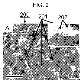
FIG. 2 shows electron micrographs of the complex 2D conductive TiSi2
nanostructure
200 fabricated as described above. FIG. 2A is a scanning electron micrograph
showing the
complex nanostructure 200. The nanostructure 200 is composed of a plurality of
nanonet (NN)
sheets 201. At relatively low magnifications, the nanostructure 200 packs to
resemble tree leaves,
except that each NN sheet 201 is composed of nanobeams 202, as revealed by the
close-up inset.
(Scale bars: 5 m in main frame, and 100 nm in the inset). The nanostructure
200 is better seen
under transmission electron microscope, FIG. 2B. Within each of the NN sheets
201 are
approximately 25 nm wide and approximately 15 nm thick nanobeams 202, all
linked together
by single crystalline junctions with 90 angles. One of the frames is twisted
at the bottom of the
picture (arrow), demonstrating belt-like characteristics.
9
CA 02734673 2011-02-17
WO 2010/025124 PCT/US2009/054864
A series of tilted transmission electron micrographs confirm the 2D
characteristics of
each of the NN sheets 201, as shown in FIG. 2C-2E. The inset electron
diffraction pattern in
FIG. 2C was on the NN sheets 201 in the vertical orientation, revealing the
single crystalline
nature of the NN sheets 201, and that the plane of the NN sheets 201 is
perpendicular to <010>
directions (presence of strong diffraction spot of (060)). Similar series of
tilted images using the
scanning electron microscope, see FIG. 3A-C, shows similar results. As best
seen in FIG. 9B,
2D TiSi2 NN sheets 901 bend and roll up when pushed by a STM tip 910 during
TEM
characterization, further verifying the 2D nature and suggesting that the
nanostructures are
highly flexible as a result of the thinness.
High resolution transmission electron microscopy images and electron
diffraction (ED)
patterns of different regions of the nanobeam 202 from FIG. 2B, reveal that
the entire nanobeam
202 structure is single crystalline, including the 90 joints (FIG. 4A), the
middle (FIG. 4B) and
the ends (FIG. 4C). The ends of the nanobeams 202 within any NN sheet 201, are
free of
impurities, FIG. 4C. Scale bars for FIG. 4A is 5 nm, FIG. 4B is 5 nm, FIG. 4C
is 5 nm, and FIG.
4D is 2 nm. The frames are nanobelts based on two main observations: loose
ends often bend on
TEM supporting films, showing characteristics of nanobeams (see arrow in FIG.
2B), and the
thickness of a NN sheet (approximately 15 nm) is thinner than the width of a
NN sheet
(approximately 25 nm), as evidenced in the tilted TEM image (FIG. 2C, FIG. 3A,
and FIG. 4F).
Further analyses of HRTEM images and associated selected-area electron
diffraction
(SAED) patterns show that the NN sheets 201 are C49 structure with the b axis
perpendicular to
the plane (see FIG. 2C, and FIG. 3A). That is, the NN sheets 201 primarily
grow along a and c
directions. Using a NN sheet having dimensions of 2 m wide and long and 15 nm
thick as an
example, the growth selectivity of different crystal directions (a/b or c/b,
i.e. width/thickness)
>100, a remarkable ratio considering that no growth seeds are involved.
Without being bound by
any particular theory, this can be explained by the orthorhombic symmetry of
C49 TiSi2 and
corresponding atomic arrangements. In a conventional C49 TiSi2 unit cell
(a=3.62A , c=3.61A
and b=13.76A), there exist atomic layers entirely composed of Si along b
direction, which are
less susceptible to depositions of TiSi2 required for continuous crystal
growth (see, FIG. 6). The
Si layer is further passivated by -Cl terminations to protect the {010} planes
from additional
growth, as confirmed by X-ray photoelectron spectroscopy (XPS), see FIG. 4E.
XPS spectra
CA 02734673 2011-02-17
WO 2010/025124 PCT/US2009/054864
from the TiSi2 NN sheets were taken with an Al K-alpha irradiation source
(1486.69 eV) using a
Kratos AXIS Ultra Imaging X-ray Photoelectron Spectrometer with O.leV
resolution. An
internal C is standard was utilized to calibrate the binding energies.
Composition analysis by
XPS shows that Si:Ti ratio on the surface is much greater than 2. This
confirms that Si contents
are richer on the surface, suggesting Si terminations. In contrast, other
planes such as {100} and
{001 } are always composed of both Ti and Si atoms, favoring additions of both
chemical species
and leading to highly anisotropic growth. As a result, 2D structures are
created by promoted
growth of {100} and {001 } planes and inhibited depositions on the {010}
planes.
The sidewalls of the nanobeams are likely passivated by Cl and H as well,
although less
stable than those of the {010} planes. When the passivation is destabilized by
continuous Ti and
Si deposition on the side of a frame, branching occurs. Since TiSi2 preferably
grows along <100>
and <001>, angles between connecting branches are always 90 , yielding the
unique 2D network
nanostructure disclosed herein. When two growing frames meet, one of the
frames either
changes growth direction to form a 90 kink or melts into the second frame to
form a single
crystalline connection (FIG. 8). NN sheets composed of wider, but not thicker,
nanobeams are
obtainable for extended periods of growth (e.g., 1 hr), implying the {100} and
{001} sides are
indeed susceptible to further growth. Noticeably, multiple kinks can be formed
as seen in FIG.
8A. Scale bars 100 nm, 5 nm and 5 nm, from left to right. Arrows in FIG. 8B
and FIG. 8C
indicate the growth direction.
When growth conditions are changed, for example using different pressures,
temperatures
and precursor gas ratios, different structures are obtained. For example, as
shown in FIG. 7, high
quality nanowires (NWs) are also obtainable by using the methods of the
presently disclosed
embodiments and manipulating the growth parameters. The general trend is that
lower pressure,
lower SiH4:TiC14 ratios, and higher temperature favor NWs growth, while the
opposite produces
more NN sheets. Careful studies of the microstructures, however, revealed that
although
belonging to the same symmetry group (orthorhombic), NWs obtained by the
methods of the
presently disclosed embodiments are C54 structure (a=8.236A, b=4.773 A and
c=8.523 A) and
grow along b direction. The structural difference can be confirmed by Raman
spectrum (see
FIG. 7C), as well as TEM characterizations (FIG. 7B). Relatively higher Si
concentrations
(afforded by higher SiH4 ratios, higher pressures, and lower temperatures)
help passivate {010}
planes of the C49 structure and therefore lead to NN sheet growth. The degree
of supersaturation
11
CA 02734673 2011-02-17
WO 2010/025124 PCT/US2009/054864
of TiSi2 in the gas phase can also play a role. The microstructures are
evidenced by the high
resolution imaging, ED patterns, as well as micro-Raman measurements, see FIG.
7C. Raman
spectra were taken on a home-built Raman spectrometer at a laser excitation
wavelength of 647
nm, with a power level of 1 mW and 100x object lens. Scale bars: 5 m in FIG.
7A and 5 nm in
FIG. 7B. TiSi2 nanowires are favored for growth conditions with relatively
lower Si
concentration, e.g. lower pressure and higher temperature.
For bulk TiSi2, C49 phase is reported to form first during solid-state
reactions and then is
converted to C54 at high temperatures (e.g. 700 Q. C49 TiSi2 has been
regarded as the
metastable phase that has higher resistivity, due to stacking faults along the
b direction. It has
been shown that the 2D TiSi2 nanostructures of the presently disclosed
embodiments are
extremely stable-the nanostructure is preserved after up to about 900 C
annealing in H2 for over
30 minutes. The 2D TiSi2 nanostructures of the presently disclosed embodiments
are also highly
conductive. The remarkable stability may result from the small dimensions; 15
nm film thickness
means approximately 10-12 unit cells along <010> direction, within which
stacking faults are
unlikely events.
The complex 2D conductive silicide nanostructures of the presently disclosed
embodiments link low dimensional nanomaterials by high quality single
crystalline junctions,
providing better charge transport between individual components and stronger
mechanical
support. Thus, the complex 2D conductive silicide nanostructures of the
presently disclosed
embodiments are of significant interest for nanoelectronics and emerging solar
energy
harvesting.
Electrical Properties of 2D TiSi2 NN sheets.
FIG. 9 shows electrical measurements of a TiSi2 NN sheet of the presently
disclosed
embodiments. The electrical transport measurements on the TiSi2 NN sheet were
conducted
using a commercial STM-TEM holder (Nanofactory Instruments AB, ST1000). The
NN sheet
was adhered to a sharp and fresh gold needle by gently dragging the needle on
the surface of the
as-prepared sample. Another sharp gold probe was piezo-driven to approach the
nanonets
protruding the gold needle inside the TEM (JOEL 2010F). Electron beams were
blocked during
the measurements to avoid interferences. Care was also taken to minimize air
exposure time
during sample preparation, thus to limit surface oxide growth. When pushed by
the STM tip, the
12
CA 02734673 2011-02-17
WO 2010/025124 PCT/US2009/054864
NN sheet rolled up, see FIG. 9B. The structural change is reversible,
demonstrating a
remarkable flexibility (the structure survives repeatable bending of curves
with radii as small as
less than 500 nm). Scale bar: 500 nm. Current-voltage (I-V) curves were
obtained by applying
biases in the two-terminal configuration, see FIG. 9C. All measurements were
conducted under
vacuum conditions (< 10-5 Pa). The gold probes and needles were obtained by
etching gold wires
(0.010 and 0.013 inches in diameter, respectively) in a 37 weight percent HC1
aqueous solution
with initial etching currents of 2.00 and 2.25 mA, with a bias of
approximately 1 Volt. FIG. 9D
shows how annealing was found necessary to form Ohmic contacts between the STM
tip and
TiSi2 NN sheet of the presently disclosed embodiments. Constant current (50
A) at large bias
(3V) helps from Ohmic contacts.
Electrical resistivity is the resistance of a material in slowing down the
electrical current
when the material is subject to a potential difference. Electrical resistivity
is calculated as:
p = VA/(Ixl), where:
V is the potential difference across the material,
A is the cross-section area,
I is the electrical current flowing through it, and
1 is the length of the material.
Lower resistance leads to lower power consumption and faster responses to
electrical
signals. Lower resistance also allows for higher current as a result of the
lower power
consumption (hence reduced Joule heating.) Electronics built on low-
resistivity materials run
faster under the same power consumption or consumes less power while running
at the same
speed, compared to those made of conventional materials. In energy-related
applications such as
solar cells, lower resistivity yields better efficiencies by reducing energy
lost in transporting
light-induced electricity. As shown in the current-voltage curves, the 2D
TiSi2 NN sheets of the
presently disclosed embodiments are excellent conductors, with low-
resistivity. Assuming the
thickness of 15 nm and width of 30 nm for a single beam within the NN, and
regarding the
charge transport path as shortest distance between contacting electrodes,
e.g.,. about 1 m, the
electrical resistivity of the NN sheets are approximately 10 p ).cm, in good
agreement with that
from bulk C54 and significantly better than bulk C49 TiSiz. Without being
bound by any
13
CA 02734673 2011-02-17
WO 2010/025124 PCT/US2009/054864
particular theory, the absence of defects in the nanostructures of the
presently disclosed
embodiments, which have been determined to be detrimental in electrical
conductance in bulk
C49 TiSi2, may play a role in the nanostructures high current ability.
Methods of fabricating two-dimensional conductive silicides include performing
chemical vapor deposition, wherein one or more gas or liquid precursor
materials carried by a
carrier gas stream react to form a nanostructure having a mesh-like appearance
and including a
plurality of connected and spaced-apart nanobeams linked together at an about
90-degree angle.
The method of the presently disclosed embodiments can be used to synthesize a
new 2D
nanonet structure. The products are high quality single crystalline complex
structures composed
of perpendicular nanobeams. The morphology results from the orthorhombic
crystal symmetry,
and is sensitive to growth conditions; lower Si concentration in the precursor
mixture favors NW
growth. The high quality single crystalline NN sheets disclosed herein
represent one of the most
conductive silicides, and opens new doors to new exciting electronic and
energy-related
applications.
All patents, patent applications, and published references cited herein are
hereby
incorporated by reference in their entirety. It will be appreciated that
several of the above-
disclosed and other features and functions, or alternatives thereof, may be
desirably combined
into many other different systems or applications. Various presently
unforeseen or unanticipated
alternatives, modifications, variations, or improvements therein may be
subsequently made by
those skilled in the art which are also intended to be encompassed by the
following claims.
14