Note : Les descriptions sont présentées dans la langue officielle dans laquelle elles ont été soumises.
CA 02734699 2011-02-17
DESCRIPTION
Power Conversion Apparatus
TECHNICAL FIELD
The present invention relates to a power conversion apparatus for outputting
AC
power based on DC power, such as an uninterruptible power supply system, a
solar
power generation system, a fuel cell power generation system, or a secondary
battery
energy storage system.
BACKGROUND ART
An uninterruptible power supply system has widely been used as a power supply
device for supplying AC power to an important load such as a computer system
in a
stable manner. For example, as disclosed in Japanese Patent Laying-Open No.
2006-
109603 (Patent Document 1), an uninterruptible power supply system generally
includes
a converter for converting AC power to DC power, an'inverter for converting DC
power to AC power, and a capacitor for smoothing DC voltage input to the
inverter.
Usually, the converter converts AC power from a commercial AC power supply to
DC
power, and supplies the DC power to the inverter while charging a power
storage device
such as a storage battery. The inverter converts DC power to AC power and
supplies
the AC power to the load. When the commercial AC power supply fails, power
from
the power storage device is supplied to the inverter, which continues to
supply AC
power to the load.
Patent Document 1: Japanese Patent Laying-Open No. 2006-109603
DISCLOSURE OF THE INVENTION
PROBLEMS TO BE SOLVED BY THE INVENTION
The filter above includes a reactor and a capacitor. When a harmonic is great,
for example, a reactor having great inductance should be used. For example,
the
number of turns of a coil may be increased in order to increase inductance of
the reactor,
-1-
CA 02734699 2011-02-17
however, volume and weight of reactance increase. Therefore, increase in
inductance
of the reactor leads to a problem of increase in volume and weight of the
uninterruptible
power supply system. Japanese Patent Laying-Open No. 2006-109603, however,
does
not show a specific solution to the problem of increase in size of the
uninterruptible
power supply system described above.
In addition, as described in Japanese Patent Laying-Open No. 2006-109603, a
configuration in which a plurality of capacitors are connected in series on
the DC side of
the inverter is not essential in a two-level inverter circuit. When a multi-
level circuit is
used in the inverter, however, a plurality of capacitors must be connected in
series
between a positive terminal and a negative terminal on the DC side of the
inverter. For
example, when the inverter is implemented by a three-level circuit, two
capacitors are
connected in series between the positive electrode terminal and the negative
electrode
terminal on the DC side of the inverter. In addition, wiring is required from
the multi-
level circuit to a point of connection (neutral point) between the two
capacitors. In
this case, since currents flowing through the two capacitors become different
from each
other depending on a current flowing into the neutral point, DC voltages of
both
capacitors can become imbalanced. When the DC voltages of both capacitors
become
imbalanced, an excess voltage may be applied to one capacitor, for example.
Therefore,
when the wiring exists at the neutral point, potential fluctuation at the
neutral point must
be suppressed to equalize the DC voltages of both capacitors. In the
following, control
for equalizing DC voltages of two capacitors will be referred to as "balance
control."
An object of the present invention is to provide a power conversion apparatus
that has a configuration suitable for achieving reduction in size and lighter
weight and
that can achieve balance control over a DC capacitor without adding a special
circuit.
MEANS FOR SOLVING THE PROBLEMS
According to one aspect of the present invention, a power conversion apparatus
includes first, second and third conversion devices and a filter. The first
conversion
device includes a first multi-level circuit configured to be able to perform
conversion
-2-
CA 02734699 2011-02-17
between a DC voltage and an AC voltage varying among at least three voltage
values,
and converts DC power to AC power for supply to a load. The second conversion
device converts AC power from an AC power supply to DC power for supply to the
first conversion device. The third conversion device converts a voltage value
of power
stored in a power storage device and supplies DC power from the power storage
device
to the first conversion device when power supply by the AC power supply is
abnormal.
The filter includes a reactor and a capacitor and removes a harmonic generated
by the
first conversion device.
According to another aspect of the present invention, a power conversion
apparatus includes first and second capacitors, a second multi-level circuit,
a DC power
supply source, a third multi-level circuit, and a control device. The first
and second
capacitors are connected in series between a DC positive bus and a DC negative
bus.
The second multi-level circuit is connected to the DC positive bus, the DC
negative bus
and a neutral point between the first and second capacitors, for converting AC
power
supplied from an AC power supply to an input end to DC power and outputting
the DC
power to between the DC positive bus and the DC negative bus. The third multi-
level
circuit is connected to the DC positive bus, the DC negative bus and the
neutral point in
parallel to the second multi-level circuit, for converting a voltage of DC
power supplied
from the DC power supply source to the input end and outputting the DC power
to
between the DC positive bus and the DC negative bus. The control device
controls
operation of the second and third multi-level circuits to suppress potential
fluctuation at
the neutral point.
EFFECTS OF THE INVENTION
According to the present invention, reduction in size and lighter weight of
the
power conversion apparatus can be achieved, and balance control over the DC
capacitor
can be achieved without adding a special circuit.
BRIEF DESCRIPTION OF THE DRAWINGS
Fig. 1 is a schematic block diagram showing a main circuit configuration of an
-3-
CA 02734699 2011-02-17
uninterruptible power supply system 100 according to an embodiment of the
present
invention.
Fig. 2 is a circuit diagram illustrating in detail a configuration of a
converter 3
and an inverter 4 shown in Fig. 1.
Fig. 3 is a diagram illustrating in detail a configuration of a DC voltage
converter
7 shown in Fig. 1.
Fig. 4 is a block diagram illustrating control units of converter 3 and DC
voltage
converter 7 included in a control device 10.
Fig. 5 is a functional block diagram of a voltage instruction generation
circuit 61
shown in Fig. 4.
Fig. 6 is a functional block diagram of a voltage instruction generation
circuit 71
shown in Fig. 4.
Fig. 7 is a diagram showing a single-phase inverter implemented by a two-level
circuit.
Fig. 8 is an equivalent circuit of an inverter 41 shown in Fig. 7.
Fig. 9 is a diagram showing a line voltage of inverter 41.
Fig. 10 is an equivalent circuit diagram of a U-phase arm 4U and a V-phase arm
4V of inverter 4 shown in Fig. 2.
Fig. 11 is a diagram showing a line voltage of a single-phase, three-level
inverter
shown in Fig. 10.
Fig. 12 is a diagram showing a result of simulation of a reactor current in an
example where a filter reactor provided on an output side of a two-level
inverter is set to
5% and the inverter is switched at a frequency of 10 kHz.
Fig. 13 is a diagram showing a result of simulation of a reactor current in an
example where a filter reactor provided on an output side of a two-level
inverter is set to
10% and the inverter is switched at a frequency of 10 kHz.
Fig. 14 is a diagram showing a result of simulation of a reactor current in an
example where a filter reactor provided on an output side of a three-level
inverter is set
-4-
CA 02734699 2011-02-17
to 5% and the inverter is switched at a frequency of 10 kHz.
Fig. 15 is a diagram showing a frequency spectrum of a harmonic current (Fig.
12) generated by the two-level inverter.
Fig. 16 is a diagram showing a frequency spectrum of a harmonic current (Fig.
14) generated by the three-level inverter.
Fig. 17 is a diagram showing a result of simulation of fluctuation of a
potential to
ground of the two-level inverter and fluctuation of a potential to ground of
the three-
level inverter.
Fig. 18 is a diagram showing a result of simulation of loss in the two-level
inverter and the three-level inverter.
Fig. 19 is a diagram illustrating a breakdown of the loss in the two-level
inverter
and the three-level inverter.
Fig. 20 is a diagram showing a configuration of a semiconductor switch
included
in a conventional DC voltage converter.
Fig. 21 is a diagram showing a switching pattern of IGBT elements Q1D to Q4D
in Fig. 3 and a voltage applied to a reactor 22.
Fig. 22 is an equivalent circuit diagram showing a configuration of two phases
of
converter 3 shown in Fig. 2.
Fig. 23 is a signal waveform diagram for illustrating PWM control over one
phase of converter 3 (three-level PWM converter) by a converter control unit
53 shown
in Fig. 4.
Fig. 24 is a diagram showing a switching pattern of four IGBT elements
included
in an arm of each phase of the converter, in each mode.
Fig. 25 is a diagram showing a circuit of one phase and a current route in the
circuit in each mode shown in Fig. 24.
Fig. 26 is a signal waveform diagram for illustrating balance control by
converter
3 when Ep < En.
Fig. 27 is a signal waveform diagram for illustrating balance control by
converter
-5-
CA 02734699 2011-02-17
3 when Ep > En.
Fig. 28 is a signal waveform diagram for illustrating PWM control over a
semiconductor switch 23 by a semiconductor switch control unit 54 shown in
Fig. 4.
Fig. 29 is a diagram showing a switching pattern of IGBT elements QID to Q4D
included in semiconductor switch 23.
Fig. 30 is a diagram showing a circuit and a current route in the circuit in
each
mode shown in Fig. 29.
Fig. 31 is a signal waveform diagram for illustrating balance control by
semiconductor switch 23 when Ep < En.
Fig. 32 is a signal waveform diagram for illustrating balance control by
semiconductor switch 23 when Ep > En.
Fig. 33 is a diagram showing a state that a power conversion apparatus
according to the present invention is applied to a three-phase, four-wire
system.
DESCRIPTION OF THE REFERENCE SIGNS
1 commercial AC power supply; 2 input filter; 3 converter; 3R R-phase arm; 3 S
S-phase arm; 3T T-phase arm; 4 inverter; 4U U-phase arm; 4V V-phase arm; 4W W-
phase arm; 5 output filter; 6 load; 7 DC voltage converter; 8 storage battery;
10 control
device; 11, 11R, 11S, 11T, 15, 16, 19, 19U, 19V, 19W capacitor; 12, 12R, 12S,
12T,
18, 18U, 18V, 18W, 22, 22N, 22P, 45 reactor; 13 DC positive bus; 14 DC
negative bus;
17 DC neutral point bus; 21 neutral point; 23, 44 semiconductor switch; 31,
34, 35, 36
voltage sensor; 32, 37 current sensor; 33 power failure detection circuit; 51,
63A to 63C,
73A, 88A to 88C adder; 52, 82, 86A to 86C, 73B, 82, 92, 94 subtractor; 53
converter
control unit; 54 semiconductor switch control unit; 61, 71 voltage instruction
generation
circuit; 62, 72 neutral point potential control circuit; 64, 74 stop circuit;
64A to 64C,
74A, 74B switch; 65 PWM circuit; 75 PWM circuit; 81, 91 reference value
generation
circuit; 83 DC voltage control circuit; 84 sinusoidal wave generation circuit;
85A to 85C
multiplier; 87, 95 current control circuit; 93 voltage control circuit; 100
uninterruptible
power supply system; 101, 102, 151, 152 reference signal; 103 to 105, 153 to
155
-6-
CA 02734699 2011-02-17
voltage instruction signal; 106 to 108 phase voltage; 111 to 114, 121 to 124,
131 to 134,
161 to 164, 171 to 174, 181 to 184 switching pattern; 141 input phase voltage;
142
phase current; CA, CB, CC, CD capacitor; DID to D4D, D1R to D6R, D1S to D6S,
D 1 T to D6T, D 1U to D6U, D 1 V to D6V, D 1 W to D6W, DA, DB, DC, DD diode;
Q1D to Q4D, Q1R to Q4R, Q1S to Q4S, Q1T to Q4T, Q1U to Q4U, Q1V to Q4V,
Q 1 W to Q4W, QA, QB, QC, QD IGBT element; RL R-phase line; SL S-phase line;
TL
T-phase line; UL U-phase line; VL V-phase line; and WL W-phase line.
BEST MODES FOR CARRYING OUT THE INVENTION
An embodiment of the present invention will be described hereinafter in detail
with reference to the drawings. It is noted that the same or corresponding
elements in
the drawings have the same reference characters allotted and description
thereof will not
be repeated.
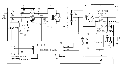
Fig. 1 is a schematic block diagram showing a main circuit configuration of an
uninterruptible power supply system 100 according to an embodiment of the
present
invention. Referring to Fig. 1, uninterruptible power supply system 100
includes an
input filter 2, a converter 3, an inverter 4, an output filter 5, a DC voltage
converter
(denoted as "DC/DC" in the drawing) 7, a control device 10, a DC positive bus
13, a
DC negative bus 14, capacitors 15 and 16, a DC neutral point bus 17, voltage
sensors
31, 34, 35, and 36, current sensors 32 and 37, a power failure detection
circuit 33, an R-
phase line RL, an S-phase line SL, and a T-phase line TL.
Input filter 2 prevents leakage of harmonics to a commercial AC power supply
1.
Commercial AC power supply 1 is a three-phase AC power supply. Input filter 2
is a
three-phase LC filter circuit constituted of a capacitor 11 (capacitors 11R,
11 S and 11 T)
and a reactor 12 (reactors 12R, 12S and 12T).
Converter 3 converts three-phase AC power supplied from commercial AC
power supply 1 through input filter 2 into DC power and supplies the DC power
to
inverter 4 through DC positive bus 13 and DC negative bus 14. Inverter 4
converts the
DC power from converter 3 into three-phase AC power. As will be described
later,
-7-
CA 02734699 2011-02-17
converter 3 and inverter 4 are each implemented by a three-level circuit.
Converter 3
and inverter 4 are connected to each other through DC positive bus 13, DC
negative bus
14 and DC neutral point bus 17.
Capacitors 15 and 16 are connected in series between DC positive bus 13 and
DC negative bus 14 and they smooth a voltage across DC positive bus 13 and DC
negative bus 14. DC neutral point bus 17 is connected to a neutral point 21
which is a
point of connection between capacitors 15 and 16.
The AC power from inverter 4 is supplied to a load 6 through output filter 5.
Output filter 5 removes harmonics generated by an operation of inverter 4.
Output
filter 5 is a three-phase LC filter circuit constituted of a reactor 18
(reactors 18U, 18V
and 18W) and a capacitor 19 (capacitors 19U, 19V and 19W).
DC voltage converter 7 converts a voltage of a storage battery 8 to a DC
voltage across DC positive bus 13 and DC negative bus 14. It is noted that DC
voltage converter 7 may be configured to carry out conversion between the DC
voltage
across DC positive bus 13 and DC negative bus 14 and the voltage of storage
battery 8.
In addition, a power storage device that can be charged and can discharge
should only
be connected to DC voltage converter 7, and for example, an electric double
layer
capacitor may be connected to DC voltage converter 7. In addition, though
storage
battery 8 is installed outside uninterruptible power supply system 100 in the
present
embodiment, storage battery S may be contained in uninterruptible power supply
system
100.
Voltage sensor 31 detects a voltage VR of the R-phase line, a voltage VS of
the
S-phase line, and a voltage VT of the T-phase line, and outputs three-phase
voltage
signals indicating respective voltages VR, VS and VT to control device 10 and
power
failure detection circuit 33. Current sensor 32 detects a current IR of the R-
phase line,
a current IS of the S-phase line, and a current IT of the T-phase line and
outputs three-
phase current signals indicating respective voltages IR, IS and IT to control
device 10.
Power failure detection circuit 33 detects power failure of commercial AC
power
-8-
CA 02734699 2011-02-17
supply 1 based on the three-phase voltage signal from voltage sensor 31. Power
failure
detection circuit 33 outputs a power failure signal indicating power failure
of
commercial AC power supply 1 to control device 10.
The voltage across DC positive bus 13 and DC negative bus 14 is divided into
voltages Ep and En at neutral point 21. Voltage sensor 34 detects voltage Ep
across
opposing ends of capacitor 15 and outputs a signal indicating voltage Ep to
control
device 10. Voltage sensor 35 detects voltage En across opposing ends of
capacitor 16
and outputs a signal indicating voltage En to control device 10, Voltage
sensor 36
detects a voltage VB across positive and negative electrodes of storage
battery 8 and
outputs a signal indicating voltage VB to control device 10. Current sensor 37
detects
a current IB output from storage battery 8 and outputs a signal indicating
current IB to
control device 10.
Control device 10 controls operations of converter 3, inverter 4 and DC
voltage
converter 7. Though detailed description will be provided later, each of
converter 3,
inverter 4 and DC voltage converter 7 is implemented by a semiconductor switch
including a semiconductor switching element. In the present embodiment, an
IGBT
(Insulated Gate Bipolar Transistor) is employed as the semiconductor switching
element.
In addition, in the present embodiment, PWM (Pulse Width Modulation) control
is
applicable as a method of controlling the semiconductor switching element.
Control
device 10 carries out PWM control, upon receiving the three-phase voltage
signal from
voltage sensor 3 1, the three-phase current signal from current sensor 32, the
signal
indicating voltage Ep detected by voltage sensor 34, the signal indicating
voltage En
detected by voltage sensor 3 5, the power failure signal from power failure
detection
circuit 33, the signal indicating voltage VB detected by voltage sensor 36,
the signal
indicating current IB detected by current sensor 37, and the like.
An operation of uninterruptible power supply system 100 according to the
present embodiment will now be described. When commercial AC power supply 1
can
normally supply AC power, converter 3 converts AC power from commercial AC
power
-9-
CA 02734699 2011-02-17
supply 1 to DC power and inverter 4 converts the DC power into AC power and
supplies the AC power to load 6. On the other hand, when the commercial AC
power
supply fails, control device 10 stops converter 3 based on the power failure
signal from
power failure detection circuit 33. In addition, control device 10 operates DC
voltage
converter 7 such that DC power is supplied from storage battery 8 to inverter
4, thus
causing inverter 4 to continue supply of AC power. Here, DC voltage converter
7
converts the voltage of storage battery 8 into a voltage suitable as an input
voltage for
inverter 4. Thus, AC power can be supplied to an AC load in a stable manner.
Fig. 2 is a circuit diagram illustrating in detail a configuration of
converter 3 and
inverter 4 shown in Fig. 1. Referring to Fig. 2, converter 3 includes an R-
phase arm
3R, an S-phase arm 3S and a T-phase arm 3T. Inverter 4 includes all-phase arm
4U,
a V-phase arm 4V and a W-phase arm 4W.
The arm of each phase (3R, 3 S, 3 T) of converter 3 and the arm of each phase
(4U, 4V, 4W) of inverter 4 are each implemented by a three-level circuit, and
each of
them includes four IGBT elements and six diodes. Specifically, R-phase arm 3R
includes IGBT elements QIR to Q4R and diodes DIR to D6R. S-phase arm 3S
includes IGBT elements Q1S to Q4S and diodes DIS to D6S. T-phase arm 3T
includes IGBT elements Q 1 T to Q4T and diodes D 1 T to D6T. U-phase arm 4U
includes IGBT elements Q1U to Q4U and diodes D1U to D6U. V-phase arm 4V
includes IGBT elements Q1V to Q4V and diodes DIV to D6V. W-phase arm 4W
includes IGBT elements Q I W to Q4W and diodes D 1 W to D6W.
Hereinafter, in order to collectively describe the arm of each phase of
converter
3 and the arm of each phase of inverter 4, reference characters R, S, T, U, V,
and W are
collectively denoted as a reference character "x". IGBT elements Qlx to Q4x
are
connected in series between DC positive bus 13 and DC negative bus 14. Diodes
Dlx
to D4x are connected in anti-parallel to IGBT elements Q I x to Q4x,
respectively.
Diode D5x is connected to a point of connection between IGBT elements QIx and
Q2x
and neutral point 21. Diode D6x is connected to a point of connection between
IGBT
-10-
CA 02734699 2011-02-17
elements Q3x and Q4x and neutral point 21. It is noted that diode D5x has a
cathode
connected to the point of connection between IGBT elements Q lx and Q2x and
has an
anode connected to neutral point 21. Diode D6x has an anode connected to the
point
of connection between IGBT elements Q3x and Q4x and has a cathode connected to
neutral point 21. Diodes Dlx to D4x function as free-wheeling diodes, and
diodes D5x
and D6x function as clamp diodes.
In the arm of each phase (3R, 3S, 3T) of converter 3, a point of connection
between IGBT elements Q2x and Q3x corresponds to an AC input terminal, and a
point
of connection between diodes D5x and D6x corresponds to a DC output terminal.
Meanwhile, in the arm of each phase (4U, 4V, 4T) of inverter 4, the point of
connection
between diodes D5x and D6x corresponds to a DC input terminal, and the point
of
connection between IGBT elements Q2x and Q3x corresponds to an AC output
terminal.
The AC input terminal of the arm of each phase (3R, 3 S, 3 T) of converter 3
is
connected to a corresponding line (R-phase line RL, S-phase line SL, T-phase
line TL),
and the AC output terminal of the arm of each phase (4U, 4V, 4S) of inverter 4
is
connected to a corresponding line (U-phase line UL, V-phase line VL, W-phase
line
WL). The DC output terminal of the arm of each phase of converter 3 and the DC
input terminal of the arm of each phase of inverter 4 are connected to neutral
point 21.
Fig. 3 is a diagram illustrating in detail a configuration of DC voltage
converter 7
shown in Fig. 1. Referring to Fig. 3, DC voltage converter 7 includes a
reactor 22 and
a semiconductor switch 23. Semiconductor switch 23 includes IGBT elements QID
to
Q4D connected in series between DC positive bus 13 and DC negative bus 14 and
diodes DID to D4D connected in anti-parallel to IGBT elements QID to Q4D,
respectively.
In semiconductor switch 23, one end of a reactor 22P is connected to a point
of
connection between IGBT elements QID and Q2D and one end of a reactor 22N is
connected to a point of connection between IGBT elements Q3D and Q4D. The
other
end of reactor 22P is connected to the positive electrode of storage battery 8
and the
-11-
CA 02734699 2011-02-17
other end of reactor 22N is connected to the negative electrode of storage
battery 8.
Fig. 4 is a block diagram illustrating control units of converter 3 and DC
voltage
converter 7 included in control device 10. Referring to Fig. 4, control device
10
includes an adder 51, a subtractor 52, a converter control unit 53, and a
semiconductor
switch control unit 54. Adder 51 adds voltage value Ep indicating a voltage of
capacitor 15 detected by voltage sensor 34 and value En of a voltage of
capacitor 16
detected by voltage sensor 35, and outputs a voltage value (Ep + En) across DC
positive bus 13 and DC negative bus 14. Subtractor 52 subtracts voltage value
En
from voltage value Ep and outputs a value of voltage difference (Ep - En).
Converter control unit 53 includes a voltage instruction generation circuit
61, a
neutral point potential control circuit 62, adders 63A to 63C, a stop circuit
64, and a
PWM circuit 65. Upon receiving voltages VR, VS and VT detected by voltage
sensor
31, currents IR, IS and IT detected by current sensor 32, and voltage value
(Ep + En)
calculated by adder 51, voltage instruction generation circuit 61 generates
voltage
instruction values VRo*, VSo* and VTo* corresponding to the R phase, the S
phase and
the T phase, respectively. Upon receiving the value indicating voltage
difference (Ep -
En) from subtractor 52, neutral point potential control circuit 62 generates a
voltage
instruction value V,*. For example, neutral point potential control circuit 62
generates
voltage instruction value V1* by proportional operation or proportional
integral
operation of voltage difference (Ep - En).
Adder 63A adds voltage instruction values VRo* and Vl* and generates a voltage
instruction value VR*. Adder 63B adds voltage instruction values VSO* and Vj*
and
generates a voltage instruction value VS*. Adder 63C adds voltage instruction
values
VTo* and Vl* and generates a voltage instruction value VT*.
Stop circuit 64 includes switches 64A to 64C. When a signal from power
failure detection circuit 33 indicates that commercial AC power supply I is
normal (for
example, when a logical value of the signal is "1 "), switches 64A to 64C are
set such
that voltage instruction values VR*, VS* and VT* are transmitted to PWM
circuit 65.
-12-
CA 02734699 2011-02-17
When the signal from power failure detection circuit 33 indicates power
failure of
commercial AC power supply I (for example, when a logical value of the signal
is 110"),
switches 64A to 64C are all grounded. As a result, input of the voltage
instruction
values to PWM circuit 65 stops, and at the same time, an OFF signal is
provided to all
IGBT elements of converter 3 and converter 3 stops.
Based on voltage instruction values VR*, VS* and VT*, PWM circuit 65 outputs
a signal for equalizing voltages VR, VS and VT detected by voltage sensor 31
and
voltage instruction values VR*, VS* and VT*, respectively. This signal is for
driving
the four IGBT elements included in the arm of each phase of converter 3.
Semiconductor switch control unit 54 includes a voltage instruction generation
circuit 71, a neutral point potential control circuit 72, an adder 73A, a
subtractor 73B, a
stop circuit 74, and a PWM circuit 75.
Upon receiving voltage VB detected by voltage sensor 36, current IB detected
by current sensor 37 and voltage value (Ep + En) calculated by adder 51,
voltage
instruction generation circuit 71 generates a voltage instruction value V* for
controlling
voltage values Ep and En to prescribed voltages.
Upon receiving the value indicating voltage difference (Ep - En) from
subtractor
52, neutral point potential control circuit 72 generates a voltage instruction
value VB1*.
For example, neutral point potential control circuit 72 generates voltage
instruction
value VB1* by proportional operation or proportional integral operation of
voltage
difference (Ep - En). For example, when Ep - En > 0, neutral point potential
control
circuit 72 sets voltage instruction value VB1* to a negative value. On the
other hand,
when Ep - En < 0, neutral point potential control circuit 72 sets voltage
instruction
value VB1* to a positive value.
Adder 73A adds voltage instruction values V* and VB1* and generates a voltage
instruction value VA*. Subtractor 73B subtracts voltage instruction value VB1*
from
voltage instruction value V* and generates a voltage instruction value VB*.
Voltage
-13-
CA 02734699 2011-02-17
instruction values VA* and VB* are instruction values for controlling voltages
of an
upper arm and a lower arm of semiconductor switch 23, respectively, and
instruction
values of voltages Ep and En for making a difference between voltages Ep and
En zero.
Neutral point potential control circuit 72, adder 73A and subtractor 73B
configure an
instruction value generation circuit that generates voltage instruction values
VA* and
VB* for controlling voltages Ep and En, respectively, to make voltage
difference (Ep -
En) zero based on voltage difference (Ep - En) and voltage instruction value
V*.
Stop circuit 74 includes switches 74A and 74B. When the signal from power
failure detection circuit 33 indicates that commercial AC power supply 1 is
normal,
switches 74A and 74B are all grounded. As a result, input of the voltage
instruction
values to PWM circuit 75 stops, and at the same time, an OFF signal is
provided to all
IGBT elements of DC voltage converter 7 and DC voltage converter 7 stops. On
the
other hand, when the signal from power failure detection circuit 33 indicates
power
failure of commercial AC power supply 1, switches 74A and 74B are set such
that
voltage instruction values VA* and VB* are transmitted to PWM circuit 75 and
an
ON/OFF instruction is provided to the IGBT elements of DC voltage converter 7.
PWM circuit 75 outputs a signal for driving the four IGBT elements included in
semiconductor switch 23, based on voltage instruction values VA* and VB*.
Fig. 5 is a functional block diagram of voltage instruction generation circuit
61
shown in Fig. 4. Referring to Fig. 5, voltage instruction generation circuit
61 includes
a reference value generation circuit 81, subtractors 82 and 86A to 86C, a DC
voltage
control circuit 83, a sinusoidal wave generation circuit 84, multipliers 85A
to 85C, and a
current control circuit 87.
Reference value generation circuit 81 generates a reference value Eref which
is a
reference value of voltage value (Ep + En). Subtractor 82 calculates a
difference
between reference value Eref and voltage value (Ep + En) generated by adder
51. DC
voltage control circuit 83 calculates a current instruction value I* for
controlling a
current flowing to the input side of converter 3 to make the difference
between
-14-
CA 02734699 2011-02-17
reference value Eref and voltage value (Ep + En) zero. DC voltage control
circuit 83
calculates current instruction value I* by proportional operation or
proportional integral
operation of an error between the reference value and the detected voltage
value, for
example.
Sinusoidal wave generation circuit 84 outputs a sinusoidal wave signal of the
same phase as an R-phase voltage of commercial AC power supply 1, a sinusoidal
wave
signal of the same phase as an S-phase voltage of commercial AC power supply
1, and a
sinusoidal wave signal of the same phase as a T-phase voltage of commercial AC
power
supply 1. The three sinusoidal wave signals are input to multipliers 85A to
85C,
respectively, and are multiplied by current instruction value I*. As a result,
current
instruction values IR*, IS* and IT* of the same phase as the phase voltage of
commercial
AC power supply 1 are generated.
Subtractor 86A calculates a difference between current instruction value IR*
and
R-phase current IR detected by current sensor 32. Subtractor 86B calculates a
difference between current instruction value IS* and S-phase current IS
detected by
current sensor 32. Subtractor 86C calculates a difference between current
instruction
value IT* and T-phase current IT detected by current sensor 32.
Current control circuit 87 generates voltage instruction values VRa*, VSa* and
VTa* as a voltage to be applied to reactor 32 such that all of the difference
between
current instruction value IR* and R-phase current IR, the difference between
current
instruction value IS* and S-phase current IS, and the difference between
current
instruction value IT* and T-phase current IT become zero. Current control
circuit 87
generates the voltage instruction value by amplifying the difference between
the current
value detected by the current sensor and the current instruction value in
accordance with
proportional control or proportional integral control, for example.
An adder 88A adds voltage instruction value VRa* and R-phase voltage VR
detected by voltage sensor 31 and generates voltage instruction value VRo*. An
adder
- 15 -
CA 02734699 2011-02-17
88B adds voltage instruction value VSa* and S-phase voltage VS detected by
voltage
sensor 31 and generates voltage instruction value VSO*. An adder 88C adds
voltage
instruction value VTa* and T-phase voltage VT detected by voltage sensor 31
and
generates voltage instruction value VTo*.
Converter control unit 53 having the above configuration controls converter 3,
and thus, currents IR, IS and IT become currents having sinusoidal waves and
the same
phase as commercial AC power supply 1. Therefore, the power factor can be set
to
substantially 1.
Fig. 6 is a functional block diagram of voltage instruction generation circuit
71
shown in Fig. 4. Referring to Fig. 6, voltage instruction generation circuit
71 includes
a reference value generation circuit 91, a subtractor 92, a voltage control
circuit 93, an
adder 94, and a current control circuit 95. Reference value generation circuit
91
generates reference value Eref which is the reference value of voltage value
(Ep + En).
Subtractor 92 calculates a difference between reference value Eref and voltage
value
(Ep + En) generated by adder 51. Voltage control circuit 93 calculates a
current
instruction value IB* corresponding to the difference between reference value
Eref and
voltage value (Ep + En), based on voltage VB of storage battery 8 detected by
voltage
sensor 36. Voltage control circuit 93 calculates current instruction value IB*
by
proportional operation or proportional integral operation of an error between
the
reference value and the detected voltage value, for example. Adder 94
subtracts
current instruction value IB* generated by voltage control circuit 93 and
current value
IB of storage battery 8 detected by current sensor 37. Current control circuit
95
generates voltage instruction value V' based on the difference between current
instruction value IB` and current value IB.
In uninterruptible power supply system 100 according to the present
embodiment, converter 3 and inverter 4 are each implemented by a three-level
circuit.
In a conventional power conversion apparatus, for the purpose of, for example,
reducing
the number of semiconductor switching elements, an inverter is generally
implemented
-16-
CA 02734699 2011-02-17
by a two-level circuit. By implementing the inverter with the three-level
circuit,
harmonics can be suppressed more than in the conventional power conversion
apparatus.
Fig. 7 is a diagram showing a single-phase inverter implemented by a two-level
circuit. Referring to Fig. 7, an inverter 41 includes a U-phase arm 41U and a
V-phase
arm 41 V. U-phase arm 41U and V-phase arm 41V are connected in parallel
between a
DC positive bus 42 and a DC negative bus 43 and they are identical in
configuration.
U-phase arm 41U includes IGBT elements QA and QB connected in series between
DC
positive bus 42 and DC negative bus 43 and diodes DA and DB connected in anti-
parallel to IGBT elements QA and QB, respectively. U-phase line UL is
connected to
a point of connection between IGBT elements QA and QB. V-phase arm 41 V has
such a configuration that U-phase line UL in the configuration of U-phase arm
41U
above is replaced with V-phase line VL.
Capacitors CA and CB are connected in series between DC positive bus 42 and
DC negative bus 43. A neutral point 0 is a point of connection between
capacitors CA
and CB. A voltage across opposing ends of capacitor CA and a voltage across
opposing ends of capacitor CB are both E/2 (E being a prescribed value).
Fig. 8 is an equivalent circuit of inverter 41 shown in Fig. 7. Referring to
Fig. 8,
U-phase arm 41U is equivalent to a switch that switches connection of U-phase
line UL
between DC positive bus 42 and DC negative bus 43. Considering an example
where
neutral point 0 is grounded, when the switch operates, a voltage Vu of U-phase
line UL
switches between E/2 and -E/2. A voltage Vv of V-phase line VL varies
similarly to
voltage Vu. Thus, the two-level circuit converts a DC voltage E to an AC
voltage
having two values (E/2, -E/2).
Fig. 9 is a diagram showing a line voltage of inverter 41. Referring to Fig.
9, a
line voltage (a difference between voltage Vu and voltage Vv) switches between
E, 0,
and -E. In an inverter implemented by a two-level circuit (a two-level
inverter), a
minimum variation of the line voltage is equal to voltage E.
Fig. 10 is an equivalent circuit diagram of U-phase arm 4U and V-phase arm 4V
-17-
CA 02734699 2011-02-17
of inverter 4 shown in Fig. 2. Referring to Fig. 10, U-phase arm 4U is
equivalent to a
switch that switches connection of U-phase line UL between DC positive bus 13,
neutral
point 21, and DC negative bus 14. When this switch operates, voltage Vu of U-
phase
line UL switches between E/2, 0 and -E/2. Voltage Vv of V-phase line VL also
varies
similarly to voltage Vu. Thus, the three-level circuit is a circuit capable of
performing
conversion between a DC voltage and an AC voltage having three values.
Fig. 11 is a diagram showing a line voltage of a single-phase, three-level
inverter
shown in Fig. 10. Referring to Fig. 11, the line voltage (a difference between
voltage
Vu and voltage Vv) switches in a range of E, E/2, 0, -E/2, and -E. In an
inverter
implemented by a three-level circuit (a three-level inverter), a minimum
variation of the
line voltage is equal to E/2.
It can be seen from Figs. 9 and 11 that the three-level inverter is smaller in
variation of the line voltage than the two-level inverter. Since a waveform of
an output
voltage of the inverter finely varies as the variation of the line voltage is
smaller, the
waveform can be closer to a sinusoidal wave. As the voltage waveform is closer
to the
sinusoidal wave, harmonics generated by the operation of the inverter can be
made
smaller. Therefore, harmonics can be made smaller by the three-level inverter
than the
two-level inverter.
Fig. 12 is a diagram showing a result of simulation of a reactor current in an
example where a filter reactor provided on an output side of a two-level
inverter is set to
5% and the inverter is switched at a frequency of 10 kHz. Fig. 13 is a diagram
showing a result of simulation of a reactor current in an example where a
filter reactor
provided on an output side of a two-level inverter is set to 10% and the
inverter is
switched at a frequency of 10 kHz. Comparing total harmonic distortion (THD)
based
on simulation in Figs. 12 and 13, THD is 6.4% when reactor inductance is set
to 5%,
whereas THD decreases to 3.2% by increasing reactor inductance to 10%.
THD represents a ratio between the sum of effective values of harmonic
components and effective values of fundamental waves. Smaller THD means
smaller
-18-
CA 02734699 2011-02-17
harmonic components. Figs. 12 and 13 show that THD decreases by increasing
reactor
inductance. If reactor inductance is increased in order to make the harmonic
components smaller, it is necessary, for example, to increase the number of
turns of a
coil, and a problem of increase in volume and weight of the reactor arises.
Fig. 14 is a diagram showing a result of simulation of a reactor current in an
example where a filter reactor provided on an output side of a three-level
inverter is set
to 5% and the inverter is switched at a frequency of 10 kHz. Referring to
Figs. 14 and
12, it can be seen that the three-level inverter can suppress harmonic
components more
than the two-level inverter provided that filter reactors are identical in
inductance. In
the simulation result shown in Fig. 14, THD was 3.2%.
Fig. 15 is a diagram showing a frequency spectrum of a harmonic current (Fig.
12) generated by the two-level inverter. Fig. 16 is a diagram showing a
frequency
spectrum of a harmonic current (Fig. 14) generated by the three-level
inverter.
Referring to Figs. 15 and 16, it can be seen that the three-level inverter can
suppress
harmonics more than the two-level inverter, regardless of a frequency. It is
noted that
frequency spectra in Figs. 15 and 16 could be obtained by simulation. In
simulation, a
DC voltage input to the inverter was set to 500 V, a three-phase resistance
load of 10
kW was adopted as a load, and an output voltage (line voltage) was set to 208
Vrms.
Thus, according to the present embodiment, by implementing an inverter with a
three-level circuit, harmonics generated by the inverter can be made smaller.
As a
reactor having small inductance can thus be used for the filter, the reactor
can have
smaller volume and weight. Therefore, according to the present embodiment,
reduction in size and lighter weight of the power conversion apparatus can be
achieved.
In the present embodiment, the following effects can also be obtained by
implementing an inverter with a three-level circuit. In the power conversion
apparatus,
a storage battery or the like having large capacity is connected, as a DC
power supply,
to a DC capacitor on the input side of the inverter. When fluctuation of a
potential to
ground becomes greater during operation of the inverter, an amount of
generated noise
-19-
CA 02734699 2011-02-17
increases due to a large stray capacitance of a DC circuit. Since variation of
the output
voltage becomes greater by implementing inverter 4 with a two-level inverter,
fluctuation of a potential to ground also becomes greater. In the present
embodiment,
however, by implementing inverter 4 with a three-level inverter, variation of
the output
voltage thereof can be made smaller than in a case of a two-level inverter. As
fluctuation of a potential to ground can thus be made smaller, an amount of
generated
noise can be decreased.
Fig. 17 is a diagram showing a result of simulation of fluctuation of a
potential to
ground of the two-level inverter and fluctuation of a potential to ground of
the three-
level inverter. In simulation, a DC voltage input to the inverter was set to
360 V.
Referring to Fig. 17, assuming fluctuation of a potential to ground in the two-
level
inverter as 1 [p.u], fluctuation of a potential to ground in the three-level
inverter is 0.5
[p.u]. As shown in Fig. 17, the three-level inverter can achieve smaller
fluctuation of a
potential to ground.
In addition, according to the present embodiment, loss in inverter 4 can be
decreased. Loss in inverter 4 specifically refers to conduction loss (loss in
each of the
IGBT element and the diode when they are fed with power) and switching loss in
the
IGBT element.
Fig. 18 is a diagram showing a result of simulation of loss in the two-level
inverter and the three-level inverter. Fig. 19 is a diagram illustrating a
breakdown of
the loss in the two-level inverter and the three-level inverter. In this
simulation, a DC
input voltage was set to 600 V, a switching frequency was set to 10 kHz, an AC
output
voltage (line voltage) was set to 380 Vrms, and magnitude of a load was set to
275 kW.
It is noted that the IGBT element included in the two-level inverter is a
1200V-600A
product and the IGBT element included in the three-level inverter is a 600V-
600A
product.
Referring to Figs. 18 and 19, the entire loss in the three-level inverter is
equal to
83% of the entire loss in the two-level inverter, because switching loss is
decreased.
-20-
CA 02734699 2011-02-17
As shown in Fig. 18, the three-level inverter is smaller in switching loss
than the two-
level inverter (33%), because a voltage applied to a single semiconductor
switching
element can be lowered in the three-level inverter as compared with the two-
level
inverter.
As shown in Fig. 19, in the two-level inverter, switching loss occupies most
(63%) of the entire loss. The three-level inverter can achieve significant
decrease in the
switching loss. Therefore, in the three-level inverter, though conduction loss
increases
as compared with the two-level inverter, the entire loss can be smaller than
in the two-
level inverter. By decreasing loss in the inverter, operation efficiency of
the power
conversion apparatus can be enhanced.
In the present embodiment, since converter 3 is also implemented by a three-
level circuit, an effect the same as in inverter 4 can also be achieved by
converter 3.
Specifically, a reactor included in an input filter can be reduced in size.
Thus,
reduction in size and lighter weight of the power conversion apparatus can
further be
achieved. In addition, since fluctuation of a potential to ground can be
suppressed, an
amount of noise generated by converter 3 can also be lowered. Moreover, since
loss in
converter 3 can be decreased, operation efficiency of the power conversion
apparatus
can be enhanced. In addition to these effects, since common components can be
used
in converter 3 and inverter 4, cost for the power conversion apparatus can be
reduced.
Further, DC voltage converter 7 has conventionally had such a configuration
that
two IGBT elements QC and QD are connected in series as shown in a
semiconductor
switch 44 in Fig. 20. As shown in Fig. 3, in the present embodiment, ripple
components in a current that flows through reactor 22 are decreased by
implementing a
semiconductor switch by connecting four IGBT elements in series. In the case
of the
configuration in Fig. 20, when IGBT element QC is ON and IGBT element QD is
OFF,
a voltage of (E - VB) is applied to a reactor 45, and when IGBT element QC is
OFF
and IGBT element QD is ON, a voltage of (-VB) is applied to reactor 45.
Therefore,
a reactor voltage difference produced by switching is E. In contrast, in the
-21-
CA 02734699 2011-02-17
configuration in Fig. 3, when only IGBT elements Q2D and Q3D are turned ON, a
voltage of (-VB) is applied to reactor 22, and when only IGBT elements Q1D and
Q4D
are turned ON, a voltage of (E - VB) is applied to reactor 22. Other than
these
examples, there is an example where only IGBT elements Q 1D and Q3D are turned
ON
or an example where only IGBT elements Q2D and Q4D are turned ON, and in such
a
case, a voltage of E/2 - VB is applied to reactor 22.
Fig. 21 shows a switching pattern of IGBT elements Q1D to Q4D and a voltage
applied to reactor 22. It can be seen from Fig. 21 that a voltage that can be
applied to
reactor 22 by DC voltage converter 7 also has three levels. According to the
configuration in Fig. 3, the reactor voltage difference produced by switching
can be set
to E/2 and ripple components in a current that flows through reactor 22 can be
decreased. Thus, inductance of reactor 22 can be decreased and reactor 22 can
be
reduced in size, and therefore reduction in size and lighter weight of the
power
conversion apparatus can further be achieved.
In addition, a configuration in which a plurality of capacitors are connected
in
series on the DC side of the inverter is not essential in the two-level
inverter circuit. In
the present embodiment, however, the inverter is implemented by the three-
level circuit.
Therefore, a plurality of capacitors must be connected in series between the
positive
terminal and the negative terminal on the DC side of the inverter. In
addition, DC
neutral point bus 17 must be connected from inverter 4 to the point of
connection
(neutral point 21) between capacitors 15 and 16.
In this case, since currents flowing through two capacitors 15 and 16 become
different from each other depending on a current flowing into neutral point
21, DC
voltages (Ep, En) of both capacitors can become imbalanced. When the DC
voltages
of both capacitors become imbalanced, an excess voltage may be applied to one
capacitor, for example. Therefore, in the present embodiment, control (balance
control) for suppressing potential fluctuation at the neutral point to
equalize voltages Ep
and En is performed.
-22-
CA 02734699 2011-02-17
Fig. 22 is an equivalent circuit showing a configuration of two phases of
converter 3 shown in Fig. 2. Referring to Fig. 22, R-phase arm 3R and S-phase
arm 3S
are each shown as a switch in the equivalent circuit. In this equivalent
circuit, an AC
output in the operation of the inverter has any one of three potential states
(p, c, n), for
example.
Fig. 23 is a signal waveform diagram for illustrating PWM control over one
phase of converter 3 (three-level PWM converter) by converter control unit 53
shown in
Fig. 4. It is noted that the four IGBT elements included in the arm of each
phase are
denoted as reference characters Q 1 to Q4 in the following description.
Referring to Fig. 23, since converter 3 operates with a power factor of 1.0,
the
polarity of an input phase voltage 141 matches the polarity of a phase current
142. A
voltage instruction signal 103 is a voltage instruction signal that is not
corrected by
neutral point potential control circuit 62. By comparing in PWM circuit 65
whether
voltage instruction signal 103 is higher or lower than reference signals 101
and 102, the
switching pattern of the four IGBT elements included in the R phase (the same
is also
applied to the S phase and the T phase) is determined. Switching patterns 111
to 114
refer to the switching pattern of IGBT elements Q 1 to Q4 of the phase arm in
this case
and a phase voltage 106 refers to the output voltage of converter 3.
A voltage instruction signal 104 is a voltage instruction signal corrected by
neutral point potential control circuit 62 when Ep < En, and obtained by
adding an
adjustment signal Vcl to voltage instruction signal 103. By comparing in PWM
circuit
65 whether voltage instruction signal 104 is higher or lower than reference
signals 101
and 102, the switching pattern of the four IGBT elements included in the R
phase (the
same is also applied to the S phase and the T phase) is determined. Switching
patterns
121 to 124 refer to the switching pattern of IGBT elements QI to Q4 of the
phase arm
in this case and a phase voltage 107 refers to the output voltage of converter
3.
A voltage instruction signal 105 is a voltage instruction signal corrected by
neutral point potential control circuit 62 when Ep > En, and obtained by
adding an
- 23 -
CA 02734699 2011-02-17
adjustment signal Vc2 to voltage instruction signal 103. By comparing in PWM
circuit
65 whether voltage instruction signal 105 is higher or lower than reference
signals 101
and 102, the switching pattern of the four IGBT elements included in the R
phase (the
same is also applied to the S phase and the T phase) is determined. Switching
patterns
131 to 134 refer to the switching pattern of IGBT elements Q1 to Q4 of the
phase arm
in this case and a phase voltage 108 refers to the output voltage of converter
3.
It is noted that voltage instruction signal 103 corresponds to voltage
instruction
values (VRO', VSO", VTo*) from voltage instruction generation circuit 61, and
adjustment
signals Vc1 and Vc2 each corresponds to voltage instruction value V1` from
neutral
point potential control circuit 62. Voltage instruction value V1. is positive
when Ep <
En, and is negative when Ep > En.
It can be seen from Fig. 23 that the switching pattern of the IGBT elements of
the phase arm is configured by three modes. Fig. 24 shows the switching
pattern of the
four IGBT elements included in the R phase (the same is also applied to the S
phase and
the T phase), in each mode. Fig. 25 shows a circuit of one phase and a current
route in
the circuit in each mode shown in Fig. 24.
Fig. 25(a) shows a mode 1. In mode 1, smoothing capacitor 15 on the positive
side is charged. Fig. 25(b) shows a mode 2. In mode 2, there is no great
difference in
the power storage state between smoothing capacitor 15 on the positive side
and
smoothing capacitor 16 on the negative side. Fig. 25(c) shows a mode 3. In
mode 3,
smoothing capacitor 16 on the negative side is charged.
Fig. 26 is a signal waveform diagram for illustrating balance control by
converter
3 when Ep < En. Referring to Fig. 26, when Ep < En, neutral point potential
control
circuit 62 adds adjustment signal Vc1 to voltage instruction signal 103 and
makes an
adjustment such that the voltage instruction signal becomes voltage
instruction signal
104, in order to achieve voltage balance between smoothing capacitors 15 and
16. By
comparing in PWM circuit 65 whether voltage instruction signal 104 is higher
or lower
than reference signals 101 and 102, switching patterns 121 to 124 of IGBT
elements Q 1
-24-
CA 02734699 2011-02-17
to Q4 are obtained. During periods tl, t2, t3, and t4 over which input phase
voltage
141 and phase current 142 are positive, smoothing capacitor 15 on the positive
side is
charged. During periods t5, t6, t7, t8, and t9 over which input phase voltage
141 and
phase current 142 are negative, smoothing capacitor 16 on the negative side is
charged.
Comparing the switching patterns (111 to 114) without correction and the
switching
patterns (121 to 124) with correction, the charging period for smoothing
capacitor 15
on the positive side is longer than the charging period for smoothing
capacitor 16 on the
negative side, and thus, voltage Ep can be more increased than voltage En.
Since
adjustment signal Vcl is output to achieve Ep = En, the voltage of smoothing
capacitor
15 matches the voltage of smoothing capacitor 16 and balance between both
voltages is
achieved.
Fig. 27 is a signal waveform diagram for illustrating balance control by
converter
3 when Ep > En. Referring to Fig. 27, when Ep > En, neutral point potential
control
circuit 62 adds adjustment signal Vc2 to voltage instruction signal 103 and
makes an
adjustment such that the voltage instruction signal becomes voltage
instruction signal
105, in order to achieve voltage balance between smoothing capacitors 15 and
16. By
comparing in PWM circuit 65 whether voltage instruction signal 105 is higher
or lower
than reference signals 101 and 102, switching patterns 131 to 134 of IGBT
elements Ql
to Q4 are obtained. During periods tl, t2, t3, and t4 over which input phase
voltage
141 and phase current 142 are positive, smoothing capacitor 15 on the positive
side is
charged. During periods t5, t6, t7, t8, and t9 over which input phase voltage
141 and
phase current 142 are negative, smoothing capacitor 16 on the negative side is
charged.
Comparing the switching patterns (111 to 114) without correction and the
switching
patterns (131 to 134) with correction, the charging period for smoothing
capacitor 15
on the positive side is shorter than the charging period for smoothing
capacitor 16 on
the negative side, and thus, voltage En can be more increased than voltage Ep.
Since
adjustment signal Vc2 is output to achieve Ep = En, the voltage of smoothing
capacitor
15 matches the voltage of smoothing capacitor 16 and balance between both
voltages is
-25-
CA 02734699 2011-02-17
achieved.
It is noted that since the same adjustment signal Vcl or Vc2 is added to the
voltage instruction signal in each phase, the line voltage output by the
converter is not
affected and voltage balance between the smoothing capacitors can be
controlled. For
example, when adjustment signal Vcl is added to the voltage instruction
signal, the
corrected phase voltage as well as the line voltage before and after
correction are
expressed in accordance with the following expressions. It is noted that Vcl
in the
following expressions represents the voltage of adjustment signal Vcl.
(1) corrected phase voltage:
Vu'=Vu+Vcl
Vv' = Vv + Vc l
Vw' = Vw + VC 1
(2) line voltage before correction:
Vuv = Vu - Vv
Vvw = Vv - Vw
Vwu=Vw-Vu
(3) line voltage after correction:
Vuv'=Vu'-Vv'=Vu+Vc1 - Vv - Vcl = Vu-Vv=Vuv
Vvw'=Vv'-Vw'=Vv+Vc1-Vw-Vcl=Vv-Vw=Vvw
Vwu'=Vw'-Vu'=Vw+Vc1-Vu-Vc1=Vw-Vu=Vwu
Next, potential control over the smoothing capacitor by semiconductor switch
23 and semiconductor switch control unit 54 will be described. Fig. 28 is a
signal
waveform diagram for illustrating PWM control over semiconductor switch 23 by
semiconductor switch control unit 54 shown in Fig. 4. Referring to Fig. 28, a
voltage
instruction signal 154 is a voltage instruction signal that is not corrected
by neutral point
potential control circuit 72.
When Ep < En, the voltage instruction value (VB 1) indicated by adjustment
signal Vc1 is positive. In this case, neutral point potential control circuit
72 adds
-26-
CA 02734699 2011-02-17
adjustment signal Vcl to voltage instruction signal 154, and changes the
voltage
instruction signal for IGBT elements Q1D and Q3D to a voltage instruction
signal 153.
In addition, neutral point potential control circuit 72 subtracts adjustment
signal Vcl
from instruction signal 154, and changes the voltage instruction signal for
IGBT
elements Q2D and Q4D to a corrected voltage instruction signal 155.
It can be seen from Fig. 28 that the switching pattern of four IGBT elements
Q1D to Q4D included in semiconductor switch 23 is configured by three modes.
Fig.
29 shows the switching pattern of IGBT elements Q1D to Q4D. Fig. 30 shows a
circuit and a current route in the circuit in each mode shown in Fig. 29.
Fig. 30(a) shows a mode 1. In mode 1, smoothing capacitor 15 on the positive
side is charged. Fig. 30(b) shows a mode 2. In mode 2, there is no great
difference in
the power storage state between smoothing capacitor 15 on the positive side
and
smoothing capacitor 16 on the negative side. Fig. 30(c) shows a mode 3. In
mode 3,
smoothing capacitor 16 on the negative side is charged.
Returning to Fig. 28, by comparing in PWM circuit 75 whether voltage
instruction signal 154 is higher or lower than a reference signal 151,
switching patterns
161 and 163 of IGBT elements QI and Q3 are obtained. In addition, by comparing
in
PWM circuit 75 whether voltage instruction signal 154 is higher or lower than
a
reference signal 152, switching patterns 162 and 164 of IGBT elements Q2 and
Q4 are
obtained. As a result, as shown in Fig. 31, during period tl in each cycle T
of
reference signal 151, IGBT elements Q1D to Q4D operate in mode 1 and smoothing
capacitor 15 on the positive side is charged. In addition, during period t2 in
each cycle
T of reference signal 152, IGBT elements Q1D to Q4D operate in mode 3 and
smoothing capacitor 16 on the negative side is charged.
When Ep < En, by comparing whether voltage instruction signal 153 is higher or
lower than reference signal 151, switching patterns 171 and 173 of IGBT
elements Q1D
and Q3D are obtained. In addition, by comparing whether voltage instruction
signal
155 is higher or lower than reference signal 152, switching patterns 172 and
174 of
-27-
CA 02734699 2011-02-17
IGBT elements Q2D and Q4D are obtained. In this case, as shown in Fig. 31,
during
period tl' in each cycle T of reference signal 151, IGBT elements Q I D to Q4D
operate
in mode 1 and smoothing capacitor 15 on the positive side is charged. In
addition,
during period t2' in each cycle T of reference signal 152, IGBT elements Q1D
to Q4D
operate in mode 3 and smoothing capacitor 16 on the negative side is charged.
Comparing the switching patterns (161 to 164) without correction and the
switching
patterns (171 to 174) with correction, the charging period (tl') for smoothing
capacitor
on the positive side is longer than the charging period (t2') for smoothing
capacitor
16 on the negative side, and thus, voltage Ep can be more increased than
voltage En.
10 Since adjustment signal Vc1 is output to achieve Ep = En, the voltage of
smoothing
capacitor 15 matches the voltage of smoothing capacitor 16 and balance between
both
voltages is achieved.
When Ep > En, the voltage instruction value (VB1*) indicated by adjustment
signal Vc1 is negative. In this case, neutral point potential control circuit
72 adds
15 adjustment signal Vcl to voltage instruction signal 154, and changes the
voltage
instruction signal for IGBT elements QID and Q3D to voltage instruction signal
155.
In addition, neutral point potential control circuit 72 subtracts adjustment
signal Vc1
from instruction signal 154, and changes the voltage instruction signal for
IGBT
elements Q2D and Q4D to corrected voltage instruction signal 153.
In this case, by comparing in PWM circuit 75 whether voltage instruction
signal
155 is higher or lower than reference signal 151, switching patterns 181 and
183 shown
in Fig. 32 are obtained as the switching pattern of IGBT elements Q1D and Q3D.
In
addition, by comparing in PWM circuit 75 whether voltage instruction signal
153 is
higher or lower than reference signal 152, switching patterns 182 and 184
shown in Fig.
32 are obtained as the switching pattern of IGBT elements Q2D and Q4D.
When Ep > En, as shown in Fig. 32, during period tl' in each cycle T of
reference signal 151, IGBT elements QID to Q4D operate in mode 1 and smoothing
capacitor 15 on the positive side is charged. In addition, during period t2'
in each cycle
-28-
CA 02734699 2011-02-17
T of reference signal 152, IGBT elements Q1D to Q4D operate in mode 3 and
smoothing capacitor 16 on the negative side is charged. Comparing the
switching
patterns (161 to 164) without correction and the switching patterns (181 to
184) with
correction, the charging period (tl') for smoothing capacitor 15 on the
positive side is
shorter than the charging period (t2') for smoothing capacitor 16 on the
negative side,
and thus, voltage En can be more increased than voltage Ep. Since adjustment
signal
Vcl is output to achieve Ep = En, the voltage of smoothing capacitor 15
matches the
voltage of smoothing capacitor 16 and balance between both voltages is
achieved.
It is noted that as shown in the following expressions, the duty ratios of
mode 1
and mode 3 vary in accordance with adjustment signal Vcl, while the duty ratio
of the
period obtained by adding mode 1 and mode 3 does not vary. In the present
embodiment, since the same adjustment signal Vcl is added to one of the two
voltage
instruction signals and is subtracted from the other, the boost operation of
DC voltage
converter 7 is not affected and voltage balance between smoothing capacitors
15 and 16
can be controlled.
(1) duty ratio for voltage instruction signal 154
duty ratio d13 of IGBT elements Q1D and Q3D:
d13 =t1/T
duty ratio d24 of IGBT elements Q2D and Q4D:
d24 = t2/T
duty ratio d14 of IGBT elements Q1 to Q4:
d14 = d13 + d24 = (t1 + t2)/T
(2) duty ratio for voltage instruction signals 153 and 155
duty ratio d13' of IGBT elements Q1 and Q3:
d131 = tl'/T
duty ratio d24' of IGBT elements Q2 and Q4:
d24' = t2'/T
duty ratio d14' of IGBT elements Q 1 to Q4:
-29-
CA 02734699 2011-02-17
d14' = d13' + d24' = (U' + t2')/T = (ti + t2)/T = d14
As described above, in the present embodiment, converter 3 and semiconductor
switch 23 included in DC voltage converter 7 are each implemented by the three-
level
circuit. Therefore, converter 3 can perform balance control when the
commercial AC
power supply is normal, and DC voltage converter 7 (semiconductor switch 23)
can
perform balance control at the time of power failure of the commercial AC
power
supply. Therefore, according to the present embodiment, balance control over
the DC
capacitor (smoothing capacitor) can be performed without adding a special
circuit.
It is noted that the DC voltage converter may perform the operation of
converting the DC voltage output from the converter during operation of the
converter
to a charging voltage of the storage battery. As a result, the storage battery
can be
maintained in the fully-charged state, and thus, the time period during which
the storage
battery can drive the load in the case of power failure of the commercial AC
power
supply can be lengthened.
In addition, the present invention is not limited to such a configuration that
any
one of the DC voltage converter and the converter supplies DC power to the
inverter.
Both of the DC voltage converter and the converter may supply DC power to the
inverter.
In addition, in the present embodiment, a three-level circuit has been shown,
however, a circuit implementing an inverter, a converter or a DC voltage
converter
should only be a circuit (a multi-level circuit) that performs conversion
between a DC
voltage and an AC voltage or a DC voltage having at least three voltage
values.
Therefore, a five-level circuit for performing conversion between a DC voltage
and an
AC voltage having at least five voltage values is applicable to an inverter or
the like.
In addition, in the present embodiment, an uninterruptible power supply system
applicable to a three-phase, three-wire system AC power supply and load has
been
shown, however, the present invention is also applicable to a three-phase,
four-wire
system AC power supply and load. In the case of the three-phase, four-wire
system, as
-30-
CA 02734699 2011-02-17
shown in Fig. 33, it is only necessary to connect neutral points of respective
capacitors
11 and 19 to neutral point 21. Further, the AC power supply and the AC load
are not
limited to those of three phases, and a single-phase power supply or load may
be
adopted. In that case, two multi-level circuits should only be included in
each of a
converter and an inverter.
Moreover, in the present embodiment, an example where the power conversion
apparatus according to the present invention is applied to the uninterruptible
power
supply system including the storage battery has been described, however, a
filter
achieving smaller size and lighter weight that includes a multi-level circuit
as well as
achieving suppression of fluctuation of a potential to ground is applicable to
a power
conversion apparatus outputting AC power based on DC power, such as a solar
power
generation system, a fuel cell power generation system, or a secondary battery
energy
storage system.
It should be understood that the embodiments disclosed herein are illustrative
and non-restrictive in every respect. The scope of the present invention is
defined by
the terms of the claims, rather than the description above, and is intended to
include any
modifications within the scope and meaning equivalent to the terms of the
claims.
-31-