Note : Les descriptions sont présentées dans la langue officielle dans laquelle elles ont été soumises.
CA 02734962 2011-02-22
WO 2010/021736 PCT/US2009/004772
TITLE
METAMATERIALS FOR SURFACES AND WAVEGUIDES
CROSS-REFERENCES TO RELATED APPLICATIONS
[0001] This application claims the benefit of priority from provisional
application
no. 61/091,337 filed August 22, 2008, incorporated herein by reference.
STATEMENT REGARDING FEDERALLY
SPONSORED RESEARCH OR DEVELOPMENT
[0002]
TECHNICAL FIELD
[0003] The technology herein relates to artificially-structured materials such
as
metamaterials, which function as artificial electromagnetic materials. Some
approaches provide surface structures and/or waveguide structures responsive
to
electromagnetic waves at radio-frequencies (RF) microwave frequencies, and/or
higher frequencies such as infrared or visible frequencies. In some approaches
the
electromagnetic responses include negative refraction. Some approaches provide
surface structures that include patterned metamaterial elements in a
conducting
surface. Some approaches provide waveguide structures that include patterned
metamaterial elements in one or more bounding conducting surfaces of the
waveguiding structures (e.g. the bounding conducting strips, patches, or
planes of
planar waveguides, transmission line structures or single plane guided mode
structures).
BACKGROUND AND SUMMARY
[0004] Artificially structured materials such as metamaterials can extend the
electromagnetic properties of conventional materials and can provide novel
electromagnetic responses that may be difficult to achieve in conventional
materials.
CA 02734962 2011-02-22
WO 2010/021736 PCT/US2009/004772
2
Metamaterials can realize complex anisotropies and/or gradients of
electromagnetic
parameters (such as permittivity, permeability, refractive index, and wave
impedance),
whereby to implement electromagnetic devices such as invisibility cloaks (see,
for
example, J. Pendry et al, "Electromagnetic cloaking method," U.S. Patent App.
No.
11/459728, herein incorporated by reference) and GRIN lenses (see, for
example, D.
R Smith et al, "Metamaterials," U.S. Patent Application No. 11 /658358, herein
incorporated by reference). Further, it is possible to engineer metamaterials
to have
negative permittivity and/or negative permeability, e.g. to provide a
negatively
refractive medium or an indefinite medium (i.e. having tensor-indefinite
permittivity
and/or permeability; see, for example, D. R. Smith et al, "Indefinite
materials," U.S.
Patent Application No. 10/525191, herein incorporated by reference).
[0005] The basic concept of a "negative index" transmission line, formed by
exchanging the shunt capacitance for inductance and the series inductance for
capacitance, is shown, for example, in Pozar, Microwave Engineering (Wiley 3d
Ed.).
The transmission line approach to metamaterials has been explored by Itoh and
Caloz
(UCLA) and Eleftheriades and Balmain (Toronto). See for example Elek et al, "A
two-
dimensional uniplanar transmission-line metamaterial with a negative index of
refraction", New Journal of Physics (Vol. 7, Issue 1 pp. 163 (2005); and US
Patent No.
6,859,114.
[0006] The transmission lines (TLs) disclosed by Caloz and Itoh are based on
swapping the series inductance and shunt capacitance of a conventional TL to
obtain
the TL equivalent of a negative index medium. Because shunt capacitance and
series
inductance always exist, there is always a frequency dependent dual behavior
of the
TLs that gives rise to a "backward wave" at low frequencies and a typical
forward
wave at higher frequencies. For this reason, Caloz and Itoh have termed their
metamaterial TL a "composite right/left handed" TL, or CRLH TL. The CRLH TL is
formed by the use of lumped capacitors and inductors, or equivalent circuit
elements,
to produce a TL that functions in one dimension. The CRLH TL concept has been
extended to two dimensional structures by Caloz and Itoh, and by Grbic and
Eleftheriades.
CA 02734962 2011-02-22
WO 2010/021736 PCT/US2009/004772
3
[0007] Use of a complementary split ring resonator (CSRR) as a microstrip
circuit element was proposed in F. Falcone et al., "Babinet principle applied
to the
design of metasurfaces and metamaterials," Phys. Rev. Left. V93, Issue 19,
197401.
The CSRR was demonstrated as a filter in the microstrip geometry by the same
group. See e.g., Marques et al, "Ab initio analysis of frequency selective
surfaces
based on conventional and complementary split ring resonators", Journal of
Optics A:
Pure and Applied Optics, Volume 7, Issue 2, pp. S38-S43 (2005), and Bonache et
al.,
"Microstrip Bandpass Filters With Wide Bandwidth and Compact Dimensions"
(Microwave and Optical Tech. Letters (46:4, p. 343 2005). The use of CSRRs as
patterned elements in the ground plane of a microstrip was explored. These
groups
demonstrated the microstrip equivalent of a negative index medium, formed
using
CSRRs patterned in the ground plane and capacitive breaks in the upper
conductor.
This work was extended to coplanar microstrip lines as well.
[0008] A split-ring resonator (SRR) substantially responds to an out-of-plane
magnetic field (i.e. directed along the axis of the SRR). The complementary
SRR
(CSRR) , on the other hand, substantially responds to an out-of-plane electric
field
(i.e. directed along the CSRR axis). The CSRR may be regarded as the "Babinet"
dual of the SRR and embodiments disclosed herein may include CSRR elements
embedded in a conducting surface, e.g. as shaped apertures, etchings, or
perforation
of a metal sheets. In some applications as disclosed herein, the conducting
surface
with embedded CSRR elements is a bounding conductor for a waveguide structure
such as a planar waveguide, microstrip line, etc.
[0009] While split-ring resonators (SRRs) substantially couple to an out-of-
plane magnetic field, some metamaterial applications employ elements that
substantially couple to an in-plane electric field. These alternative elements
may be
referred to as electric LC (ELC) resonators, and exemplary configurations are
depicted in D. Schurig et al, "Electric-field coupled resonators for negative
permittivity
metamaterials," Appl. Phys. Left 88, 041109 (2006). While the electric LC
(ELC)
resonator substantially couples to an in-plane electric field, the
complementary electric
LC (CELC) resonator substantially responds to an in-plane magnetic field. The
CELC
resonator may be regarded the "Babinet" dual of the ELC resonator, and
CA 02734962 2011-02-22
WO 2010/021736 PCT/US2009/004772
4
embodiments disclosed herein may include CELC resonator elements
(alternatively or
additionally to CSRR elements) embedded in a conducting surface, e.g. as
shaped
apertures, etchings, or perforations of a metal sheet. In some applications as
disclosed herein, a conducting surface with embedded CSRR and/or CELC elements
is a bounding conductor for a waveguide structure such as a planar waveguide,
microstrip line, etc.
[0010] Some embodiments disclosed herein employ complementary electric LC
(CELC) metamaterial elements to provide an effective permeability for
waveguide
structures. In various embodiments the effective (relative) permeability may
be
greater then one, less than one but greater than zero, or less than zero.
Alternatively
or additionally, some embodiments disclosed herein employ complementary split-
ring-
resonator (CSRR) metamaterial elements to provide an effective permittivity
for planar
waveguide structures. In various embodiments the effective (relative)
permittivity may
be greater then one, less than one but greater than zero, or less than zero
[0011] Exemplary non-limiting features of various embodiments include:
= Structures for which an effective permittivity, permeability, or refractive
index is near zero
= Structures for which an effective permittivity, permeability, or refractive
index is less than zero
Structures for which an effective permittivity or permeability is an
indefinite tensor (i.e. having both positive and negative eigenvalues)
= Gradient structures, e.g. for beam focusing, collimating, or steering
= Impedance matching structures, e.g. to reduce insertion loss
= Feed structures for antenna arrays
= Use of complementary metamaterial elements such as CELCs and
CSRRs to substantially independently configure the magnetic and electric
CA 02734962 2011-02-22
WO 2010/021736 PCT/US2009/004772
responses, respectively, of a surface or waveguide, e.g. for purposes of
impedance matching, gradient engineering, or dispersion control
= Use of complementary metamaterial elements having adjustable
physical parameters to provide devices having correspondingly adjustable
5 electromagnetic responses (e.g. to adjust a steering angle of a beam
steering
device or a focal length of a beam focusing device)
= Surface structures and waveguide structures that are operable at RF,
microwave, or even higher frequencies (e.g. millimeter, infrared, and visible
wavelengths)
BRIEF DESCRIPTION OF THE DRAWINGS
[0012] These and other features and advantages will be better and more
completely understood by referring to the following detailed description of
exemplary
non-limiting illustrative implementations in conjunction with the drawings of
which:
[0013] Figures 1-1 D depict a wave-guided complementary ELC (magnetic
response) structure (Figure 1) and associated plots of effective permittivity,
permeability, wave impedance, and refractive index (Figures 1A-1 D);
[0014] Figures 2-2D depict a wave-guided complementary SRR (electric
response) structure (Figure 2) and associated plots of effective permittivity,
permeability, wave impedance, and refractive index (Figures 2A-2D);
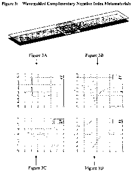
[0015] Figures 3-3D depict a wave-guided structure with both CSRR and CELC
elements (e.g. to provide an effective negative index) (Figure 3) and
associated plots
of effective permittivity, permeability, wave impedance, and refractive index
(Figures
3A-3D);
[0016] Figures 4-4D depict a wave-guided structure with both CSRR and CELC
elements (e.g. to provide an effective negative index) (Figure 4) and
associated plots
of effective permittivity, permeability, wave impedance, and refractive index
(Figures
4A-4D);
CA 02734962 2011-02-22
WO 2010/021736 PCT/US2009/004772
6
[0017] Figures 5-5D depict a microstrip complementary ELC structure (Figure
5) and associated plots of effective permittivity, permeability, wave
impedance, and
refractive index (Figures 5A-5D);
[0018] Figures 6-6D are depict a microstrip structure with both CSRR and
CELC elements (e.g. to provide an effective negative index) (Figure 6) and
associated
plots of effective permittivity, permeability, wave impedance, and refractive
index
(Figures 6A-6D);
[0019] Figure 7 depicts an exemplary CSRR array as a 2D planar waveguide
structure;
[0020] Figure 8-1 depicts retrieved permittivity and permeability of a CSRR
element, and Figure 8-2 depicts the dependence of the retrieved permittivity
and
permeability on a geometrical parameter of the CSRR element;
[0021] Figures 9-1, 9-2 depict field data for 2D implementations of the planar
waveguide structure for beam-steering and beam-focusing applications,
respectively;
[0022] Figures 10-1, 10-2 depict an exemplary CELC array as a 2D planar
waveguide structure providing an indefinite medium; and
[0023] Figures 11-1, 11-2 depict a waveguide based gradient index lens
deployed as a feed structure for an array of patch antennas.
DETAILED DESCRIPTION
[0024] Various embodiments disclosed herein include "complementary"
metamaterial elements, which may be regarded as Babinet complements of
original
metamaterial elements such as split ring resonators (SRRs) and electric LC
resonators (ELCs).
[0025] The SRR element functions as an artificial magnetic dipolar "atom,"
producing a substantially magnetic response to the magnetic field of an
electromagnetic wave. Its Babinet "dual," the complementary split ring
resonator
(CSRR), functions as an electric dipolar "atom" embedded in a conducting
surface and
CA 02734962 2011-02-22
WO 2010/021736 PCT/US2009/004772
7
producing a substantially electric response to the electric field of an
electromagnetic
wave. While specific examples are described herein that deploy CSRR elements
in
various structures, other embodiments may substitute alternative elements. For
example, any substantially planar conducting structure having a substantially
magnetic response to an out-of-plane magnetic field (hereafter referred to as
a "M-
type element," the SRR being an example thereof) may define a complement
structure
(hereafter a "complementary M-type element," the CSRR being an example
thereof),
which is a substantially-equivalently-shaped aperture, etching, void, etc.
within a
conducting surface. The complementary M-type element will have a Babinet-dual
response, i.e. a substantially electric response to an out-of-plane electric
field.
Various M-type elements (each defining a corresponding complementary M-type
element) may include: the aforementioned split ring resonators (including
single split
ring resonators (SSRRs), double split ring resonators (DSRRs), split-ring
resonators
having multiple gaps, etc.), omega-shaped elements (cf. C.R. Simovski and S.
He,
arXiv:physics/0210049), cut-wire-pair elements (cf. G. Dolling et al, Opt.
Left. 30, 3198
(2005)), or any other conducting structures that are substantially
magnetically
polarized (e.g. by Faraday induction) in response to an applied magnetic
field.
[0026] The ELC element functions as an artificial electric dipolar "atom,"
producing a substantially electric response to the electric field of an
electromagnetic
wave. Its Babinet "dual," the complementary electric LC (CELC) element,
functions as
a magnetic dipolar "atom" embedded in a conducting surface and producing a
substantially magnetic response to the magnetic field of an electromagnetic
wave.
While specific examples are described herein that deploy CELC elements in
various
structures, other embodiments may substitute alternative elements. For
example, any
substantially planar conducting structure having a substantially electric
response to an
in-plane electric field (hereafter referred to as a "E-type element," the ELC
element
being an example thereof) may define a complement structure (hereafter a
"complementary E-type element," the CELC being an example thereof), which is a
substantially-equivalently-shaped aperture, etching, void, etc. within a
conducting
surface. The complementary E-type element will have a Babinet-dual response,
i.e. a
substantially magnetic response to an in-plane magnetic field. Various E-type
elements (each defining a corresponding complementary E-type element) may
CA 02734962 2011-02-22
WO 2010/021736 PCT/US2009/004772
8
include: capacitor-like structures coupled to oppositely-oriented loops (as in
Figures 1,
3, 4, 5, 6, and 10-1, with other exemplary varieties depicted in D. Schurig et
al,
"Electric-field-coupled resonators for negative permittivity metamaterials,"
Appl. Phys.
Left. 88, 041109 (2006) and in H.-T. Cen et al, "Complementary planar
terahertz
metamaterials," Opt. Exp. 15, 1084 (2007)), closed-ring elements (cf. R. Liu
et al,
"Broadband gradient index optics based on non-resonant metamaterials,"
unpublished; see attached Appendix), I-shaped or "dog-bone" structures (cf. R.
Liu et
al, "Broadband ground-plane cloak," Science 323, 366 (2009)), cross-shaped
structures (cf. H.-T. Cen et al, previously cited), or any other conducting
structures
that are substantially electrically polarized in response to an applied
electric field. In
various embodiments, a complementary E-type element may have a substantially
isotropic magnetic response to in-plane magnetic fields, or a substantially
anisotropic
magnetic response to in-plane magnetic fields.
[0027] While an M-type element may have a substantial (out-of-plane) magnetic
response, in some approaches an M-type element may additionally have an (in-
plane)
electric response that is also substantial but of lesser magnitude than (e.g.
having a
smaller susceptibility than) the magnetic response. In these approaches, the
corresponding complementary M-type element will have a substantial (out-of-
plane)
electric response, and additionally an (in-plane) magnetic response that is
also
substantial but of lesser magnitude than (e.g. having a smaller susceptibility
than) the
electric response. Similarly, while an E-type element may have a substantial
(in-
plane) electric response, in some approaches an E-type element may
additionally
have an (out-of-plane) magnetic response that is also substantial but of
lesser
magnitude than (e.g. having a smaller susceptibility than) the electric
response. In
these approaches, the corresponding complementary E-type element will have a
substantial (in-plane) magnetic response, and additionally an (out-of-plane)
electric
response that is also substantial but of lesser magnitude than (e.g. having a
smaller
susceptibility than) the magnetic response.
[0028] Some embodiments provide a waveguide structure having one or more
bounding conducting surfaces that embed complementary elements such as those
described previously. In a waveguide context, quantitative assignment of
quantities
CA 02734962 2011-02-22
WO 2010/021736 PCT/US2009/004772
9
typically associated with volumetric materials-such as the electric
permittivity,
magnetic permeability, refractive index, and wave impedance-may be defined for
planar waveguides and microstrip lines patterned with the complementary
structures.
For example, one or more complementary M-type elements such as CSRRs,
patterned in one or more bounding surfaces of a waveguide structure, may be
characterized as having an effective electric permittivity. Of note, the
effective
permittivity can exhibit both large positive and negative values, as well as
values
between zero and unity, inclusive. Devices can be developed based at least
partially
on the range of properties exhibited by the M-type elements, as will be
described.
The numerical and experimental techniques to quantitatively make this
assignment
are well-characterized.
[0029] Alternatively or additionally, in some embodiments complementary E-
type elements such as CELCs, patterned into a waveguide structure in the same
manner as described above, have a magnetic response that may be characterized
as
an effective magnetic permeability. The complementary E-type elements thus can
exhibit both large positive and negative values of the effective permeability,
as well as
effective permeabilities that vary between zero and unity, inclusive.
(throughout this
disclosure, real parts are generally referred to in the descriptions of the
permittivity
and permeability for both the complementary E-type and complementary M-type
structures, except where context dictates otherwise as shall be apparent to
one of skill
in the art) Because both types of resonators can be implemented in the
waveguide
context, virtually any effective material condition can be achieved, including
negative
refractive index (both permittivity and permeability less than zero), allowing
considerable control over waves propagating through these structures. For
example,
some embodiments may provide effective constitutive parameters substantially
corresponding to a transformation optical medium (as according to the method
of
transformation optics, e.g. as described in J. Pendry et al, "Electromagnetic
cloaking
method," U.S. Patent App. No. 11/459728).
[0030] Using a variety of combinations of the complementary E- and/or M-type
elements, a wide variety of devices can be formed. For example, virtually all
of the
devices that have been demonstrated by Caloz and Itoh using CRLH TLs have
CA 02734962 2011-02-22
WO 2010/021736 PCT/US2009/004772
analogs in the waveguiding metamaterial structures described here. Most
recently,
Silvereinha and Engheta proposed an interesting coupler based on creating a
region
in which the effective refractive index (or propagation constant) is nearly
zero (CITE).
The equivalent of such a medium can be created by the patterning of
complementary
5 E- and/or M-type elements into the bounding surfaces of a waveguide
structure. The
Figures show and describe exemplary illustrative non-limiting realizations of
the zero
index coupler and other devices with the use of patterned waveguides and
several
depictions as to how exemplary non-limiting structures may be implemented.
[0031] Figure 1 shows an exemplary illustrative non-limiting wave-guided
10 complementary ELC (magnetic response) structure, and Figures 1A-1D show
associated exemplary plots of the effective index, wave impedance,
permittivity and
permeability. While the depicted example shows only a single CELC element,
other
approaches provide a plurality of CELC (or other complementary E-type)
elements
disposed on one or more surfaces of a waveguide structure.
[0032] Figure 2 shows an exemplary illustrative non-limiting wave-guided
complementary SRR (electric response) structure, and Figures 2A-2D show
associated exemplary plots of the effective index, wave impedance,
permittivity and
permeability. While the depicted example shows only a single CSRR element,
other
approaches provide a plurality of CSRR elements (or other complementary M-
type)
elements disposed on one or more surfaces of a waveguide structure.
[0033] Figure 3 shows an exemplary illustrative non-limiting wave-guided
structure with both CSRR and CELC elements (e.g. to provide an effective
negative
index) in which the CSRR and CELC are patterned on opposite surfaces of a
planar
waveguide, and Figures 3A-3D show associated exemplary plots of the effective
index, wave impedance, permittivity and permeability. While the depicted
example
shows only a single CELC element on a first bounding surface of a waveguide
and a
single CSRR element on a second bounding surface of the waveguide, other
approaches provide a plurality of complementary E- and/or M-type elements
disposed
on one or more surfaces of a waveguide structure.
CA 02734962 2011-02-22
WO 2010/021736 PCT/US2009/004772
11
[0034] Figure 4 shows an exemplary illustrative non-limiting wave-guided
structure with both CSRR and CELC elements (e.g. to provide an effective
negative
index) in which the CSRR and CELC are patterned on the same surface of a
planar
waveguide, and Figures 4A-4D show associated exemplary plots of the effective
index, wave impedance, permittivity and permeability. While the depicted
example
shows only a single CELC element and a single CSRR element on a first bounding
surface of a waveguide, other approaches provide a plurality of complementary
E-
and/or M-type elements disposed on one or more surfaces of a waveguide
structure.
[0035] Figure 5 shows an exemplary illustrative non-limiting microstrip
complementary ELC structure, and Figures 5A-5D show associated exemplary plots
of the effective index, wave impedance, permittivity and permeability. While
the
depicted example shows only a single CELC element on the ground plane of a
microstrip structure, other approaches provide a plurality of CELC (or other
complementary E-type) elements disposed on one or both of the strip portion of
the
microstrip structure or the ground plane portion of the microstrip structure.
[0036] Figure 6 shows an exemplary illustrative non-limiting micro-strip line
structure with both CSRR and CELC elements (e.g. to provide an effective
negative
index), and Figures 6A-6D show associated exemplary plots of the effective
index,
wave impedance, permittivity and permeability. While the depicted example
shows
only a single CSRR element and two CELC elements on the ground plane of a
microstrip structure, other approaches provide a plurality of complementary E-
and/or
M-type elements disposed on one or both of the strip portion of the microstrip
structure or the ground plane portion of the microstrip structure.
[0037] Figure 7 illustrates the use of a CSRR array as a 2D waveguide
structure. In some approaches a 2D waveguide structure may have bounding
surfaces (e.g. the upper and lower metal places depicted in Figure 7) that are
patterned with complementary E- and/or M-type elements to implement
functionality
such as impedance matching, gradient engineering, or dispersion control.
[0038] As an example of gradient engineering, the CSRR structure of Figure
7has been utilized to form both gradient index beam-steering and beam-focusing
CA 02734962 2011-02-22
WO 2010/021736 PCT/US2009/004772
12
structures. Figure 8-1 illustrates a single exemplary CSRR and the retrieved
permittivity and permeability corresponding to the CSRR (in the waveguide
geometry).
By changing parameters within the CSRR design (in this case a curvature of
each
bend of the CSRR), the index and/or the impedance can be tuned, as shown in
Figure
8-2.
[0039] A CSRR structure laid out as shown in Figure 7, with a substantially
linear gradient of refractive index imposed along the direction transverse to
the
incident guided beam, produces an exit beam that is steered to an angle
different from
that of the incident beam. Figure 9-1 shows exemplary field data taken on a 2D
implementation of the planar waveguide beam-steering structure. The field
mapping
apparatus has been described in considerable detail in the literature [B. J.
Justice, J.
J. Mock, L. Guo, A. Degiron, D. Schurig, D. R. Smith, "Spatial mapping of the
internal
and external electromagnetic fields of negative index metamaterials," Optics
Express,
vol. 14, p. 8694 (2006)]. Likewise, implementing a parabolic refractive index
gradient
along the direction transverse to the incident beam within the CSRR array
produces a
focusing lens, e.g. as shown in Figure 9-2. More generally, a transverse index
profile
that is a concave function (parabolic or otherwise) will provide a positive
focusing
effect, such as depicted in Figure 9-2 (corresponding to a positive focal
length); a
transverse index profile that is a convex function (parabolic or otherwise)
will provide a
negative focusing effect (corresponding to a negative focal length, e.g. to
receive a
collimated beam and transmit a diverging beam). For approaches wherein the
metamaterial elements include adjustable metamaterial elements (as discussed
below), embodiments may provide an apparatus having an electromagnetic
function
(e.g. beam steering, beam focusing, etc.) that is correspondingly adjustable.
Thus, for
example, a beam steering apparatus may be adjusted to provide at least first
and
second deflection angles; a beam focusing apparatus may be adjusted to provide
at
least first and second focal lengths, etc. An example of a 2D medium formed
with
CELCs is shown in Figures 10-1, 10-2. Here, an in-plane anisotropy of the
CELCs is
used to form an 'indefinite medium,' in which a first in-plane component of
the
permeability is negative while another in-plane component is positive. Such a
medium produces a partial refocusing of waves from a line source, as shown in
the
experimentally obtained field map of Figure 10-2. The focusing properties of a
bulk
CA 02734962 2011-02-22
WO 2010/021736 PCT/US2009/004772
13
indefinite medium have previously been reported [D. R. Smith, D. Schurig, J.
J. Mock,
P. Kolinko, P. Rye, "Partial focusing of radiation by a slab of indefinite
media," Applied
Physics Letters, vol. 84, p. 2244 (2004)]. The experiments shown in this set
of figures
validate the design approach, and show that waveguide metamaterial elements
can
be produced with sophisticated functionality, including anisotropy and
gradients.
[0040] In Figures 11-1 and 11-2, a waveguide-based gradient index structure
(e.g. having boundary conductors that include complementary E- and/or M-type
elements, as in Figures 7 and 10-1) is disposed as a feed structure for an
array of
patch antennas. In the exemplary embodiment of Figures 11-1 and 11-2, the feed
structure collimates waves from a single source that then drive an array of
patch
antennas. This type of antenna configuration is well known as the Rotman lens
configuration. In this exemplary embodiment, the waveguide metamaterial
provides an
effective gradient index lens within a planar waveguide, by which a plane wave
can be
generated by a point source positioned on the focal plane of the gradient
index lens,
as illustrated by the "feeding points" in Figure 11-2. For the Rotman Lens
antenna,
one can place multiple feeding points on the focal plane of the gradient index
metamaterial lens and connect antenna elements to the output of the waveguide
structure as shown in Figure 11-1. From well known optics theory, the phase
difference between each antenna will depend on the feed position of the
source, so
that phased-array beam forming can be implemented. Figure 11-2 is a field map,
showing the fields from a line source driving the gradient index planar
waveguide
metamaterial at the focus, resulting in a collimated beam. While the exemplary
feed
structure of Figures 11-1 and 11-2 depicts a Rotman-lens type configuration
for which
the antenna phase differences are substantially determined by the location of
the
feeding point, in other approaches the antenna phase differences are
determined by
fixing the feeding point and adjusting the electromagnetic properties (and
therefore the
phase propagation characteristics of) the gradient index lens (e.g. by
deploying
adjustable metamaterial elements, as discussed below), while other embodiments
may combine both approaches (i.e. adjustment of both the feeding point
position and
the lens parameters to cumulatively achieve the desired antenna phase
differences).
CA 02734962 2011-02-22
WO 2010/021736 PCT/US2009/004772
14
[0041] In some approaches, a waveguide structure having an input port or
input region for receiving electromagnetic energy may include an impedance
matching
layer (IML) positioned at the input port or input region, e.g. to improve the
input
insertion loss by reducing or substantially eliminating reflections at the
input port or
input region. Alternatively or additionally, in some approaches a waveguide
structure
having an output port or output region for transmitting electromagnetic energy
may
include an impedance matching layer (IML) positioned at the output port or
output
region, e.g. to improve the output insertion loss by reducing or substantially
eliminating reflections at the output port or output region. An impedance
matching
layer may have a wave impedance profile that provides a substantially
continuous
variation of wave impedance, from an initial wave impedance at an external
surface of
the waveguide structure (e.g. where the waveguide structure abuts an adjacent
medium or device) to a final wave impedance at an interface between the IML
and a
gradient index region (e.g. that provides a device function such as beam
steering or
beam focusing). In some approaches the substantially continuous variation of
wave
impedance corresponds to a substantially continuous variation of refractive
index (e.g.
where turning an arrangement of one species of element adjusts both an
effective
refractive and an effective wave impedance according to a fixed
correspondence,
such as depicted in Figure 8-2), while in other approaches the wave impedance
may
be varied substantially independently of the refractive index (e.g. by
deploying both
complementary E- and M-type elements and independently turning the
arrangements
of the two species of elements to correspondingly independently tune the
effective
refractive index and the effective wave impedance).
[0042] While exemplary embodiments provide spatial arrangements of
complementary metamaterial elements having varied geometrical parameters (such
as a length, thickness, curvature radius, or unit cell dimension) and
correspondingly
varied individual electromagnetic responses (e.g. as depicted in Figure 8-2),
in other
embodiments other physical parameters of the complementary metamaterial
elements
are varied (alternatively or additionally to varying the geometrical
parameters) to
provide the varied individual electromagnetic responses. For example,
embodiments
may include complementary metamaterial elements (such as CSRRs or CELCs) that
are the complements of original metamaterial elements that include capacitive
gaps,
CA 02734962 2011-02-22
WO 2010/021736 PCT/US2009/004772
and the complementary metamaterial elements may be parameterized by varied
capacitances of the capacitive gaps of the original metamaterial elements.
Equivalently, noting that from Babinet's theorem a capacitance in an element
(e.g. in
the form of a planar interdigitated capacitor having a varied number of digits
and/or
5 varied digit length) becomes an inductance in the complement thereof (e.g.
in the form
of a meander line inductor having a varied number of turns and/or varied turn
length),
the complementary elements may be parameterized by varied inductances of the
complementary metamaterial elements. Alternatively or additionally,
embodiments
may include complementary metamaterial elements (such as CSRRs or CELCs) that
10 are the complements of original metamaterial elements that include
inductive circuits,
and the complementary metamaterial elements may be parameterized by varied
inductances of the inductive circuits of the original metamaterial elements.
Equivalently, noting that from Babinet's theorem an inductance in an element
(e.g. in
the form of a meander line inductor having a varied number of turns and/or
varied turn
15 length) becomes a capacitance in the complement thereof (e.g. in the form
of an
planar interdigitated capacitor having a varied number of digits and/or varied
digit
length), the complementary elements may be parameterized by varied
capacitances
of the complementary metamaterial elements. Moreover, a substantially planar
metamaterial element may have its capacitance and/or inductance augmented by
the
attachment of a lumped capacitor or inductor. In some approaches, the varied
physical parameters (such as geometrical parameters, capacitances,
inductances) are
determined according to a regression analysis relating electromagnetic
responses to
the varied physical parameters (c.f. the regression curves in Figure 8-2)
[0043] In some embodiments the complementary metamaterial elements are
adjustable elements, having adjustable physical parameters corresponding to
adjustable individual electromagnetic responses of the elements. For example,
embodiments may include complementary elements (such as CSRRs) having
adjustable capacitances (e.g. by adding varactor diodes between the internal
and
external metallic regions of the CSRRs, as in A. Velez and J. Bonarche,
"Varactor-
loaded complementary split ring resonators (VLCSRR) and their application to
tunable
metamaterial transmission lines," IEEE Microw. Wireless Compon. Lett. 18, 28
(2008)). In another approach, for waveguide embodiments having an upper and a
CA 02734962 2011-02-22
WO 2010/021736 PCT/US2009/004772
16
lower conductor (e.g. a strip and a ground plane) with an intervening
dielectric
substrate, complementary metamaterial elements embedded in the upper and/or
lower conductor may be adjustable by providing a dielectric substrate having a
nonlinear dielectric response (e.g. a ferroelectric material) and applying a
bias voltage
between the two conductors. In yet another approach, a photosensitive material
(e.g.
a semiconductor material such as GaAs or n-type silicon) may be positioned
adjacent
to a complementary metamaterial element, and the electromagnetic response of
the
element may be adjustable by selectively applying optical energy to the
photosensitive
material (e.g. to cause photodoping). In yet another approach, a magnetic
layer (e.g.
of a ferrimagnetic or ferromagnetic material) may be positioned adjacent to a
complementary metamaterial element, and the electromagnetic response of the
element may be adjustable by applying a bias magnetic field (e.g. as described
in J.
Gollub et al, "Hybrid resonant phenomenon in a metamaterial structure with
integrated
resonant magnetic material," arXiv:0810.4871 (2008)). While exemplary
embodiments herein may employ a regression analysis relating electromagnetic
responses to geometrical parameters (cf. the regression curve in Figure 8-2),
embodiments with adjustable elements may employ a regression analysis relating
electromagnetic responses to adjustable physical parameters that substantially
correlate with the electromagnetic responses.
[0044] In some embodiments with adjustable elements having adjustable
physical parameters, the adjustable physical parameters may be adjustable in
response to one or more external inputs, such as voltage inputs (e.g. bias
voltages for
active elements), current inputs (e.g. direct injection of charge carriers
into active
elements), optical inputs (e.g. illumination of a photoactive material), or
field inputs
(e.g. bias electric/magnetic fields for approaches that include
ferroelectrics/ferromagnets). Accordingly, some embodiments provide methods
that
include determining respective values of adjustable physical parameters (e.g.
by a
regression analysis), then providing one or more control inputs corresponding
to the
determined respective values. Other embodiments provide adaptive or adjustable
systems that incorporate a control unit having circuitry configured to
determine
respective values of adjustable physical parameters (e.g. by a regression
analysis)
CA 02734962 2011-02-22
WO 2010/021736 PCT/US2009/004772
17
and/or provide one or more control inputs corresponding to determined
respective
values.
[0045] While some embodiments employ a regression analysis relating
electromagnetic responses to physical parameters (including adjustable
physical
parameters), for embodiments wherein the respective adjustable physical
parameters
are determined by one or more control inputs, a regression analysis may
directly
relate the electromagnetic responses to the control inputs. For example, where
the
adjustable physical parameter is an adjustable capacitance of a varactor diode
as
determined from an applied bias voltage, a regression analysis may relate
electromagnetic responses to the adjustable capacitance, or a regression
analysis
may relate electromagnetic responses to the applied bias voltage.
[0046] While some embodiments provide substantially narrow-band responses
to electromagnetic radiation (e.g. for frequencies in a vicinity of one or
more
resonance frequencies of the complementary metamaterial elements), other
embodiments provide substantially broad-band responses to electromagnetic
radiation
(e.g. for frequencies substantially less than, substantially greater than, or
otherwise
substantially different than one or more resonance frequencies of the
complementary
metamaterial elements). For example, embodiments may deploy the Babinet
complements of broadband metamaterial elements such as those described in R.
Liu
et al, "Broadband gradient index optics based on non-resonant meta materia
Is,"
unpublished; see attached Appendix) and/or in R. Liu et al, "Broadband ground-
plane
cloak," Science 323, 366 (2009)).
[0047] While the preceding exemplary embodiments are planar embodiments
that are substantially two-dimensional, other embodiments may deploy
complementary metamaterial elements in substantially non-planar
configurations,
and/or in substantially three-dimensional configurations. For example,
embodiments
may provide a substantially three-dimensional stack of layers, each layer
having a
conducting surface with embedded complementary metamaterial elements.
Alternatively or additionally, the complementary metamaterial elements may be
embedded in conducting surfaces that are substantially non-planar (e.g.
cylinders,
spheres, etc.). For example, an apparatus may include a curved conducting
surface
CA 02734962 2011-02-22
WO 2010/021736 PCT/US2009/004772
18
(or a plurality thereof) that embeds complementary metamaterial elements, and
the
curved conducting surface may have a radius of curvature that is substantially
larger
than a typical length scale of the complementary metamaterial elements but
comparable to or substantially smaller than a wavelength corresponding to an
operating frequency of the apparatus.
[0048] While the technology herein has been described in connection with
exemplary illustrative non-limiting implementations, the invention is not to
be limited by
the disclosure. The invention is intended to be defined by the claims and to
cover all
corresponding and equivalent arrangements whether or not specifically
disclosed
herein.
[0049] All documents and other information sources cited above are hereby
incorporated in their entirety by reference.