Note : Les descriptions sont présentées dans la langue officielle dans laquelle elles ont été soumises.
CA 02738099 2011-04-20
DIELECTRIC COMPOSITION FOR THIN-FILM TRANSISTORS
BACKGROUND
[0001] The present disclosure relates, in various embodiments, to thin-film
transistors (TFTs) and/or other electronic devices comprising a gate
dielectric layer.
The gate dielectric layer is formed from a dielectric composition as described
herein
that contains an infrared (IR) absorber or IR absorbing agent. This allows the
dielectric composition to be selectively cured while its substrate remains at
a
relatively lower temperature, preventing deformation of the substrate.
[0002] TFTs are generally composed of, on a substrate, an electrically
conductive
gate electrode, source and drain electrodes, an electrically insulating gate
dielectric
layer which separate the gate electrode from the source and drain electrodes,
and a
semiconducting layer which is in contact with the gate dielectric layer and
bridges
the source and drain electrodes. Their performance can be determined by the
field
effect mobility and the current on/off ratio of the overall transistor. High
mobility and
high on/off ratio are desired.
[0003] There is interest in organic thin-film transistors (OTFTs) for
applications
such as radio frequency identification (RFID) tags and backplane switching
circuits
for displays, such as signage, readers, and liquid crystal displays, where
high
switching speeds and/or high density are not essential. OTFTs may be made
using
low-cost solution or liquid fabrication techniques. They also have attractive
mechanical properties such as being physically compact, lightweight, and
flexible.
[0004] Recently, there has been an increased interest in organic thin-film
transistors which can potentially be fabricated using solution-based
patterning and
deposition techniques, such as spin coating, solution casting, dip coating,
stencil/screen printing, flexography, gravure, offset printing, ink jet-
printing, micro-
contact printing, and the like, or a combination of these processes. Such
processes
are generally simpler and more cost effective compared to the complex
photolithographic processes used in fabricating silicon-based thin-film
transistor
circuits for electronic devices. To enable the use of these solution-based
processes
in fabricating thin-film transistor circuits, solution processable materials
are therefore
required.
- 1 -
CA 02738099 2011-04-20
[0005] In this regard, gate dielectric layers may be formed by these
solution-
based processes. However, the gate dielectric layer so formed should be free
of
pinholes and possess low surface roughness (or high surface smoothness), low
leakage current, a high dielectric constant, a high breakdown voltage, adhere
well to
the gate electrode, be stable in solution at room temperature, and offer other
functionality. It should also be compatible with semiconductor materials
because the
interface between the dielectric layer and the organic semiconductor layer
critically
affects the performance of the TFT.
[0006] Roll-to-roll manufacturing refers to the process, still somewhat in
development, of creating electronic devices on a roll of flexible plastic or
metal foil,
similar to the gravure, offset, and flexographic printing processes used with
paper. It
is contemplated that large circuits made with thin-film transistors and other
devices
can be easily patterned onto these large substrates, which can be up to a few
metres wide and 50 km long. This type of manufacturing would allow for large-
scale
low-cost devices, especially when compared to normal semiconductor
manufacturing processes that use photolithography techniques.
[0007] Low temperatures and increased speed of processing are critical to
roll-to-
roll manufacturing. In this regard, a solution processable dielectric layer is
generally
applied as a solution and then cured. The thermal curing generally occurs at a
temperature, for example, from about 140 C to 180 C and for a period, for
example,
from 10 minutes to 30 minutes, to ensure optimal performance of the resulting
composition. These curing temperatures and times are, in most cases, not
compatible with roll-to-roll manufacturing.
[0008] It would be desirable to provide a dielectric layer and/or
dielectric
composition that could be processed at lower temperatures and/or shorter time
periods, to allow for manufacture of an electronic device using roll-to-roll
manufacturing and other processes.
BRIEF DESCRIPTION
[0009] Disclosed in embodiments are electronic devices and processes for
making such electronic devices. Generally, the dielectric layer is formed from
a
- 2 -
CA 02738099 2011-04-20
dielectric composition as described herein that contains an infrared (IR)
absorber or
IR absorbing agent. During the curing process, this composition allows the
dielectric
composition to attain higher temperatures than the other components of the
electronic device, particularly the substrate. This reduces deformation of the
substrate. The electronic device comprises a dielectric layer, and the
dielectric layer
comprises a crosslinking dielectric material and an infrared absorber. In
embodiments, the electronic devices are thin film transistors, particularly
thin film
transistors on a flexible substrate, such as low-cost polyethylene
terephthalate
(PET).
[0010] Described in some embodiments is a process for fabricating an
electronic
device. A dielectric composition is deposited on a substrate. The dielectric
composition comprises a dielectric material, a crosslinking agent, and an
infrared
absorbing agent. The dielectric composition is then exposed to infrared
radiation to
cure the dielectric composition, forming a dielectric layer on the substrate.
A
semiconductor layer is then formed on the substrate.
[0011] The dielectric material may comprise a lower-k dielectric material
and a
higher-k dielectric material. The lower-k dielectric material has a dielectric
constant
of less than 4Ø The higher-k dielectric material has a dielectric constant
of 4.0 or
higher. In some embodiments, the lower-k dielectric material is a lower-k
polymer. In
other embodiments, the higher-k dielectric material is a higher-k polymer. In
specific
embodiments, the lower-k dielectric polymer is poly(methyl silsesquioxane) and
the
higher-k dielectric polymer is poly(4-vinyl phenol). The exposure to infrared
radiation
can cause the higher-k dielectric material and the lower-k dielectric material
to
separate into two phases, the lower-k dielectric material being in a higher
concentration than the higher-k dielectric material in the phase of the
dielectric layer
closest to the semiconductor layer.
[0012] The infrared absorbing agent may have an absorption maximum of from
about 800 nm to about 1200 nm. The infrared absorbing agent may be present in
the amount of from about 0.001 to about 5 wt% of the dielectric layer when
cured.
[0013] The dielectric composition can be exposed to infrared radiation
using a
laser. In embodiments, the infrared absorbing agent has an absorption maximum
of
- 3 -
CA 02738099 2014-10-08
from about 800 nm to about 1200 nm, and the laser emits at a wavelength
which is within 5% of the absorption maximum of the infrared absorbing
agent.
[0014] The dielectric composition may also be heated with a heat source
separate from the device that delivers the infrared radiation. The heat
source is in particular embodiments a hotplate or an oven.
[0015] The dielectric composition can be exposed to infrared radiation for
a
period of from about lsecond to about 30 minutes.
[0016] During curing, the substrate attains a temperature of from about
room
temperature to about 160 C, particularly from about room temperature to about
120 C, and the dielectric composition attains a higher temperature than the
substrate. The difference between the temperature of the dielectric
composition
and the temperature of the substrate may be at least 20 C.
[0017] Also disclosed in embodiments is a dielectric composition comprising
a
dielectric material, a crosslinking agent, and an infrared absorbing agent.
The
dielectric material may comprise a lower-k dielectric material and a higher-k
dielectric material, and the dielectric composition may further comprise a
liquid in
which both the lower-k dielectric material and the higher-k dielectric
material are
miscible.
[0018] The lower-k dielectric material may be poly(methyl silsesquioxane).
The higher-k dielectric material may be poly(4-vinyl phenol).
[0019] The infrared absorbing agent may have an absorption maximum of
from about 800 nm to about 1200 nm, and the infrared absorbing agent may be
present in the amount of from about 0.001 to about 5 wt%, based on the weight
of the dielectric composition.
[0019a] In accordance with an aspect of the present invention there is
provided
a process for fabricating an electronic device, comprising: depositing a
dielectric
composition on a substrate, the dielectric composition comprising a dielectric
material, a crosslinking agent, and an infrared absorbing agent; exposing the
dielectric composition to infrared radiation to cure the dielectric
composition,
forming a dielectric layer on the substrate; and forming a semiconductor layer
on
the substrate.
[0019b] In accordance with a further aspect of the present invention there is
provided an electronic device comprising a dielectric layer, the dielectric
layer
comprising a crosslinked dielectric material and an infrared absorbing agent.
- 4 -
CA 02738099 2013-01-11
[0019c] In accordance with a further aspect of the present invention there is
provided a dielectric composition comprising a dielectric material, a
crosslinking
agent, and an infrared absorbing agent.
[0020] These and other non-limiting characteristics of the disclosure are
more
particularly disclosed below.
BRIEF DESCRIPTION OF THE DRAWINGS
[0021] The following is a brief description of the drawings, which are
presented for the purposes of illustrating the exemplary embodiments disclosed
herein and not for the purposes of limiting the same.
- 4a -
CA 02738099 2011-04-20
I ,
[0022]
FIG. 1 represents a first embodiment of a TFT according to the present
disclosure.
[0023]
FIG. 2 represents a second embodiment of a TFT according to the present
disclosure.
[0024]
FIG. 3 represents a third embodiment of a TFT according to the present
disclosure.
[0025]
FIG. 4 represents a fourth embodiment of a TFT according to the present
disclosure.
DETAILED DESCRIPTION
[0026] A more complete understanding of the components, processes and
apparatuses disclosed herein can be obtained by reference to the accompanying
drawings.
These figures are merely schematic representations based on
convenience and the ease of demonstrating the present disclosure, and are,
therefore, not intended to indicate relative size and dimensions of the
devices or
components thereof and/or to define or limit the scope of the exemplary
embodiments.
[0027]
Although specific terms are used in the following description for the
sake
of clarity, these terms are intended to refer only to the particular structure
of the
embodiments selected for illustration in the drawings, and are not intended to
define
or limit the scope of the disclosure. In the drawings and the following
description
below, it is to be understood that like numeric designations refer to
components of
like function.
[0028]
The modifier "about" used in connection with a quantity is inclusive of
the
stated value and has the meaning dictated by the context (for example, it
includes at
least the degree of error associated with the measurement of the particular
quantity).
When used in the context of a range, the modifier "about" should also be
considered
as disclosing the range defined by the absolute values of the two endpoints.
For
example, the range of "from about 2 to about 10" also discloses the range
"from 2 to
10."
- 5 -
CA 02738099 2011-04-20
[0029] The
term "room temperature" refers to a temperature of from 20 C to
25 C.
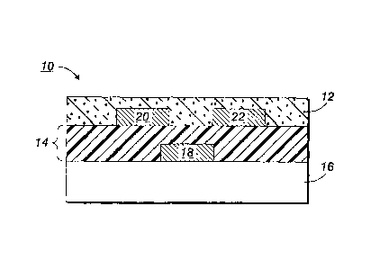
[0030] FIG. 1 illustrates a bottom-gate bottom-contact TFT configuration
according to the present disclosure. The TFT 10 comprises a substrate 16 in
contact with the gate electrode 18 and a gate dielectric layer 14. Although
here the
gate electrode 18 is depicted atop the substrate 16, but could also be located
within
the substrate. It is important that the gate dielectric layer 14 separates the
gate
electrode 18 from the source electrode 20, drain electrode 22, and the
semiconducting layer 12. The semiconducting layer 12 runs over and between the
source and drain electrodes 20 and 22. The semiconductor has a channel length
between the source and drain electrodes 20 and 22.
[0031] FIG. 2
illustrates another bottom-gate top-contact TFT configuration
according to the present disclosure. The TFT 30 comprises a substrate 36 in
contact with the gate electrode 38 and a gate dielectric layer 34. The
semiconducting layer 32 is placed on top of the gate dielectric layer 34 and
separates it from the source and drain electrodes 40 and 42.
[0032] FIG. 3 illustrates a bottom-gate bottom-contact TFT configuration
according to the present disclosure. The TFT 50 comprises a substrate 56 which
also acts as the gate electrode and is in contact with a gate dielectric layer
54. The
source electrode 60, drain electrode 62, and semiconducting layer 52 are
located
atop the gate dielectric layer 54.
[0033] FIG. 4
illustrates a top-gate top-contact TFT configuration according to the
present disclosure. The TFT 70 comprises a substrate 76 in contact with the
source
electrode 80, drain electrode 82, and the semiconducting layer 72. The
semiconducting layer 72 runs over and between the source and drain electrodes
80
and 82. The gate dielectric layer 74 is on top of the semiconducting layer 72.
The
gate electrode 78 is on top of the gate dielectric layer 74 and does not
contact the
semiconducting layer 72.
[0034]
Aspects of the present disclosure relate to an electronic device (e.g., a
thin-film transistor) comprising a dielectric layer, the dielectric layer
comprising an
infrared absorber. In some embodiment, the dielectric layer is a single
homogeneous
- 6 -
CA 02738099 2011-04-20
layer, or in other words is not composed of multiple phase-separated
materials.
Further aspects of the present disclosure relate to an electronic device
comprising a
phase-separated dielectric structure, the dielectric structure comprising an
infrared
absorber. In the context of a thin-film transistor, the phase-separated
dielectric
structure can also be referred to as a "gate dielectric." The phase-separated
dielectric structure can be used in any suitable electronic device. Besides a
thin-film
transistor, other types of suitable electronic devices include, for example,
an
embedded capacitor and an electroluminescent lamp.
[0035] In fabricating the present dielectric structure, a dielectric
composition is
prepared which comprises a dielectric material, a crosslinking agent, an
infrared
absorbing agent, and optionally a solvent or a liquid. In embodiments, any
suitable
insulating material can be used as the dielectric material. In further
embodiments,
the dielectric material is a thermally crosslinkable dielectric material. The
term
"thermally crosslinkable" refers to the fact that the dielectric material
includes
functional groups that can react with an additional crosslinking agent or with
other
functional groups in the dielectric material itself to form a crosslinked
network upon
heating. The dielectric material can comprise two or more different materials
having
different dielectric constants. For example, the dielectric material can
comprise a
lower-k dielectric material and a higher-k dielectric material.
[0036] The terms "lower-k dielectric" and "higher-k dielectric" are used to
differentiate two types of material (based on the dielectric constant) in the
dielectric
composition and in the phase-separated dielectric structure.
[0037] In embodiments, the lower-k dielectric material is electrically
insulating
and is compatible or has good compatibility with a semiconductor layer in the
device.
The terms "compatible" and "compatibility" refer to how well the semiconductor
layer
performs electrically when it is adjacent to or contacting a surface rich in
the lower-k
dielectric polymer.
[0038] In embodiments, the lower-k dielectric material has a hydrophobic
surface
and therefore may exhibit satisfactory to excellent compatibility with
polythiophene
semiconducting polymers. In embodiments, the lower-k dielectric material has a
dielectric constant (permittivity) of for instance less than 4.0, or less than
about 3.5,
- 7 -
CA 02738099 2011-04-20
or particularly less than about 3Ø The lower-k dielectric material may have
non-
polar or weak polar groups such as a methyl group, phenylene group, ethylene
group, Si--C, Si--0--Si, and the like. In embodiments, the lower-k dielectric
material
is a polymer. Representative lower-k dielectric polymers include but are not
limited
to homopolymers such as polystyrene, poly(4-methylstyrene),
poly(chlorostyrene),
poly(a-methylstyrene), polysiloxane such as poly(dimethyl siloxane) and
poly(diphenyl siloxane), polysilsesquioxane such as poly(ethyl
silsesquioxane),
poly(methyl silsesquioxane), and poly(phenyl silsesquioxane), polyphenylene,
poly(1,3-butadiene), poly(.alpha.-vinylnaphtalene), polypropylene,
polyisoprene,
polyisobutylene, polyethylene, poly(4-methyl-1-pentene), poly(p-
xylene),
poly(cyclohexyl methacrylate), poly (propylmethacryIPOSS-co-
methylmethacrylate),
poly(propylmethacryIPOSS-co-styrene), poly(styryIPOSS-co-styrene), poly(vinyl
cinnamate), and the like. In specific embodiments, the lower-k dielectric
polymer is
a polysilsesquioxane, particularly poly(nriethyl silsesquioxane). The
dielectric
constant is measured at room temperature and at 1 kHz frequency. In other
embodiments, the lower-k dielectric material is a molecular compound such as a
molecular glass compound.
[0039] In
embodiments, the surface of the lower-k dielectric polymer, when cast
as a film, has a low surface energy. To characterize the surface energy,
advancing
water contact angle can be used. A high contact angle indicates a low surface
energy. In embodiments, the contact angle is 80 degrees or higher, or higher
than
about 90 degrees, or particularly higher than about 95 degrees.
[0040] In
embodiments, the higher-k dielectric material is electrically insulating
and contains polar groups such as a hydroxyl group, amino group, cyano group,
nitro group, C=0 group, and the like. In embodiments, the higher-k dielectric
material
has a dielectric constant of 4.0 or more, 5.0 or more, or particularly 6.0 or
more. In
embodiments, the higher-k dielectric material is a polymer. General types of
higher-k
dielectric polymers may include polyimide, polyester, polyether, polyacrylate,
polyvinyl, polyketone, and polysulfone. Specific representative higher-k
dielectric
polymers include but are not limited to homopolymers such as poly(4-vinyl
phenol)
(PVP), poly(vinyl alcohol), and poly(2-hydroxylethyl methacrylate) (PHEMA),
- 8 -
CA 02738099 2011-04-20
cyanoethylated poly(vinyl alcohol) (PVA), cyanoethylated cellulose,
poly(vinylidene
fluoride) (PVDF), poly(vinyl pyridine), copolymers thereof, and the like. In
embodiments, the higher-k dielectric material is PVP, PVA, or PHEMA. In other
embodiments, the higher-k dielectric material is a molecular compound such as
a
molecular glass compound.
[0041] In embodiments, the higher-k dielectric polymer, when cast as a
film, has
a high surface energy. In terms of advancing water contact angle, the angle is
for
instance lower than 80 degrees, or lower than about 60 degrees, or lower than
about
50 degrees.
[0042] In embodiments, the difference in magnitude of the dielectric
constant of
the higher-k dielectric material versus the lower-k dielectric material is at
least about
0.5, or at least about 1.0, or at least about 2.0, for example from about 0.5
to about
200.
[0043] In embodiments, the present phase-separated dielectric structure
contains
intentionally created pores (also referred to as voids and apertures) such as
those
created using processes and materials similar to those described in for
example
Lopatin et al., U.S. Pat. No. 6,528,409; Foster et al., U.S. Pat. No.
6,706,464; and
Carter et at., U.S. Pat. No. 5,883,219. In other embodiments, the present
phase-
separated dielectric structure does not contain such intentionally created
pores (but
pinholes may be present in certain embodiments which are not intentionally
created
but rather are an undesired byproduct of the present process). The pinhole
density
in embodiments is for example less than 50 per mm2 (square millimeter), or
less
than 10 per mm2, or less than 5 mm2. In further embodiments, the present phase-
separated dielectric structure is pinhole free. In embodiments, the dielectric
composition is non-photoimageable. In embodiments, there is absent a step to
create pores in the dielectric structure.
[0044] In embodiments, the dielectric structure has an overall dielectric
constant
of more than about 4.0, or more than about 5.0, particularly more than about
6Ø
The overall dielectric constant can be characterized with a metal/dielectric
structure/metal capacitor. Particularly for thin-film transistor applications,
a high
- 9 -
CA 02738099 2011-04-20
overall dielectric constant is desirable in embodiments, so that the device
can be
operated at a relatively low voltage.
[0045] A
crosslinking agent is present in the dielectric composition. When the
dielectric composition comprises two or more materials, such as a higher-k
dielectric
material and a lower-k dielectric material which can separate into two or more
phases during curing, the crosslinking agent causes crosslinking to occur
between
the higher-k dielectric material and the lower-k dielectric material
throughout the
phases. Other
materials can be added into the dielectric composition.
Representative crosslinking agents include poly(melamine-co-formaldehyde)
resin,
oxazoline functional crosslinking agents, blocked polyisocyanates, certain
diamine
compounds, dithiol compounds, diisocyanates, and the like. A catalyst for
crosslinking may also be included, such as for example toluenesulfonic acid.
[0046] An
infrared absorber or infrared absorbing agent is also present. The term
"infrared" refers to electromagnetic radiation having a wavelength of from
about 700
nm to about 3000 nm. In embodiments, suitable infrared absorbing agents
include
"near infrared absorbing agents" having a wavelength from about 700 to 1400
nm,
and "thermal infrared absorbing agents" having a wavelength from about 1400 nm
to
about 3000 nm. In particular embodiments, the infrared absorbing agent has an
absorption maximum (Amax) of from about 800 nm to about 1400 nm, including
from
about 800 nm to about 1200 nm. Generally, any suitable infrared absorbing
agent
can be used. Infrared absorbing agents are commercially available from many
sources such as H. W. Sands Corp., American Dye Source Inc., Epolin Inc., and
Nagase America Corp. Specific exemplary infrared absorbing agents include
EpolightTM 1178 (Amax = 1073 nm, melting pt. 210-213 C, absorptivity 62
lig=cm,
tetrakis amminium structure, Epolin), EpolightTM 4113 (Amax = 833 nm, melting
pt.
270-274 C, absorptivity 65 Lig=cm, contains platinum, Epolin), EpolightTM 5588
(Amax
= 860 nm, absorptivity 240 Ug=cm, Epolin), ADS815EI (Amax = 815 nm, melting
pt.
>200 C, absorptivity 2.6x10⁵ Umol=cm, American Dye Source), SDA9393 (Amax =
798 nm, melting pt. 217-219 C, absorptivity 429 lig=cm, H.W. Sands), SDA5688
(Amax = 842 nm, melting pt. 228-230 C, absorptivity 378 lig=cm, H.W. Sands),
NK-
2911 (Nagase), and NK-4680 (believed to have Amax = 830 nm, cyanine dye,
-10-
CA 02738099 2011-04-20
.., ,
Nagase). The infrared absorbing agent may be present in the dielectric layer,
or in
the dielectric composition, in the amount of from about 0.001 wt% to about 5
wt%,
including from about 0.1 to about 3 wt%, or from about 0.5 to about 2 wt%, or
from
about 0.5 to about 3 wt%, or from about 1 to about 2 wt%, by weight of the
dielectric
layer or of the dielectric composition without the liquid. In embodiments, the
infrared
absorbing agent can be a polymethine such as a cyanine, a squaraine, or a
croconaine; a phthalocyanine, naphthalocyanine, quinone-diimmonium or aminium
salt, or a dithiolene metal complex.
[0047] One, two or more suitable fluids can be used for the
liquid (which
facilitates the liquid depositing) or solvent which is used in the dielectric
composition.
In embodiments, the liquid / solvent is capable of dissolving the lower-k
dielectric
polymer and the higher-k dielectric polymer. Representative liquids include
but are
not limited to water; alcohols such as methanol, ethanol, propanol, butanol,
pentanol, hexanol, ethylene glycol, dowanol, and methoxyethanol; acetates such
as
ethyl acetate and propylene glycol monoethyl ether acetate; ketones such as
methyl
isobutyl ketone, methyl isoamyl ketone, acetone, methyl ethyl ketone, and
methyl
propyl ketone; ethers such as petroleum ether, tetrahydrofuran, and methyl t-
butyl
ether; hydrocarbons such as hexane, cyclohexane, cyclopentane, hexadecane, and
iso-octane; aromatic hydrocarbons such as toluene, xylene, ethyl benzene, and
mesitylene; chlorinated solvents such as chloroform, dichloromethane,
dichloroethane, chlorobenzene, dichlorobenzene, and trichlorobenzene; and
other
solvents such as dimethyl sulfoxide, trifluoroacetic acid, acetonitrile,
dimethyl
formamide, dimethyl acetamide, pyridine, and n-methyl-alpha-pyrrolidinone.
[0048] Inorganic nanoparticles may also be optionally included
to boost the
overall dielectric constant of the dielectric layer. These nanoparticles do
not react
with the dielectric polymers, and are generally dispersed throughout the
dielectric
layer. The nanoparticles have a particle size of from about 3 nm to about 500
nm, or
from about 3 nm to about 100 nm. Any suitable inorganic nanoparticles can be
used. Exemplary nanoparticles include metal nanoparticles such as Au, Ag, Cu,
Cr,
Ni, Pt and Pd; metal oxide nanoparticles such as A1203, Ti02, Zr02, La203,
Y203,
Ta205, ZrSiO4, Sr0, SiO, SiO2, MgO, CaO, HfSiat, BaTiO3, and Hf02; and other
-11 -
CA 02738099 2011-04-20
inorganic nanoparticles such as ZnS and Si3N4. The
addition of inorganic
nanoparticles has several advantages. First, the dielectric constant of the
overall
gate dielectric layer can be increased. Second, when metal nanoparticles are
added, the particles can function as electron traps to lower gate leakage of
the gate
dielectric layer.
[0049] The
concentration of each of the above listed components in the dielectric
composition varies from about 0.001 to about 99 percent by weight of the
composition. The concentration of the lower-k dielectric material is for
example from
about 0.1 to about 30 percent by weight, or from about 1 to about 20 percent
by
weight. The concentration of the higher-k dielectric material is for example
from
about 0.1 to about 50 percent by weight, or from about 5 to about 30 percent
by
weight. The concentration of crosslinking agent (and any catalyst for
crosslinking
reaction) will depend on the concentration of the dielectric polymers. The
ratio of the
crosslinking agent to the dielectric polymers is, for example, from about 1:99
to
about 50:50, or from about 5:95 to about 30:70 by weight. The ratio of the
catalyst to
the dielectric polymers is for example from about 1:9999 to about 5:95, or
from 1:999
to about 1:99 by weight. The inorganic nanoparticle can be for example from
about
0.5 to about 30 percent by weight, or from about 1 to about 10 percent by
weight.
[0050] In
embodiments, the lower-k dielectric material and the higher-k dielectric
material are not phase separated in the dielectric composition. The phrase
"not
phase separated" means that the lower-k dielectric material and the higher-k
dielectric material are dissolved in the liquid. The term "dissolved"
indicates total
dissolution or partial dissolution of the lower-k dielectric material and the
higher-k
dielectric material in the liquid. The lower-k dielectric polymer, the higher-
k dielectric
polymer, and the liquid may be miscible to form a single phase over certain
ranges
of temperature, pressure, and composition. The temperature range is for
example
from 0 to 150 C, particularly at about room temperature. The pressure is
generally
about 1 atmosphere. In the dielectric composition prior to the liquid
depositing, the
lower-k dielectric material and the higher-k dielectric material can be
present for
example from about 0.1 to about 90 weight percent, or from about 0.5 to about
50
weight percent, based on the total weight of the lower-k dielectric polymer,
the
- 12-
CA 02738099 2011-04-20
higher-k dielectric polymer, and the liquid. The ratio between the lower-k
dielectric
material to the higher-k dielectric material can be for example from about
1:99 to
99:1, or from about 5:95 to about 95:5, particularly from about 10:90 to about
40:60
(first recited value in each ratio represents the lower-k dielectric polymer).
[0051] In embodiments where the lower-k dielectric polymer, the higher-k
dielectric material and the liquid are miscible to form a single phase
(typically a clear
solution) prior to the liquid depositing, the single phase can be confirmed by
light
scattering technique, or visually detected by human eyes without the
assistance of
any tools.
[0052] Prior to the liquid depositing, the dielectric composition may
contain in
embodiments aggregates of the lower-k dielectric material and/or higher-k
dielectric
polymer. These aggregates may be for example on a scale less than the
wavelength
of visible light, or less than 100 nm, particularly less than 50 nm. For
purposes of the
present disclosure, these aggregates, if present in the dielectric
composition, are not
considered the result of phase separation or phase-separated; moreover, these
aggregates are not considered the "first phase" and/or the "second phase."
[0053] The dielectric composition is liquid deposited onto a substrate. Any
suitable liquid depositing technique may be employed. In embodiments, the
liquid
depositing includes blanket coating such as spin coating, blade coating, rod
coating,
dip coating, and the like, and printing such as screen printing, ink jet
printing,
stamping, stencil printing, screen printing, gravure printing, flexography
printing, and
the like.
[0054] In embodiments, the liquid depositing can be accomplished in a
single
step. The term "single step" refers to liquid depositing both the first and
the second
dielectric materials at the same time from one dielectric composition. This is
different
from the process for fabricating a conventional dual-layer dielectric
structure,
wherein two different dielectric materials are liquid deposited separately
from two
different dielectric compositions. "Step" in "single step" is different from
the term
"pass". In embodiments, in order to increase thickness of the dielectric
structure,
more than 1 pass can be carried out during the single step deposition of the
dielectric composition.
-13-
CA 02738099 2011-04-20
[0055] In fabricating the dielectric structure, the present process
involves causing
phase separation of the lower-k dielectric material and the higher-k
dielectric
material to form a dielectric structure comprising two phases. The term
"causing"
includes spontaneous occurrence of phase separation during liquid deposition
when
the liquid evaporates. The term "causing" also includes external assistance
for
facilitating the phase separation during and after the liquid deposition; in
embodiments, phase separation is caused by for example thermal annealing
and/or
solvent annealing. Thermal annealing could be performed at any suitable
temperature, for example at a temperature higher than the glass transition
temperature or melting point of one of the dielectric polymers. The thermal
annealing
time, depending on the particular dielectric combination, can vary from about
1
minute to about 1 day, or from about 1 minute to 1 hour. Solvent annealing can
be
done at any temperature such as room temperature or an elevated temperature by
exposing the deposited dielectric structure to the vapor of one or more
solvents.
Representative solvents can be selected, for instance, from the liquids
described
herein for the liquid depositing. The solvent annealing time, depending on the
particular dielectric combination, could be from about a few seconds to about
1
week, or from about 1 minute to 2 hours.
[0056] The term "phase" in "first phase" and "second phase" means a domain or
domains of material in which a property such as chemical composition is
relatively
uniform. Accordingly, the term "interphase" refers to an area between the
first phase
and the second phase in the phase-separated dielectric structure in which a
gradient
in composition exists. In embodiments, the dielectric structure comprises the
sequence: the first phase, optional interphase, and the second phase.
[0057] In embodiments, the "phase-separated" nature of the present phase-
separated dielectric structure is manifested by any of the following possible
representative morphologies of the first phase and the second phase: (1) an
interphase (in the form of a layer) present between the first phase (in the
form of a
layer) and the second phase (in the form of a layer); (2) one phase forms a
plurality
of "dots" in a continuous matrix of the other phase; (3) one phase forms a
plurality of
rod-shaped elements (e.g. cylinders) in a continuous matrix of the other
phase; and
- 14-
CA 02738099 2011-04-20
(4) one phase is interpenetrating into the other phase to form bicontinuous
domains.
In embodiments, morphology (2), (3), or (4) may be present, but not (1).
[0058] The "phase-separated" nature of the present phase-separated
dielectric
structure regarding the morphology of the first phase and the second phase can
be
determined by various analyses such as for example the following: Scanning
Electron Microscopy (SEM) and Atomic Force Microscopy (AFM) analysis of
surface
and cross-section of the dielectric structure; and Transmission Electron
Microscopy
(TEM) analysis of a cross-section of the dielectric structure. Other tools
such as light
scattering and X-ray (wide angle and small angle X-rays) scattering could also
be
used.
[0059] In embodiments, morphology (1) involving the interphase differs from
a
conventional dual-layer gate dielectric having an interfacial layer in that
the
interphase involves a gradient composition change; whereas the interfacial
layer
involves a discontinuous composition change, not a gradient composition
change. In
embodiments, another difference is that the present interphase is relatively
thick,
involving a thickness ranging from about 10 nm to about 50 nm, which typically
is
significantly larger than any interfacial layer found in a conventional dual-
layer gate
dielectric which may have a interfacial layer thickness of less than about 5
nm,
particularly less than about 3 nm.
[0060] In embodiments, the lower-k dielectric material is a majority of the
first
phase, and the higher-k dielectric material is a majority of the second phase.
Similarly, the higher-k dielectric material is a minority of the first phase,
and the
lower-k dielectric material is a minority of the second phase. The term
"majority"
means more than 50% by weight of the total weight of the lower-k dielectric
material
and the higher-k dielectric material in a phase of the phase-separated
dielectric
structure. The term "minority" means less than 50% by weight of the total
weight of
the lower-k dielectric material and the higher-k dielectric material in a
phase of the
phase-separated dielectric structure.
[0061] In embodiments, the lower-k dielectric material is in a higher
concentration
than the higher-k dielectric phase in a region of the dielectric structure
closest to the
-15-
CA 02738099 2011-04-20
, =
[0062] The term "region" refers to a thin slice (parallel to the
surface of the
dielectric structure) of the phase-separated dielectric structure closest to
the
semiconductor layer. The region is examined to determine its concentration of
the
lower-k dielectric material and the higher-k dielectric polymer. In
embodiments, the
region contains a portion of or all of the first phase and optionally a
portion of or all of
the second phase. In embodiments, the optional interfacial layer may be
present in
the phase-separated dielectric structure and thus the region may include the
interfacial layer as long as the region has a sufficient thickness to include
a portion
or all of the first phase and optionally a portion or all of the second phase.
The
region has any suitable thickness for use in an analytical technique such as
for
example from about 1 nm to about 100 nm, or from about 5 nm to about 100 nm,
or
particularly from about 5 nm to about 50 nm.
[0063] Various methods can be used to determine the concentration of the two
dielectric polymers. For example, X-Ray Photoelectron Spectroscopy (XPS) can
be
used to analyze the concentration of each atom in the region. AFM could be
used to
determine domain size of different phases. TEM on a cross-section of the
region
could also be used to determine domain size of difference phases and
concentration
of each atom of different dielectric materials. In certain embodiments, the
combination of different methods may be used. In case of significant variation
in
results from different methods, the results from TEM analysis is preferred.
[0064] In embodiments of the "region," the lower-k dielectric
material is at a
concentration for example ranging from about 60% to 100%, or from about 80% to
100%, and the higher-k dielectric material is at a concentration ranging from
about
40% to 0%, or from about 20% to 0%. The concentration ,can be controlled by
various factors such as the initial ratio of the lower-k dielectric material
and the
higher-k dielectric material in the dielectric composition, the concentration
of the
dielectric polymers in the dielectric composition, the miscibility of the
dielectric
polymers, the processing conditions such as the annealing time and annealing
temperature.
- 16-
CA 02738099 2013-01-11
[0065] In order to achieve phase separation, in embodiments, the lower-k
dielectric material and higher-k dielectric material are intentionally chosen
to be
immiscible or partial miscible in solid state. The miscibility (capability of
a
mixture to form a single phase) of the two dielectric polymers can be
predicted
by looking at their interaction parameter, x. Generally speaking, a material
is
miscible with another material which is similar to it.
[0066] In embodiments where the phase-separated dielectric structure is
layered (morphology (1)), the first phase has a thickness for example from
about 1 nm to about 500 nm, or from about 5 nm to about 200 nm, or from
about 5 nm to about 50 nm. The second phase has a thickness for example
from about 5 nm to about 2 micrometer, or from about 10 nm to about 500 nm,
or from about 100 nm to about 500 nm. The dielectric structure has an overall
thickness for example from about 10 nm to about 2 micrometers, or from about
200 nm to about 1 micrometer, or from about 300 to about 800 nm.
[0067] In embodiments, the phase-separated dielectric structure comprises
a material blend. In embodiments, the phase-separated material blend is a
binary blend. In other embodiments, the phase-separated material blend is a
ternary blend or a quaternary blend when a third or a fourth dielectric
material is
added respectively. As used herein, the term "blend" merely indicates the
presence of two or more polymers and does not imply the concentration or
distribution of the lower-k dielectric material and the high-k dielectric
material in
the first phase and the second phase. Further aspects of the present
disclosure
relate to a thin-film transistor comprising a phase-separated, material blend
gate dielectric.
[0068] An optional interfacial layer may be present between the
semiconductor layer and the phase-separated dielectric structure. The
interfacial layer may be prepared using the materials and procedures disclosed
in for example U.S. Patent No. 7,282,735.
[0069] The dielectric composition of the present disclosure has several
advantages. First, this composition avoids multiple-step deposition of
different
dielectric materials by using a single step feature. Second, the phase-
separated
-17-
CA 02738099 2011-04-20
material blend dielectric may offer better properties via the combination of
advantages of different polymers.
[0070] Additional advantages accrue when the dielectric composition is used
in
conjunction with a selected substrate. For roll-to-roll manufacturing, the
substrate
must be structurally flexible. In embodiments, the substrate is plastic and is
for
example, poly(ethylene terephthalate) (PET). The thickness of the substrate
may be
from about 10 micrometers to about 10 millimeters, with an exemplary thickness
being from about 50 to about 400 micrometers.
[0071] Normally, the dielectric composition is cured using a heat source,
such as
a hotplate or oven heating, to remove the liquid / solvent, and to cure the
dielectric
composition. However, referring to the Figures again, these heating methods
typically heat all of the parts of the electronic device / transistor that are
present on
the substrate at the time the dielectric composition is applied. Due to the
different
construction of each part / layer, this application of heat can lead to
deformation of,
for example, the substrate. In addition, these methods are typically difficult
to
integrate with roll-to-roll processing, particularly for dielectric materials
that require a
relatively long curing time, such as 10 minutes or more. Thus, reducing the
curing
time is desirable. It is also desirable to reduce the processing temperature
experienced by the substrate to avoid deformation of the substrate. Generally,
the
curing time can be shortened by increasing the curing temperature.
[0072] The inclusion of the infrared absorbing agent in the dielectric
composition
permits both a lowering of the curing time and a reduction in the processing
temperature experienced by the substrate. In this regard, PET is a poor
absorber of
infrared radiation. Means of delivering infrared radiation, such as by a laser
or an
infrared lamp, that are also compatible with roll-to-roll manufacturing can
then be
used to expose the dielectric composition to infrared radiation. The
dielectric
composition can then be selectively heated compared to the substrate. Thus,
the
substrate temperature can be kept relatively low, while the temperature of the
dielectric composition can be high enough to cure the composition and form the
dielectric layer. In embodiments, the dielectric composition is exposed to
infrared
radiation for a period of from about 1 second to about 30 minutes, including
from
-18-
CA 02738099 2011-04-20
=
about 30 seconds to about 10 minutes, or from about 1 minute to about 5
minutes. In
other embodiments, the irradiation time is from about 1 microsecond to about 1
second, including from about 10 microseconds to about 500 milliseconds.
[0073] In embodiments, a pulse laser is used to expose the dielectric
composition
to infrared radiation. Controlling the length of the pulse and the frequency
of the
radiation allows the dielectric composition to be selectively heated as
desired.
Particularly for a short pulse laser with high energy output, for example,
when the
dielectric composition is irradiated for a short time such as microseconds to
about
milliseconds, the heat generated in the dielectric composition will be
sufficient
enough to crosslink the dielectric composition, but the heat will not be able
to diffuse
to the substrate, or will only diffuse into a small portion of the substrate
(e.g. a region
that is less than 10% of the thickness of the substrate) within the short
irradiation
period. This lack of heat diffusion allows the substrate to maintain its
dimensional
stability.
[0074] While it is best if the laser emits at a wavelength equal to the
Amax of the
infrared absorbing agent, in practice it is acceptable for the laser to emit
at a
wavelength within the absorption peak of the infrared absorbing agent.
Preferably,
the laser emits at a wavelength where the infrared absorbing agent attains an
absorption efficiency that is at least 5% of the maximum absorption
efficiency, and
preferably the laser emits at a wavelength where the infrared absorbing agent
attains 20% of its maximum absorption efficiency. In other embodiments, other
pulse irradiation tools such as PulseForge Tools from Novacentrix can be
used.
[0075] In particular, the dielectric composition of the present disclosure,
which
comprises an infrared absorbing agent, enables the final dielectric layer to
be
patterned by infrared laser irradiation. The laser can be focused to a desired
size
and can scan the deposited dielectric composition according to a desired final
pattern design. Irradiated areas are crosslinked, while non-irradiated areas
are not.
The non-irradiated dielectric composition can be removed by certain solvents
to form
a patterned dielectric structure on the substrate, such as a dielectric layer
with via
holes.
-19-
CA 02738099 2011-04-20
=
[0076] If desired, the dielectric composition can also be heated with
another heat
source besides the infrared radiation. For example, a hotplate or oven heating
can
be used to elevate the temperature of both the substrate and the dielectric
composition to a first elevated temperature, with the infrared radiation
elevating only
the dielectric composition to a second elevated temperature. The second
elevated
temperature is, for example, at least 20 C higher than the first elevated
temperature, including at least 40 C higher than the first elevated
temperature.
[0077] During the curing of the dielectric composition, the substrate
attains a
lower temperature than the dielectric composition. In particular embodiments,
the
substrate attains a temperature of from about room temperature to about 160 C,
including from about room temperature to about 120 C, or from about room
temperature to about 100 C. The dielectric composition temperature, on the
other
hand, can be for example from about 100 C to about 300 C, or from about 120 C
to
about 180 C, or from about 160 C to about 200 C. The difference between the
temperature of the dielectric composition and the temperature of the substrate
is at
least 20 C, including at least 40 C.
[0078] Infrared curing is also compatible with organic semiconductors,
which are
typically conjugated polymers / molecules such as polythiophenes. Such organic
semiconductors are more resilient to infrared radiation because they have low
or no
absorbance at infrared wavelengths. However, organic semiconductors have high
absorbance at ultraviolet (UV) wavelengths, so curing the dielectric layer
using UV
wavelengths is contraindicated.
[0079] In specific embodiments, the dielectric layer is formed from a
dielectric
composition comprising poly(methyl silsesquioxane), poly(4-vinyl phenol), a
crosslinking agent, and an infrared absorbing agent. This dielectric
composition is
deposited on a PET substrate.
[0080] Electrodes
[0081] The gate electrode can be a thin metal film, a conducting polymer
film, a
conducting film made from conducting ink or paste, or the substrate itself can
be the
gate electrode, for example heavily doped silicon. Examples of gate electrode
- 20 -
CA 02738099 2013-01-11
[0082] The source and drain electrode layers can be fabricated from materials
which provide a low resistance ohmic contact to the semiconductor layer.
Typical materials suitable for use as source and drain electrodes include
those
of the gate electrode materials such as gold, nickel, aluminum, platinum,
conducting polymers and conducting inks. Typical thicknesses of source and
drain electrodes are about, for example, from about 40 nanometers to about 10
micrometers with the more specific thickness being about 100 to about 400
nanometers.
[0083] Semiconductor Layer
[0084] Materials suitable for use as the organic semiconductor layer
include
acenes, such as anthracene, tetracene, pentacene, and substituted pentacenes,
perylenes, fullerenes, phthalocyanines, oligothiophenes, polythiophenes, and
substituted derivatives thereof. In embodiments, the organic semiconductor
layer is
formed from a liquid processable material. Examples of suitable semiconductor
materials include polythiophenes, oligothiophenes, and the semiconductor
polymers
described in U.S. Patent. Nos. 6,621,099, 6,774,393, 6,770,904, and 6,949,762.
Additionally, suitable materials include the semiconductor polymers disclosed
in
"Organic Thin-film transistors for Large Area Electronics" by C. D.
Dimitrakopoulos
and P. R. L. Ma!enfant, Adv. Mater., Vol. 12, No. 2, pp. 99-117 (2002).
-21-
CA 02738099 2011-04-20
= =
[0085] The semiconductor layer may be formed by any suitable
means including
but not limited to vacuum evaporation, spin coating, solution casting, dip
coating,
stencil/screen printing, flexography, gravure, offset printing, inkjet-
printing, micro-
contact printing, a combination of these processes, and the like. In
embodiments,
the semiconductor layer is formed by a liquid deposition method. In
embodiments,
the semiconductor layer has a thickness of from about 10 nanometers to about 1
micrometer. In further embodiments, the organic semiconductor layer has a
thickness of from about 30 to about 150 nanometers. In other embodiments, the
semiconductor layer has a thickness of from about 40 to about 100 nanometers.
[0088] Gate Dielectric
[0087] The composition and formation of the gate dielectric are
described herein.
In embodiments, the dielectric is a highly crosslinked and robust layer
comprising an
infrared absorbing agent. In some embodiments, the dielectric is a homogeneous
layer without phase separation. In other embodiments, the dielectric is a
phase-
separated gate dielectric, and the first phase and the second phase of the
gate
dielectric contact each other. In other embodiments, an interphase is present
between the first phase and the second phase. In embodiments, the first phase
of
the gate dielectric contacts the semiconductor layer; in other embodiments, an
interfacial layer is present between the first phase and the semiconductor
layer. In
embodiments, both the first phase and the second phase of the gate dielectric
contact the semiconductor layer. In other embodiments, both the first phase
and the
second phase of the gate dielectric contact the semiconductor layer, wherein
the
contact area between the semiconductor layer and the first phase is larger
than that
between the semiconductor layer and the second phase in the channel region
(the
region between the source and drain electrodes) of the thin-film transistor.
[0088] The gate dielectric, the gate electrode, the
semiconductor layer, the
source electrode, and the drain electrode are formed in any sequence on the
substrate. In embodiments, the gate electrode and the semiconductor layer are
on
opposite sides of the gate dielectric layer, and the source electrode and the
drain
electrode are both in contact with the semiconductor layer. The phrase "in any
- 22 -
CA 02738099 2011-04-20
$ $
[0089] The following examples are for purposes of further
illustrating the present
disclosure. The examples are merely illustrative and are not intended to limit
devices made in accordance with the disclosure to the materials, conditions,
or
process parameters set forth therein. All parts are percentages by volume
unless
otherwise indicated.
EXAMPLES
[0090] A substrate made of PET and having a thickness of 3 mils
(0.003 inches,
76.2 microns) was provided. A thin layer of aluminum functioned as the gate
electrode.
[0091] A dielectric composition was prepared that contained poly(methyl
silsesquioxane), poly(4-vinyl phenol), a crosslinking agent, an infrared
absorbing
agent, and a solvent. 0.08 grams poly(4-vinyl phenol) (Aldrich, Mw=25000) was
dissolved in 1.0 grams n-butanol. 0.08 grams methylated melamine-formaldehyde
resin (Aldrich, 84 wt% in n-butanol) and 0.12 g poly(methyl silsesquioxane)
(26 wt%
in n-butanol) were added to the mixture. 0.003 grams infrared absorbing agent
(ADS815EI, American Dye Source, Inc.) was also added. After filtering through
a
0.2 pm syringe filter, the dielectric composition was spin coated onto the
substrate at
2000 rpm for 60 seconds. The deposited dielectric composition was put on top
of a
hotplate at 80 C and irradiated with an infrared lamp on top for 5 minutes to
form a
- 23 -
CA 02738099 2013-01-11
dielectric layer. It was found that the dielectric layer was completely
crosslinked
to form a robust layer, with no deformation observed in the PET substrate.
[0092] A transistor was completed by spin coating a semiconductor layer
of PQT-12 (a polythiophene) and vacuum evaporation of gold to form source
and drain electrodes. The transistor was characterized with a Keithley 4200
SCS under ambient conditions. Mobility of 0.07 cm2/V=sec and on/off ratio of
105 were measured. The results showed that the presence of the infrared
absorbing agent in the dielectric layer and the dual heating did not affect
the
overall electrical performance of the transistor.
[0093] It
will be appreciated that variants of the above-disclosed and other
features and functions, or alternatives thereof, may be combined into many
other different systems or applications. Various alternatives, modifications,
variations or improvements to the invention described herein may be made
by those skilled in the art which are also intended to be encompassed by the
following claims.
- 24 -