Note : Les descriptions sont présentées dans la langue officielle dans laquelle elles ont été soumises.
CA 02741903 2011-06-01
TECHNIQUE FOR INCREASING SIGNAL GAIN
BACKGROUND
Optical communication systems are capable of transmitting data at very high
data rates
over long distances. On-off keying (OOK) is one type of modulation that can be
used to
encode data in optical signals. With OOK modulation, logical ones and zeros
are represented
in the signal by the sequential presence or absence of signal power, such that
the signal
alternates between substantially full power and no power. For a balanced
modulation scheme
in which the data encoding results in about the same number of logical ones
and zeros, the
signal is "on" approximately half of the time. The other half of the time, the
signal is "off'
and substantially no power is present in the transmitted signal. The absence
of power about
half of the time results in a 3 dB power loss relative to a signal having full
power all of the
time. This loss reduces the maximum operating range of communication terminals
in the
optical communication system.
Systems that achieve a 3 dB gain relative to OOK modulation are generally much
more complex and require more complex hardware. Thus, techniques that avoid
the 3 dB
deficiency caused by OOK modulation typically add considerable size, weight,
power
consumption, and cost to the transmitter system. Accordingly, there remains a
need for an
optical transmitter system that takes full advantage of the available signal
amplification and
power within the system without introducing the additional size, weight, power
consumption,
and cost that are typically necessary to realize power gains.
SUMMARY
A technique for generating complementary signals for joint transmission
involves
generating a first signal having a first wavelength and a second signal having
a second
wavelength. The first signal is modulated with a first modulation to encode
data, and the
second signal is modulated with a second modulation to encode the same data in
an inverted
manner. In particular, the second modulation is an inverted version of the
first modulation
such that the first and second signals are complementary. The first and second
signals are
combined to produce a combined signal in which power attributable to the first
signal is
1
CA 02741903 2011-06-01
interleaved with and substantially non-overlapping temporally with power
attributable to the
second signal. The combined signal is amplified and then transmitted.
The first and second signals can be optical signals at respective first and
second optical
wavelengths, where the first and second signals are on-off keying (OOK)
modulated. In this
context, the interleaving technique of the invention permits both the first
and second signals to
be amplified using a single amplifier, such as an erbium-doped fiber
amplifier, while still
permitting both signals to be amplified to the full extent of the power
amplification available
from the amplifier.
At a receiving terminal, the combined signal can be separated into the first
and second
signals, which are supplied to the inputs of a comparator for recovery of the
data. By
continuously using the full power of the transmitter system and detecting the
transmitted
signal in this manner, a 3 dB power gain can be realized relative to a
comparable system
employing OOK modulation on a single signal. Nevertheless, the second signal
is generated
and these power gains are realized without substantially increasing the size,
weight,
complexity, power consumption, and cost of the optical transmitter system.
The above and still further features and advantages of the present invention
will
become apparent upon consideration of the following definitions, descriptions
and descriptive
figures of specific embodiments thereof wherein like reference numerals in the
various figures
are utilized to designate like components. While these descriptions go into
specific details of
the invention, it should be understood that variations may and do exist and
would be apparent
to those skilled in the art based on the descriptions herein.
BRIEF DESCRIPTION OF THE DRAWINGS
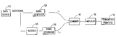
Fig. I is a top-level block diagram of an example transmitter system that
illustrates the
concepts of the invention.
Fig. 2 is a block diagram illustrating an optical implementation of the
transmitter
system shown in Fig. 1.
Fig. 3 is a signal timing diagram showing segments of the first and second
complementary data signals generated by a transmitter system according to an
implementation
of the invention.
2
CA 02741903 2011-06-01
Fig. 4 is a diagram conceptually illustrating combining of the complementary
data
signals in an interleaved, non-overlapping manner.
Fig. 5 is a functional flow diagram illustrating the operations performed in
generating
the complementary data signals.
Fig. 6 is a block diagram illustrating an implementation of a receiver system
for
recovering data from the combined complementary data signals.
Fig. 7 is a functional flow diagram illustrating the operations performed in
receiving
and detecting the complementary data signals to recover data.
DETAILED DESCRIPTION
Described herein is a technique for increasing the signal gain of a
transmitted signal in
a communication system. A first data stream is generated by modulating a first
signal using
on-off keying (OOK). A complementary second data stream is generated by OOK
modulating
a second signal with an inverted version of the first modulation, such that
the second signal is
"off' when the first signal is "on" and vice versa. The first and second
signals have respective
first and second different optical wavelengths. The complementary first and
second signals
can be combined such that the power of the first signal is interleaved with
and temporally non-
overlapping with the power of the second signal. The combined signal is
substantially a
constant power signal in which the first wavelength signal is "on" when the
second
wavelength signal is "off." In effect, the resulting signal is a frequency
shift keying (FSK)
modulated signal generated by combining two complementary OOK modulated
signals.
At optical wavelengths, the combined first and second signals can be amplified
with
the same optical amplifier, such as an erbium-doped fiber amplifier. The
optical amplifier
sees what appears to be a continuous wave (CW) constant power signal. Since
the full power
of the amplifier is used continuously during transmission, the FSK signal
enjoys a 3 dB gain
relative to the individual constituent OOK modulated signals. Instead of
having no signal to
amplify during "off' periods of the original (first) OOK signal, the optical
amplifier is used to
amplify the second wavelength signal during the "off' periods of the first
wavelength signal.
Thus, instead of an x watt optical amplifier producing a signal with an x/2
average power, the
x watt optical amplifier produces a signal with an average power of x, and the
full peak power
3
CA 02741903 2011-06-01
of the amplifier is obtained in the transmitted data signal. Nevertheless,
this power gain is
achieved without significantly increasing the size, weight, and hardware
complexity of the
transmitter system relative to a system that uses OOK modulation and without
increasing the
wall plug power cost of the system.
Fig. I is a top-level block diagram of an example transmitter system that
illustrates the
concepts of the invention. A data signal is supplied by a data source 110,
such as a modem.
The data signal can be an electrical signal encoded with data to be
transmitted to a far-end
terminal. For example, data source 110 can encode data into the data signal
via on-off keying
(OOK) at a selected modulation rate suitable for optical transmission. With
OOK modulation,
the data signal sequentially alternates between a first power level and a
second power level
that is preferably a very low or zero power level, resulting in intervals of
full power and
intervals of substantially no power. A logical "0" can be represented by the
absence of power
over an interval, and a logical "1" can be represented by the presence of
power over an
interval, or vice versa. Optionally, an encoding scheme can be employed which
ensures an
on/off duty cycle of about 50% (i.e., the signal is at full power about half
of the time and at
zero power about half of the time). To convey information rapidly, the
modulation rate can be
at least one megahertz (MHz) and may be many orders of magnitude higher,
possibly
exceeding one or many gigahertz (GHz).
The data signal can be used to transmit virtually any type of information or
data
including, but not limited to: sensor data, navigation signals, voice/audio
signals, image
signals, video signals, data relating to an application running on a
processor, control signals,
and overhead or communication protocol signals (e.g., relating to the
communication protocol,
handshaking, routing, equipment configuration, etc.). In particular, sensors
that collect
information for intelligence, surveillance, and reconnaissance generate a
substantial amount of
data and can benefit from the high data rates employed in optical
communications to transmit
the information in a reasonable amount of time.
The data signal is supplied to a first signal path and to a second signal path
that is in
parallel with the first signal path. A first signal generator 120 is disposed
on the first signal
path and converts the data signal to a first signal at a first wavelength X1,
which is supplied as
4
CA 02741903 2011-06-01
an output. The output first signal preserves the data modulation contained in
the original data
signal.
An inverter 125 and a second signal generator 130 are disposed on the second
signal
path. Inverter 125 generates an inverted version of the data signal. In
particular, the output of
inverter 125 is an OOK modulated signal in which the signal is "on" during
intervals in which
the original data signal is "off' and vice versa. Signal generator 130
converts the inverted data
signal to a second signal at a second wavelength a,2 that is different from
the first wavelength
Xi. The second signal preserves the data modulation of the original data
signal, but the second
signal has power during time intervals in which the first signal has
substantially no power, and
the second signal has substantially no power during the time intervals in
which the first signal
has power. While shown in Fig. I upstream of signal generator 130, inverter
125 can be
located downstream of signal generator 130.
A combiner 140 receives the first and second signals from first and second
signal
generators 120 and 130, respectively, and combines the first and second
signals into a
combined signal on a common output path. Due to inversion of the second signal
relative to
the first signal, within the combined signal, power attributable to the first
signal is interleaved
with and substantially non-overlapping temporally with power attributable to
the second
signal. The combined signal is supplied to an amplifier 150, which amplifies
the combined
signal. In this manner the same amplifier amplifies both the first and second
signals without
sacrificing full amplification of either signal. The amplified, combined
signal is then supplied
to a transmitter front-end 160, which transmits the combined signal via the
transmission
medium employed in the communication system. In the case of free-space
communications,
the front-end 160 can be an antenna (e.g., for RF signals) or optics (e.g.,
for optical signals).
In the case of transmission media such as wire, cable, or optical fiber, the
combined and
amplified signal can be supplied directly to the transmission medium without a
free-space
interface.
Fig. 2 is a block diagram illustrating an optical implementation of the
transmitter
system shown in Fig. 1. In this example, the first signal generator 120
comprises an optical
signal generator such as a laser module 210. By way of a non-limiting example,
laser module
210 can be a tunable laser seed module such as a commercially available small
form-factor
CA 02741903 2011-06-01
pluggable (SFP) laser module that provides an interface between a device
supplying data (e.g.,
Ethernet traffic) and an optical fiber. In this example, laser module 210
converts the data
signal supplied from data source 110 in electrical form to an optical signal
at the first
wavelength 2 and conveys the first signal on an optical fiber.
The inverter 125 on the second signal path comprises an electrical inverter
220, and
the second signal generator 130 on the second signal path comprises an optical
signal
generator such as a laser module 230, which can be similar to laser module
210. Inverter 220
receives the data signal in electrical form and generates an electrical output
signal that is the
logical opposite of the data signal (i.e., the output signal is a logical "1"
when the data signal
is a logical "0," and the output signal is a logical "0" when the data signal
is a logical "I").
The inverted data signal is then supplied along the second signal path to
laser module 230,
which converts the input electrical signal to an optical signal at the second
optical wavelength
X2 to produce the second signal, which is conveyed on an optical fiber.
By way of example, the optical wavelengths of the first and second signals can
be in
the eye-safe region of the spectrum (i.e., wavelengths longer than about 1.4
microns), such as
wavelengths in the telecommunications C and L bands or between about 1530 nm
and 1600
nm. These wavelengths permit commercially-available optical components to be
used in the
laser transceiver. Nevertheless, the invention is not limited to any
particular range of optical
wavelengths. Thus, as used herein and in the claims, the term "optical" refers
generally to the
range of wavelengths of electromagnetic signals within which "optical"
equipment (e.g.,
optical communication equipment, transmitters, receivers, etc.) typically
operates, including
the visible spectrum, infrared wavelengths, and ultraviolet wavelengths.
Fig. 3 is a timing diagram showing representative portions of the first and
second
signals one above the other for comparison. The first signal comprises a
sequence of logical
ones and zeros resulting in a signal that alternates between a first state in
which power is
present and a second state in which substantially no power is present in
accordance with the
data values being transmitted. The second signal contains the same data
modulation as the
first signal, except that the second signal comprises inverted data whose
logical state is the
opposite of that of the first signal, such that the second signal contains
power during the
intervals in which the first signal does not contain power, and the second
signal does not
6
CA 02741903 2011-06-01
contain power during the intervals in which the first signal contains power
(i.e., the first and
second signals are complementary).
Referring again to Fig. 2, an optical combiner such as a fiber combiner 240
combines
the first and second signals in fiber. Fig. 4 illustrates the effect of
combining the first and
second signals. In the combined signal, the portions of the first signal
containing signal power
(shown with left-to-right upward-slanting cross hatching in Fig. 4) are
interleaved with the
portions of the second signal containing signal power (shown with left-to-
right downward-
slanting crosshatching in Fig. 4) such that the power of the two signals is
substantially non-
overlapping temporally. The two signals are still distinguishable by virtue of
their different
wavelengths. Note that both signals within the combined signal essentially
contain the same
data and are, in effect, redundant. In other words, in principle, the same
encoded data could
be recovered from either signal without the complementary signal (although it
may be
necessary to account for inversion of the data modulation in the case of the
second signal).
The resulting combined signal is essentially a frequency shift keying (FSK)
modulated signal
constructed from two complementary OOK modulated signals, wherein logical ones
are
represented with one frequency and logical zeros are represented with a
different frequency.
In the case of free-space transmission, another benefit to this scheme
compared to a
standard OOK modulated signal is the covertness of the modulated signal. If a
third party
observes the signal with a detector, only a CW (continuous wave), constant
power signal will
be seen. Unlike an OOK signal, the underlying modulation will not be visible
unless the
detector is sophisticated enough to filter the signal spectrally. Thus, the
combined signal also
provides a Low Probability of Intercept (LPI) relative to a standard OOK
signal.
As shown in Fig. 2, the amplifier can be implemented with a single mode erbium-
doped fiber amplifier (EDFA) 250 whose output can be supplied to a collimator
260 which
receives the combined signal at the fiber end and supplies a free space
collimated beam to
transmitter optics. According to another option, the output of EDFA can be
supplied to a fiber
optic transmission medium. The wavelengths of the first and second signals
(x,, k2) can be
selected to be within the amplification band of EDFA 250. If, for example,
EDFA 250 has a
peak power of 5 watts, a typical data stream, with an equal number of logical
zeros and ones,
will have an average data power of 2.5 watts. By using the logical zero slots
of the first signal
7
CA 02741903 2011-06-01
for transmission of the second signal, the combined signal will have an
average power of 5
watts (i.e., substantially equal to the peak power).
While the system shown in Fig. 2 involves optical signals being conveyed,
combined,
and amplified via optical fibers and a fiber amplifier, the principles of the
invention can be
employed in the context of any of a wide variety of signal conveying,
combining, and
amplifying mechanisms. For example, the complementary signals can be combined
and
amplified in free space rather than in fiber. More generally, the principles
of the invention can
be employed in systems using non-optical wavelengths, such as RF systems.
Fig. 5 is a functional flow chart summarizing the operations performed to
generate
complementary first and second optical signals, as described above in
connection with Figs. 1-
4. In operation 510, a first signal modulated with data is generated at a
first optical
wavelength. In operation 520, a complementary second signal that is an
inverted version of
the first signal is generated at a second optical wavelength. The first and
second signals are
optically combined in operation 530 to produce a combined signal in which
power attributable
to the first signal is interleaved with and substantially non-overlapping
temporally with power
attributable to the second signal. The combined signal is then amplified
(operation 540) and
transmitted (operation 550).
At the receiving end, the combined signal can be separated into the
constituent first
and second signals, and a differential detection scheme can be employed to
recover the data
signal. A block diagram of an example of a receiver system for detecting the
interleaved first
and second signals is shown in Fig. 6. The combined signal is received via a
receiver front
end which, in the case of an optical system, can be receiver optics 610 (e.g.,
lenses, mirrors,
etc.) that direct the signal along a signal path for processing. According to
other
implementations, the signal may arrive at the receiver via an optical fiber, a
wire, a coaxial
cable, etc. In the example shown in Fig. 6, the combined signal can be
directed from free
space into an optical fiber or remain a free-space beam. A beamsplitter 620
separates the
combined signal into the first signal at the first wavelength 2 and the second
signal at the
second wavelength X2. For example, beamsplitter 620 can be configured to
reflect
substantially all light at the first wavelength ?1 and to transmit
substantially all light at the
8
CA 02741903 2011-06-01
second wavelength X2 or vice versa. The first and second signals are then
separately conveyed
along parallel paths.
After separation, the second signal is supplied to an optical detector 630
configured to
convert the optical second signal to an electrical signal. Optical detector
630 can be any
photo-electric detector (photodetector) capable of converting an optical
signal into an
electrical signal, such as a photodiode (e.g., a PIN diode or an avalanche
photodiode (APD)).
The output electrical signal preserves the modulation contained in the input
optical signal. In
the example shown in Fig. 6, the first optical signal reflected by
beamsplitter 620 is directed
by a mirror 640 along another path to another optical detector 650, which
converts the optical
first signal into an electrical signal in substantially the same manner that
optical detector 630
converts the second signal.
The first and second electrical signals are respectively supplied to the non-
inverting
(+) and inverting (-) inputs of a differential amplifier 660 (e.g., an
operational amplifier)
configured as a comparator whose output depends on the difference between the
amplitudes of
the first and second signals. For example, if there is more power on one input
than the other,
the output signal is in one logical state, and if there is more power on the
other input, the
output signal is in the other logical state. In effect, the differential
detection results in a 3 dB
signal power gain at the output of the differential amplifier 660 relative to
detection of an
individual OOK signal. This 3 dB gain is due to the fact that an OOK signal
represents the
two logical states with full power and no power signals, respectively, such
that a detection
threshold must lie between these two states. The differential signal generated
from the dual
OOK signals produces a more discernable difference between the representations
of the two
logical states in the output signal.
The output of the amplifier 660 is a sequence of logical ones and zeros
representing
the original data and is supplied to data handling circuitry 670 to recover
the original data
transmitted via the combined signal. The differential detection also helps
remove background
light, since any interference would be added equally to both detectors and be
present at both
amplifier inputs, but would not affect the offset between the two signals. By
continuously
using the full power of the transmitter system and detecting the transmitted
signal in this
manner, a 3 dB power gain can be realized relative to a comparable system
employing OOK
9
CA 02741903 2011-06-01
modulation on a single signal. Nevertheless, the second signal is generated
and these power
gains are realized without substantially increasing the size, weight,
complexity, power
consumption, and cost of the optical transmitter system.
Fig. 7 is a functional flow chart summarizing the operations performed to
recover data
from a received optical signal that is the combination of first and second
complementary
signals, as described above in connection with Fig. 6. In operation 710, a
combined optical
signal containing first and second complementary signals is received. In
operation 720, the
combined signal is split into the first signal on a first path and a second
signal on a second
path. The first and second optical signals are converted to electrical signals
in operation 730
and respectively supplied to the two inputs of a comparator to produce a data
signal at the
output of the comparator in operation 740.
The complementary first and second signals can be generated by any of a wide
variety
of devices, and the invention is not limited to these examples. Regardless of
the particular
mechanisms used, creation of the signals requires that the signals can be
combined in an
interleaved manner without the power attributable to the two signals
substantially temporally
overlapping so that the signals can be fully amplified by a common amplifier.
This is
accomplished in this example by having the second signal include the same data
modulation
pattern as the first signal but in an inverted form.
The transmitter system for generating complementary first and second
interleaved
signals described herein can be employed in an optical (e.g., laser)
communication terminal
designed to operate in a laser communication system with moving platforms,
where the
relative positions of terminals change over time. The system can include, for
example,
terminals mounted on airborne platforms, satellites, ships, watercraft, or
ground vehicles, as
well as stationary terminals that communicate with terminals mounted on moving
platforms
(e.g., combinations of air-to-air and air-to-ground links).
While the invention has been described in the context of free space optical
communications, more generally the concepts of the invention can be used in
any optical
communication system including those that employ fiber optic transmission
media.
Moreover, while the signal generation techniques described herein are
particularly well-suited
CA 02741903 2011-06-01
for optical systems, the concepts of the invention are equally applicable at
other wavelengths,
including RF wavelengths.
Having described preferred embodiments of a new and improved technique for
increasing signal gain, it is believed that other modifications, variations
and changes will be
suggested to those skilled in the art in view of the teachings set forth
herein. It is therefore to
be understood that all such variations, modifications and changes are believed
to fall within
the scope of the present invention as defined by the appended claims. Although
specific terms
are employed herein, they are used in a generic and descriptive sense only and
not for
purposes of limitation.
11