Note : Les descriptions sont présentées dans la langue officielle dans laquelle elles ont été soumises.
CA 02742284 2016-04-28
License plates for a vehicle
Description
The invention relates to an identification device for a vehicle with a flat,
at least
partially electrically inductive identification device body, which has at
least one
indicia area and with at least one indicia, which is assigned to the indicia
area of
the identification device body, with the identification device body being
assigned
a data carrier which is contactlessly readable, and an antenna which is formed
by
the identification device body that is provided with at least one slit, and
the data
carrier is a data carrier which generates a magnetic field and the antenna.
The vehicle identification device according to the invention involves so-
called
license plates that are mounted on the front or rear of a vehicle body or on
its
front and rear bumpers, or adhesive identification labels that are stuck to a
glass
panel of the vehicle, in particular as supplementary identification.
Identification devices of the aforementioned types are frequently
counterfeited or
misused for a different vehicle. To prevent this, identification devices are
known
which feature a data carrier that can be read contactlessly. This data carrier
contains vehicle-relevant data about the vehicle to which the data carrier
belongs.
These data are read by means of an external reading device. A comparison of
the read data with the vehicle on which the identification device is used
allows
one to draw conclusions concerning misuse, in particular when the
identification
device has been assigned to a different vehicle.
Hitherto known identification devices with data carriers that can be read
contactlessly feature a separate antenna. The antenna is connected to the data
carrier with electric conductors for the transmission of the data. Such an
identification device is costly and susceptible to malfunction.
The object of the invention is to create a simplified identification device
with a
data carrier and an antenna.
An identification device, in particular a vehicle license plate, wherein the
data
carrier is inductively coupled to the slit, whereas the data carrier has a
chip and at
least one coil connected electroconductively thereto, and a carrier made of an
insulating or nonconductive material and the slit or the data carrier serves
simultaneously as an amplifier. This identification device has at least one
data
CA 02742284 2016-04-28
2
carrier, which generates a magnetic field, and an antenna, which is formed by
the
identification device body, which has at least one slit. The identification
device
body is made at least partially of an electrically conductive material, for
example
aluminum sheet. The result is an identification device with a transponder
comprising a data carrier, which generates a magnetic field, and an antenna.
The
slit in the at least partially conductive identification device body results
in an
inductive coupling of the data of the data carrier in the identification
device body
serving as an antenna. Here the antenna, in particular the slit or the data
carrier,
serves simultaneously as an amplifier. The data of the data carrier can thus
be
-I o read at a relatively large distance without any additional components
and also
without any connections of the data carrier.
According to a preferred development of the invention, it is provided that the
data
carrier is disposed within the slit in an electronically insulated manner, to
be
specific, preferably at a closed end of the slit. This makes it possible to
accommodate or integrate the data carrier in the identification plate body
without
requiring additional installation space and that the data carrier cannot be
seen
from the outside of the identification device.
Preferably, it is provided that the data carrier, in particular its
electrically
conductive components, make no contact, and in particular specifically no
electrically conductive contact, with the identification device body of the
identification device. To this end, a circumferential gap or intermediate
spacing is
formed between the conductive components of the data carrier and the slit in
the
identification device body, thereby resulting in a particularly effective,
contactless
coupling of the data carrier to the electrically conductive identification
device
carrier of the identification device. This coupling is made inductively by
means of
the magnetic field generated by the data carrier.
In a further preferred development of the identification device, the slit is
provided
with at least one opening, thus resulting in an enlargement in regions of the
slit.
Preferably, the opening is assigned to an end of the slit so that the slit end
is
enlarged by the opening. By arranging the data carrier in the region of the
enlargement created by the opening at one end of the slit, sufficient space is
also
created for larger data carriers in the identification device body. Here the
data
carrier is situated within the contour of the identification device carrier,
specifically
CA 02742284 2016-04-28
3
without coming into physical or electrical contact with it. The data carrier
cannot
be perceived in the interior of the identification device, thus providing an
invisible
electrical or electronic protection of the identification device.
It is preferably provided that the data carrier is fixed in the identification
device,
namely in the identification device body. Any type of non-conducting means can
be considered for fixing the data carrier in the identification device,
whereas
these means do not have to cover the entire surface of the identification
device.
In particular, fixation is carried out by means of at least one coating or
adhesive
layer which covers the identification device body at least partially. The
readability
of the data of the data carrier is not impaired by the electrically non-
conducting
coating or adhesive layer. Any attempt to tamper the data carrier would result
in
easily perceptible damage to the coating or adhesive layer. In an alternative
development of the invention, the data carrier is fixed in the slit or opening
by a
reflective film applied to the visible front side of the identification device
body. In
this case, the reflective film is demetallized at least in the region of the
data
carrier, the slit and/or the opening, and thereby made nonconductive.
A development of the identification device is conceivable in which the data
carrier
is disposed in a receiving depression in the identification device body. The
holding recess can be stamped into the identification device body. The data
carrier is then attached in this holding recess in an insulating manner to
prevent
its conductive components from making any conductive connections with the
identification device body made of conductive material. This thus results in a
magnetic or inductive coupling of in particular a slit of the data carrier to
the
identification device body. In the process, the identification device body
serves
not only as an antenna but preferably also as an amplifier at the same time,
thus
making it possible for the data of the data carrier to be read over a
relatively large
distance as well.
It is particularly advantageous to provide a base of the depression of the
holding
recess with a continuous opening that is smaller than the data carrier so that
the
data carrier can be fixed despite this opening and the depression. The opening
results in improved antenna function and, above all, in an improved
amplification
of the transmission power of the chip of the data carrier.
CA 02742284 2016-04-28
4
The data carrier preferably has at least one chip, preferably a passive Radio
Frequency Identification Chip (RFID chip), at least one electrically
conductive coil
and a carrier made of insulating material. The carrier facilitates the fixing
of the
data carrier in the identification device body. Above all, the carrier, being
a
nonconductor, ensures that the chip and the coil of the data carrier can be
integrated in the identification device and insulated with respect to the
identification device body, thus resulting in an inductive or magnetic
coupling of
the chip's signals to the identification device body of the identification
device.
A further identification device for achieving the object stated at the outset
is
io disclosed in the features of claim 13. In this case, the identification
device is a so-
called identification label which can be affixed on various parts of a
vehicle,
specifically on a bumper, on body parts or also on the windshield or other
glass
panes of the vehicle. The identification label has a main body comprising at
least
one layer, preferably a plurality of layers, and at least one data carrier
that can be
read contactlessly, for example a chip module. At least one of the layers is
at
least partially electrically conductive, while the remaining layers are
electrically
nonconductive. The electrically conductive layer is interrupted in the form of
a slit-
like gap, by means of which the electrically conductive layer becomes an
antenna. Here the antenna is formed by the electrically conductive layer with
the
at least one slit-like gap. By virtue of this arrangement, a separate antenna
is no
longer necessary for the transmission, in particular for the reading, of
signals of
the data carrier. The slit in the electrically conductive layer cannot be seen
on the
outer side of the identification label because the electrically conductive
layer can
have a relatively thin configuration, so that the slit hardly stands out
because the
conductive layer in the region of the slit must merely be nonconductive. The
antenna formed by the conductive layer with the slit-like gap has proven to be
quite effective for the wireless transmission of data, in particular as a
result of the
data carrier being configured as one that generates a magnetic field or which
can
be operated with a magnetic field. It has been shown that in this special
configuration of the identification label the antenna acts simultaneously as
an
amplifier.
A preferred embodiment of the invention provides that the data carrier is
accommodated and electrically insulated inside the slit-like gap in the
electrically
conductive layer. Consequently, the data carrier has no electrically
conductive
CA 02742284 2016-04-28
connection with the electrically conductive layer of the identification
device.
Instead, according to the invention there is an electromagnetic coupling of
the
data carrier to the electrically conductive layer of the identification device
such
that the electrically conductive layer with the slit-like opening can serve as
an
5 inductive antenna and preferably also as an amplifier for the data
carrier.
The data carrier is electrically insulated from the conductive layer of the
identification device preferably in that all conductive components of the data
carrier are spaced from the borders of the slit-like gap in the at least
partially
electrically conductive layer.
A further development of the identification device provides that the data
carrier is
fixed in the gap of the electrically conductive layer by means of at least one
additional, nonconductive layer of the main body. This results in a simple and
permanently reliable accommodation of the data carrier inside the electrically
conductive layer of the identification device.
It is conceivable to fix the data carrier in or on the slit-like gap in the
electrically
conductive layer by means of two nonconductive layers arranged on opposite
sides of the electrically conductive layer. As a result, the data carrier is
completely embedded in the main body. This arrangement makes it impossible to
tamper the data carrier as such efforts would necessarily result in damage to
at
least one layer, thus making any tampering easily ascertainable.
It is advantageous that the at least one layer employed for fixing the data
carrier
is a coating or a self-adhesive film. It is also conceivable that the at least
partially
electrically conductive layer is applied to one side of a film, for example by
vaporization. During vaporization, the slit-like gap in the electrically
conductive
layer can be formed at the same time. In this manner it is very simple to form
the
antenna by the partial attachment of the electrically conductive layer with
the slit-
like gap to a nonconductive backing film, with no electrically conductive
coating
being deposited in the region of the data carrier and/or of the gap.
Pursuant to an advantageous configuration of the invention it is conceivable
to
assign an authenticity feature to at least one of the layers of the
identification
device. This authenticity feature can preferably be executed as a hologram. It
is
very difficult to forge such a hologram. This therefore makes the
identification
CA 02742284 2016-04-28
6
device particularly tamper-proof. Preferably, the authenticity feature should
be
assigned to the electrically conductive layer.
The contactlessly readable data carrier also has a passive chip in the case of
the
film-like identification device, preferably a passive Radio Frequency
Identification
Chip (RFID chip), at least one coil and a carrier. Such a data carrier can be
manufactured in a relatively small format, thus making it easy to accommodate
the data carrier in the slit-like gap in the electrically conductive layer of
the
identification device.
Preferred embodiments of the invention will be discussed in more detail below
with reference to the drawings, which show:
Fig. 1 an identification device according to the invention with an
identification device carrier made of aluminum sheet and an
integrated data carrier,
Fig. 2 a cross-section through the identification device of Fig. 1,
Fig. 3 a top view of the data carrier,
Fig. 4 a second exemplary embodiment of an identification device in a
view according to Fig. 1,
Fig. 5 a third exemplary embodiment of an identification device in a
view
according to Fig. 1,
Fig. 6 a fourth exemplary embodiment of an identification device in a
view according to Fig. 2,
Fig. 7 a fifth exemplary embodiment of an identification device in a
view
according to Fig. 2,
Fig. 8 a cross-section through a flat identification device pursuant
to a
sixth exemplary embodiment of the invention,
Fig. 9 a film-like identification device pursuant to a seventh
exemplary
embodiment of the invention in a cross-section view analogous to
Fig. 8,
Fig. 10 top view of a film-like identification device pursuant to a
eighth
exemplary embodiment of the invention, and
Fig. 11 a cross-section through the film-like identification device of
Fig. 10.
CA 02742284 2016-04-28
7
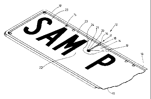
The identification devices 10 shown in Fig. 1 to 7 have a panel-shaped
identification device body 11 made of aluminum sheet. The identification
device
has a rectangular configuration, with its dimensions conforming to those of a
conventional motor vehicle license plate. The identification device body 11 is
5 provided with a folded edge 13 running around its border 12. This folded
edge 13
is pressed into the identification device body 11 by means of a forming
operation,
preferably by stamping.
Identification devices 10 of this type, commonly referred to as license plates
or
number plates, are usually attached to the front and back of a motor vehicle,
o specifically on the vehicle body and/or on the bumpers. For this purpose
the
identification device 10 has a number of mounting holes 15.
Within its front side 14 bounded by the folded edge 13 the identification
device 11
is provided with an indicia area 22. Located in the indicia area 22 is indicia
23 of
the identification device 10. Preferably, the indicia 23 is likewise applied
to the
indicia area 22 by stamping.
The indicia may consist of arbitrary characters, i.e. it is not limited to the
example
shown in Fig. 1, 4 and 5. In particular, any combination of letters, numbers
and
signs is possible in the composition of the indicia 23.
The identification device 10 is provided with a transponder. The transponder
has
an antenna 17 and a passive data carrier 20. The stored data of the data
carrier
20 are readable via the antenna 17 in a contactless manner. The data carrier
20
contains selected data about the vehicle to which the identification device 10
belongs. The data carrier 20 is equipped with a passive chip 74, which here is
configured as a passive Radio Frequency Identification Chip (RFID chip), a
coil
75, which is connected to the chip 74 in a electrically conductive manner, and
a
carrier 76 made of nonconductive material, for example plastic, which can be
configured as carrier film or a carrier body (Fig. 3). The passive RFID chip
comprising the data carrier 20 operates in a frequency range of 800 MHz to
1,000 MHZ. The RFID chip generates a magnetic field that is inductively
coupled
via the antenna 17.
The antenna 17 has a slit 18 within the electrically conductive identification
device body 11, namely in the aluminum sheet used to form the identification
CA 02742284 2016-04-28
8
device body 11. The antenna 17 is thus formed by the identification device
body
11 and the slit 18.
In the exemplary embodiment of Fig. 1, the slit 18 runs from a top edge 16 of
the
identification device body 11 approximately perpendicular to this top edge 16
into
the identification device body 11. The slit 18 is thereby open at one end.
However, the slit 18 can also proceed from any other edge of the
identification
device body 11. An opening 19 in the identification device body 11 is located
at
the end of the slit 18 opposite to the open end. This opening 19 enlarges the
closed end of the slit 18 lying in the identification device body 11. Here the
opening 19 corresponds to the shape or base area of the data carrier 20, thus
making it possible for the data carrier 20 to be inserted in the opening 19,
that is
to say it is encompassed by the periphery surface 21 of the opening 19, with
preferably a circumferential gap remaining between the opening 19 and the data
carrier 20. The data carrier 20 is electrically insulated from the
identification
device body 11 by its nonconductive carrier 76. This arrangement leads to an
inductive coupling of the data carrier 20 to the antenna 17.
In the identification device 10, the antenna 17, configured in the manner
described above, acts at the same time as an amplifier for the signal of the
chip
74, with the result that the relevant data of the chip 74 can be read at a
relatively
zo large distance from the identification device 10.
On its front side 14 provided with indicia 23, the identification device 10
has a
coating executed as a self-adhesive and preferably reflective film 24. The
film 24
covers the entire front side 14 of the identification device 10. The slit 18
with the
opening 19 and the data carrier 20 are thereby also completely covered by the
film 24. In the case of a reflective film 24 with metallic conducting
components, it
is provided that the reflective film 24 is supplied with a dennetallized
region 83 in
the regions where the data carrier 20, the opening 19 and the slit 18 are
located,
or that its layer structure is altered such that the reflective film 24 is not
conductive in the region of the data carrier 20, the opening 19 and the slit
18.
Consequently, the reflective film 24 is completely nonconductive in the entire
region of the slit 18 as well as that of the opening 19. Preferably, the
reflective
film 24 is also continuously nonconductive, in particular dennetallized, in
the
marginal areas bordering the slit 18 and the opening 19 with the data carrier
20.
CA 02742284 2016-04-28
9
Arranged at the rear side 26 of the identification device body 11 is a
nonconductive sticker 25. In the shown exemplary embodiment (Fig. 2) this
sticker 25 covers at least the region of the slit 18 with the opening 19 and
the
data carrier 20 located within. However, the sticker 25 can also cover a
larger
area, or can be configured as a self-adhesive film which covers the entire
rear
side 26 of the identification device 10.
The height of the data carrier 20, in particular of the carrier 76, is
approximately
the same as the thickness of identification device body 11. It is thereby
possible
to accommodate the data carrier 20 within the opening 19 and fix it there such
that it is located between and flush with the film 24 attached to the front
side 14
and the sticker 25 attached to the rear side 26 (Fig. 2).
The carrier 76 shown in Fig. 3 has a round base area, specifically, one shaped
like the opening 19. However, it is possible for the base areas of the carrier
76
and the corresponding opening 19 to assume different geometrical forms. The
surface of the opening 19 geometrically matches the base area of the data
carrier
20, namely that of its carrier 76. In the shown exemplary embodiment, the
opening 19 is larger than the carrier 76, whereby the carrier 76 is surrounded
by
a circumferential gap.
Fig. 4 shows an identification device 10 which differs from that of Fig. 1 and
2
only with respect to a modified slit 77. Both ends of this slit 77 are closed.
The slit
77 extends at a slight distance from and parallel to the lower longitudinal
border
of the identification device body 11, specifically in the region of the
indicia area
22. In the shown exemplary embodiment, the rectilinear slit 77 lies between
the
indicia 23 and the folded edge 13 at the lower longitudinal border of the
identification device 10.
One end of the slit 77 is assigned the opening 19, whose configuration
corresponds to the base area of the data carrier 20, namely of a carrier 76.
The
opening 20 is configured as in the exemplary embodiment of Fig. 1 and 2. The
data carrier 20 corresponds to the data carrier 20 shown in Fig. 3.
The only difference between the identification device 10 of Fig. 5 and the
identification device 10 of the previously described exemplary embodiments is
that the slit 78 runs a different course. This slit 78 is also closed at both
ends but
bends at a right angle, specifically preferably at its middle point.
Consequently,
CA 02742284 2016-04-28
half of the slit 78 extends in the region of a longitudinal edge, while the
other part
of the slit 78 runs parallel to the shorter transverse edge of the
identification
device 10. Again a closed end of the slit 78 is assigned an opening 19, whose
configuration corresponds to that of the data carrier 20. In the shown
exemplary
5 embodiment, the opening 19 with the data carrier 20 is located at that
end of the
angled slit 78 which is assigned to the longitudinal edge of the
identification
device body 11. However, the opening 19 with the data carrier 20 can also be
located at that end of the slit 78 which is assigned to the shorter transverse
edge
of the identification device body 11. The opening 19 corresponds to that of
the
o exemplary embodiment of Fig. 1. The data carrier 20 is also configured in
the
manner shown in Fig. 3. Reference is made here to the description of Fig. 1 to
3.
The identification device 10 of Fig. 6 differs from the previously described
identification devices in that the data carrier 20, which is basically of the
same
configuration as shown and described in Fig. 3, is arranged in a receiving
depression 79. Like the folded edge 13, the receiving depression 79 is stamped
into the identification device body 11 made of sheet metal, specifically being
stamped from the front side 14 of the identification device body 11, with the
receiving depression 79 thus being open on the front side 14 of the
identification
device 10. This allows the data carrier 20 to be inserted into the receiving
depression 79 from the front side 14. The depth of the receiving depression 79
is
selected so that the top side of the data carrier 20 pointing toward the front
side
14 of the identification device 10 fits approximately flush with the front
side 14 of
the identification device 10.
The receiving depression 79 is assigned to an end of the slit in the
identification
device body 11. This end of the slit does not need to have any opening 19
since
the opening 19 in this exemplary embodiment is replaced by the receiving
depression 79. The receiving depression 79 can be located at one end of the
slit
18, 77 or 78. The receiving depression 79 is stamped into the identification
device body 11 at the end of the respective slit 18, 77 or 78, with a base
wall 80
of the receiving depression 79 thereby having a continuous opening 81 formed
by
the end of the respective slit 18, 77 or 78. This opening 81, at least in its
width, is
smaller than the outer dimensions of the carrier 76 of the data carrier 20,
whereby the data carrier 20 does not fit through the continuous opening 81 in
the
base wall 80 of the receiving depression 79.
CA 02742284 2016-04-28
11
In the shown exemplary embodiment, the receiving depression 79 is stamped
into the identification device body 11 after its front side 14 has already
been
provided with the film 24. The film 24, which can be reflective film, thus
extends
across the base wall 80 of the receiving depression 79. In this case the data
carrier 20 is mounted by means of a nonconductive compound, such as an
adhesive 82, in the receiving depression 79, which is open at the top. In the
shown exemplary embodiment, the adhesive 82 also fills out an interspace
running around and encompassing the data carrier 20 between the outer walls of
the carrier 76 and the comparatively larger receiving depression 79 so that
the
receiving depression 79 is completely filled out by the data carrier 20 and
the
adhesive 82 (Fig. 6). In the exemplary embodiment shown here, the film 24 in
the
region of the receiving depression 79 and data carrier 20 does not have to be
demetallized. A label can be attached to the receiving depression 79 from the
front side 14 of the identification device 10.
Fig. 7 shows a further exemplary embodiment of the identification device 10
which, like the identification device of Fig. 6, has a receiving depression
79. The
receiving depression 79 has a configuration which is exactly the same as that
in
the identification device 10 of Fig. 6, which is why it is provided with the
same
reference numbers. In particular, here too the base wall 80 of the receiving
depression 79 has an opening 81, which is formed by one end of a slit 18, 77
or
78.
The exemplary embodiment of Fig. 7 deviates from the exemplary embodiment of
Fig. 6 in that in Fig. 7 the receiving depression 79 is stamped in the
identification
device body 11 before the film 24 is applied to the front side 14 of the
identification device body 11. Consequently, the inner side of the receiving
depression 79 is not coated with the film 24. Instead, the data carrier 20 is
inserted into the uncoated receiving depression 79. In this case, an
electrically
nonconductive insulation between the conductive sheet metal of the
identification
device body and the data carrier 20 is provided by the carrier 76, which is
made
of a nonconductive material. The data carrier 20 is also not firmly glued in
the
receiving depression 79. Instead, the data carrier 20 lies with its bottom
side on
the part of the base wall 80 which partially surrounds the opening 81, while
the
data carrier 20 is retained on its top side by the film 24, which in the case
of the
identification device 10 shown in Fig. 7 extends across the receiving
depression
CA 02742284 2016-04-28
12
79, specifically in a planar manner. In the shown exemplary embodiment, the
film
24 is a reflective film with conductive properties. For that reason the
reflective film
24 in the region of the data carrier 20 and receiving depression 79 is
electrically
nonconductive by virtue of a demetallized region 83. The data carrier 20
arranged
in the receiving depression 79 can therefore send amplified signals which can
be
received by a reader or similar apparatus at a relatively large distance from
the
identification device 10.
The slits 18, 77 and 78 have a width that is 1.5 to 2 times greater than the
thickness of the sheet metal used to form the identification device body 11.
o Depending on the sheet metal thickness, it is therefore possible for the
slit to
have a width ranging from 1.5 mm to 2.5 mm, preferably approximately 2 mm.
The length of the slit ranges from 100 mm to 200 mm, preferably approximately
160 mm. The diameter of the data carrier 20 lies in the range between 6 mm and
mm, preferably being approximately 8 mm. In the case of the identification
device 10, the thickness of the data carrier 20, in particular that of the
carrier 76,
can correspond approximately to the thickness of the sheet metal of the
identification device body 11.
A further identification device 30 is shown in Fig. 8. The identification
device 30
has the same format as the identification device 10 of Fig. 1 to 7
representing a
license plate. However, the identification device 30 is configured as a film-
like
identification label. Such identification labels are attached at the front
and/or rear
of a vehicle's body or on its front and/or rear bumper, specifically being
held in a
bracket or applied adhesively.
The identification device 30 has a passive data carrier 38 and possibly an
antenna as well, which serves as an amplifier. Here the antenna and the data
carrier 38 are designed in the same manner as the antenna 17 and the data
carrier 20 in the previous exemplary embodiment, and fulfill the same
respective
functions with the same features.
The identification device 30 has a main body 31 that is formed by a plurality
of
layers. A nonconductive carrier layer 32 in this case is employed to stabilize
the
shape of the identification device 30. This thin or film-like carrier layer 32
is made
of a thermoplastic synthetic material. One of its sides forms the rear side 40
of
.the identification device 30. An electrically conductive layer 33 is applied
to the
CA 02742284 2016-04-28
13
carrier layer 32, with a cover layer 39 being arranged over this electrically
conductive layer 33 in order to protect it. In the shown exemplary embodiment
the
cover layer 39 is configured as a self-adhesive film with a reflective
surface. At
the front side 41 of the identification device 30, which is visible from the
outside,
indicia 42 is applied, for example imprinted, on the cover layer 39.
The electrically conductive layer 33 has a slit-like gap. In the region of
this slit-like
gap the electrically conductive layer 33 is nonconductive. The slit-like gap
runs
from an edge of the electrically conductive layer 33, preferably from the edge
of
the identification device 30, approximately perpendicular to the edge, into
the
area of the identification device 30. The slit-like gap is thus open at an end
which
lies on the edge of the identification device 30. In contrast, an opposite end
of the
slit-like gap lying in the identification device 30 is closed. The slit-like
gap
provides the electrically conductive layer 33 with the properties of an
antenna, by
means of which the chip 74 of the data carrier 38 can be read in a contactless
manner.
The slit-like gap has at its inner, closed end an enlargement 37 in the
electrically
conductive layer 33. Arranged in the region of this enlargement 37 is the data
carrier 38. Here the enlargement 37 corresponds to the shape or base area of
the
carrier 38. Preferably, the enlargement 37 is somewhat larger than the data
carrier 38 so that the data carrier 38 is annularly spaced from the borders of
the
enlargement 37.
The electrically conductive layer 33 is formed by the vaporization of an
electrically
conductive material onto a nonconductive film. The nonconductive film is not
vaporized in the region of the slit-like gap and the enlargement 37 so that no
electrically conductive layer 33 is present in these regions and thereby
forming
the slit-like gap and the enlargement 37. As an alternative, the gaps and the
enlargements 37 can also be formed by a demetallization of the overall
electrically conductive layer 33.
The data carrier 38 is fixed within the enlargement 37 of the slit-like gap in
the
electrically conductive layer 33 by the cover layer 39 on the side of the
electrically
conductive layer 33 and by the carrier layer 32 on the other side of the
electrically
conductive layer 33. The data carrier 38 is approximately just as thick as the
electrically conductive layer 33 and can thereby be accommodated in the slit-
like
CA 02742284 2016-04-28
14
interruption in such a manner that it does not project beyond the front and
rear
side of the electrically conductive layer 33 and is therefore not perceivable
from
the outside of the identification device 30. To this end the carrier 76 of the
data
carrier 38 has a film-like configuration.
In a deviation from the illustration in Fig. 8, the slit-like gap can also be
closed at
both ends by being configured as a rectilinear strip or as an angled strip
having
the footprint of the slits 77 and 78 of Fig. 4 and 5, respectively. The
enlargement
37 is then arranged at one end of the slit-like gap.
The constructive design of a further exemplary embodiment of a identification
o device 50 is shown in Fig. 9. The identification device 50, like the one
in the
previous exemplary embodiment (Fig. 8), is configured as an film-like
identification label. The identification device 50 is also provided with a
data carrier
54 and an antenna 59. In this case the data carrier 54 and the antenna 59 are
designed in the same manner as the data carrier 38 and the antenna of the
exemplary embodiment of Fig. 8 and have the same characteristics.
The identification device 50 has a nonconductive carrier layer 51 auf. An
electrically conductive layer 52 is applied to this carrier layer 51. Arranged
on the
electrically conductive layer 52 is a nonconductive cover layer 55. This cover
layer 55 comprises a self-adhesive film or paint layer.
lndicia 57 is provided, for example imprinted, on the front side 56 of the
identification device 50, which is visible from the outside. An additional
nonconductive protective layer 58 is provided to protect the indicia 57 from
external mechanical influences. This protective layer 58 is transparent in
order
not to diminish the legibility of the indicia 57. In the shown exemplary
embodiment it is a self-adhesive film, but can also be a paint layer.
The electrically conductive layer 52 has a gap 53 which forms the antenna 59,
in
other words, it namely has the effect that that the electrically conductive
layer 52
serves as an antenna 59 and, if required, also as an amplifier. The gap 53 is,
as
in the previous exemplary embodiments, configured as a slit-like gap 53 that
is
open at one end and which has an enlargement at its closed end; however it can
also be closed at both ends.
CA 02742284 2016-04-28
The passive data carrier 52 is inserted within the slit-like gap 53 of the
electrically
conductive layer 52. The data carrier 54 is spaced from all borders of the gap
53
and is thereby separated and insulated electrically and mechanically from the
electrically conductive layer 52. In the case of the identification device 50,
the
5 carrier layer 51 and the cover layer 55 fix the data carrier 54 in the
gap 53 due to
the latter being arranged between the two layers.
A further exemplary embodiment of an identification device 60 according to the
invention is shown in Fig. 10 and 11. This identification device 60 can be
smaller
than the identification devices 10, 30, 50 of the previous exemplary
10 embodiments. Such identification devices 60 are preferably affixed to a
window
pane of a vehicle as a supplementary identification. For example, the
identification device 60 is adhesively affixed to the inner side of a
windshield 70
so that it can be seen from outside the vehicle.
The identification device 60 has a data carrier 66 and an antenna 71. The data
15 carrier, as in the case of the previously described exemplary
embodiments, is a
passive RFID chip 74 which operates in the frequency range of 800 MHz to
1.000 MHz and generates a magnetic field. The data carrier 66 also contains
data relating to the vehicle to which the identification device 60 belongs.
These
data can be read contactlessly via the antenna 71.
The identification device 60 is also configured as a film-like identification
device
60. It has a main body 61 which comprises a plurality of layers. lndicia 63 of
the
identification device 60 are applied to a nonconductive carrier layer 62. A
nonconductive adhesive layer 64 is provided on the side of the carrier layer
62
bearing the indicia 63. An electrically conductive layer 65 is located on the
carrier
layer 62. The electrically conductive layer 65 is connected to the carrier
layer 62
by means of the adhesive layer 64. In addition, the main body 61 has a
nonconductive cover layer 68 which is applied over the electrically conductive
layer 65.
In the shown exemplary embodiment the electrically conductive layer 65
comprises a metallic film or a nonconductive film vaporized with a metal
layer.
The electrically conductive layer 65 has a visible authenticity feature, for
example
a hologram, which is not represented in any further detail in the Figures. To
CA 02742284 2016-04-28
16
ensure the visibility of the hologram and the indicia 63, the adhesive layer
64 and
the carrier layer 62 are transparent.
The electrically conductive layer 65 has a slit-like gap 67. The slit-like gap
67
along with the electrically conductive layer 65 forms the antenna 71. The slit-
like
-- gap 67 is assigned to the data carrier 66, which is arranged in an
enlargement 72
of the slit-like gap 67 within the electrically conductive layer 65. The
electrically
conductive layer 65 has an electrically nonconductive configuration in the
regions
of the slit-like gap 67 and the enlargement 72, as well as in the adjacent
marginal
regions if necessary, in that here a conductive coating is omitted or the
-- electrically conductive layer 65 is demetallized. The data carrier 66 is
spaced
apart from all borders 73 of the enlargement 72 and is thereby at least
electrically
insulated from the electrically conductive layer 65. This thereby allows for a
completely contactless inductive coupling of the data carrier 66 to the
antenna 71
or to the electrically conductive layer 65 of the identification device 60.
-- The cover layer 68 fixes the data carrier 66 within the electrically
conductive layer
65, thus making it inaccessible to tampering. In addition, the opaque cover
layer
68 serves as an optical background for the hologram as well as for the indicia
63.
The identification device 60 is otherwise configured in such a manner that it
is
destroyed by any attempt to tamper with it or remove it from the windshield 70
of
-- a vehicle.
CA 02742284 2016-04-28
17
TNJ-66-WO
4 November 2009/5919
List of designations
idenlification device 53 gap
11 identification device body 54 data carrier
12 border 55 coyer Layer
13 folded edge 56 front side
14 front side 51 indicia
15 mounting hole 58 prOtbCtive layer
16 top edge 59 antenna
11 antenna 60 Identification device
18 Wit 61 main body
19 opening 62 carrier fayer
20 data carrier 63 radicle
21 periphery surface 64 adhestve layer
22 indicpa rarea 65 electrically conductive layer
23 indicra 66 data carrier
24 film 61 slit-like gap
25 sticker 68 cover layer
26 rear side 69 adhesive layer
30 identification device 10 windshield
31 main bOdy Ii ifltflfla
32 carrier Layer (2 enlargement
33 electrically conductive la)er 13 border
34 Wit-like gap (4 chip
35 edge is coil
36 an:enna 16 carrvet
ereargenlent II slut
30 data c.arber /8 slut
39 cover layer (9 receiving depression
40 rear side 80 base wall
41 front side 81 opening
42 odic:a 82 adhesive
50 identification device 83 demetallized reoion
51 carrier layer
52 electrically conductive layer