Note : Les descriptions sont présentées dans la langue officielle dans laquelle elles ont été soumises.
CA 02743955 2011-05-17
WO 2010/057263 PCT/AU2009/001514
-1-
RADIO FREQUENCY TRANSPONDER SYSTEM
FIELD
The present invention relates to a radio frequency transponder, a radio
frequency
transponder system, and a process performed by the system. In particular, the
transponder
is passive and the system may be used for identifying and tracking items where
the
transponders are in close proximity, such as when applied to books of
libraries.
BACKGROUND
Radio frequency identification (RFID) systems are based around the use of an
RFID tag
which is a radio frequency transponder attached to an object and used to store
a unique
identification code for the object. The code is read from the tag by an RFID
reader of the
system. Most RFID systems employed in libraries use an RFID tag that includes
an
antenna and a microcontroller semiconductor chip that stores the unique
identification code
for the tag. In Australia, only about 6% of public libraries currently use
RFID systems for
identifying the items they hold. It is considered that one of the reasons for
the relatively
low adoption of RFID systems within libraries is the cost of the tags. The
primary cost
associated with tags including microcontrollers is the microcontroller itself.
A "chipless" RFID tag uses a transponder that is passive in that it does not
include any
active processing circuitry, such as a microcontroller. The absence of a
microcontroller
significantly reduces the cost. To compete with optical barcodes a chipless
RFID system
should have a reasonable read range (e.g. _> 30cm) and use tags that are small
in size,
flexible and printable to reduce cost. Surface acoustic wave RFID tags have
been adopted,
but are rigid and bulky making them unsuitable for many applications,
particularly in
libraries where the items, or assets, with tags are stacked in arrangements
where the tags
are in close proximity.
A chipless RFID tag has been proposed which consists of a set of resonant
dipoles and
CA 02743955 2011-05-17
WO 2010/057263 PCT/AU2009/001514
-2-
when interrogated is able to provide a signal that represents an RF barcode.
The tag relies
solely on a series of printed dipoles terminated in variable capacitors that
create a series of
resonant peaks that can be detected by a reader when interrogated. Another
chipless tag
that has been proposed includes a series of fractal structures where each is
resonant at a
different frequency and similarly can produce a backscattered signal when
interrogated that
represents a unique code. Detection, however, is based on backscattered
amplitude which
can be unreliable for many applications, particularly in libraries.
Difficulties also arise in
printing the proposed tags, such as when the tag includes structures gap-
coupled to a
microstrip line of the tag.
Other limitations associated with chipless printable RFID tags that have been
proposed are
their limited information carrying capacity (only 8 bits for time domain
responses and 34
bits for frequency domain responses) and the efficiency and accuracy of the
RFID readers
used with the tags. The reader systems should be able to: (i) compensate for
the limited
capacity of information that can be extracted from a chipless RFID tag; (ii)
read multiple
chipless tags in close vicinity; and (iii) discriminate between the items the
tags are applied
to quickly and efficiently.
Accordingly, it is desired to address the above or at least provide a useful
alternative.
SUMMARY
According to one aspect, the present invention provides a radio frequency
transponder,
including:
a substrate; and
at least one planar antenna on said substrate, said antenna having a shape
determining a corresponding resonant frequency of said antenna;
wherein said antenna causes a phase difference between backscattered signals
generated in response to excitation of said antenna by orthogonally polarised
interrogation
signals at said resonant frequency, and said phase difference represents a
code of said
antenna.
CA 02743955 2011-05-17
WO 2010/057263 PCT/AU2009/001514
-3-
The present invention also provides a radio frequency transponder system,
including:
the transponder; and
a reader for generating the interrogation signals and reading the
backscattered
signals to extract said code.
The present invention also provides a radio frequency reader for interrogating
a radio
frequency transponder, including:
a frequency interface unit for transmitting polarised interrogation signals
and
receiving backscattered signals from the transponder in response; and
a signal processing unit for determining a code of the transponder from phase
difference of said backscattered signals.
The present invention also provides a radio frequency process, including:
transmitting polarised interrogation signals;
receiving backscattered signals from a transponder in response; and
determining a code of the transponder from phase difference of said
backscattered
signals.
DESCRIPTION OF THE DRAWINGS
Preferred embodiments of the present invention are hereinafter described, by
way of
example only, with reference to the accompanying drawings, wherein:
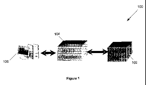
Figure 1 is a block diagram of an embodiment of a radio frequency transponder
system according to the present invention;
Figure 2 is a diagram of a stub loaded microstrip patch antenna for a tag;
Figure 3 is a graph of return signal loss against frequency for the antenna of
Figure
2;
Figure 4 is a graph of the relative phase of the backscattered signal against
stub
length of the antenna of Figure 2;
Figure 5 is a diagram of an embodiment of a radio frequency transponder
according
CA 02743955 2011-05-17
WO 2010/057263 PCT/AU2009/001514
-4-
to the present invention;
Figure 6 is a graph of the phase difference between backscattered signals in
two
orthogonal polarisations against absence or presence of stubs on antennas of
the
transponder of Figure 5, for different resonant frequencies;
Figure 7 is a diagram of a dual polarised stub loaded microstrip patch antenna
for a
tag;
Figure 8 is a graph of return and insertion losses against frequency for the.
antenna
of Figure 7;
Figure 9 is a radiation pattern for the antenna of Figure 7;
Figure 10 is a graph of the phase of the backscattered signal against
frequency and
for different stub lengths for the antenna of Figure 7;
Figure 11 is a diagram of a two-by-two array of patch antennas of Figure 7;
Figure 12 is a graph of radiation characteristics (boresight gain and side
lobes)
against element separation for the array of Figure 11 in a Corners layout;
Figure 13 is a radiation pattern for the array of Figure 11;
Figure 14 is a graph of radiation characteristics (boresight gain and side
lobes)
against element translation distance for positions of antennas in the array;
Figure 15 is a graph of radiation characteristics (boresight gain and side
lobes)
against element separation for the array of Figure 11 in a NSEW layout;
Figure 16 is a graph of the phase of the backscattered signal from the array
against
frequency and relative to stub length;
Figure 17 is a graph of backscattered phase difference against stub length for
the
antenna of Figure 7 and the array of Figure 11;
Figure 18 is a diagram of an embodiment of a chipless transponder with six two-
by-two patch antenna arrays, according to the present invention;
Figure 19 is a diagram of an embodiment of the radio transponder system;
Figure 20 is a block diagram of a reader of the radio transponder system;
Figure 21 is a diagram of an antenna of the reader;
Figure 22 is a block diagram of the reader reading a number of tags; and
Figure 23 is a graph of frequency against time illustrating frequency
modulated
continuous wave signal analysis for transmitted and received signals of the
reader.
CA 02743955 2011-05-17
WO 2010/057263 PCT/AU2009/001514
-5-
DETAILED DESCRIPTION
A radio frequency transponder system 100, as shown in Figure 1, is used for
radio
frequency identification (RFID) applications. The system 100 includes RFID
tags 102, at
least one RFID reader system 104 for interrogating or reading the tags using
radio
frequency interrogation or excitation signals, and an application system 106.
The
application system 106 is a computer system, such as produced by IBM
Corporation or
Apple Inc., having microprocessor circuitry, computer readable memory, and a
data
communications connection with the readers 104. The application system 106
stores and
runs application and database software to process data provided by a reader
104 and record
data associated with the items or assets on which the tags 102 are placed.
The RFID Tag
The tags 102 of the system 100 are each a passive and chipless (i.e. without a
microcontroller or microprocessor) radio frequency transponder that stores a
unique
identification code for each tag 102. The code is obtained from the phase data
of the back
scattered signal from the transponder in two orthogonal polarisation planes
when the
transponder is excited by radio frequency interrogation signals produced by
the reader
104.
The tag 102 includes an array of stub loaded microstrip patch antennas printed
on a
dielectric substrate using electrically conductive ink. The stub loaded
microstrip patch
antenna (SLMPA) of the tag 102 is based on a microstrip patch antenna 202,
shown in
Figure 2. The antenna 202 has a quadrilateral shape is printed on a substrate
204, has a
length L, width W and a stub 206 which is used to load the antenna. The stub
206 is
typically relatively thin with respect to the dimensions of said antenna.
According to Y.P.
Zhang, "Design and Experiment on Differentially-Driven Microstrip Antennas,"
IEEE
Trans. on AP, vol. 55 no. 10, 2007, pp 2701-8 ("Zhang"), the antenna 202 is
governed by
the following equations for a substrate with thickness h , resonant free space
wavelength
CA 02743955 2011-05-17
WO 2010/057263 PCT/AU2009/001514
-6-
2 and relative permittivity sr , which enables the length and width to be
selected based
on a selected values of sr (i.e. the choice of material), h and A,
L = All (1)
2 F~2+
W= -2AW (2)
2J (s.d+0.3)(L + 0.264) (3)
dW = 0.412t h (seg.-0.258)00.8)
-s'r+1+ r-1 (4)
2 2 1+12h
L
To obtain a maximum transfer of power from the antenna to the load, the
characteristic
impedance of the loading provided by the stub 206 needs to be matched to be
the same as
the real part of the input impedance of the antenna. This is desirable to
maximize the effect
that the load will have on the backscattered signal produced when the antenna
202 is
excited by the interrogation signal. This allows a conjugate matching
condition where the
load ZL = ZA*, where ZL is that antenna load impedance and ZA is the antenna
input
impedance. For simplicity, a 50 Ohm microstrip line is used for the stub 206
and according
to Zhang its offset from the centre of the edge of the antenna 202 is given
by:
Offset = W cos-' L 5(sr 1) - L (5)
/T 3sr+W 2
CA 02743955 2011-05-17
WO 2010/057263 PCT/AU2009/001514
-7-
For ease and cost of fabrication the antenna is loaded at its edge with a
distributed load
rather than a lumped load. The simplest sort of distributed load is an open
circuit
microstrip stub 206. The impedance of the open circuit microstrip stub 206 of
length SL
(Stub Length), with characteristic impedance Zo, can be calculated using
Richard's
Transformation (as discussed in D.M. Pozar, Microwave Engineering, Hoboken,
NJ: John
Wiley & Sons, 2005) and is given by:
ZIN = jZ0 cot (1i*SL) (6)
6 = (7)
g
where 2g is the guided transmission wavelength.
A SLMPA 202 was designed and simulated using 3D electromagnetic simulation
software
that provides a full-wave method-of-moments solver. The parameters of the
patch antenna
202 were L=39.2, W=47, Offset=7.4 and SL=O (all in mm). The substrate used was
Taconic TLX-0 (sr = 2.45) with a thickness of 0.7874mm and the conductor
thickness was
17 um. The simulated return loss is shown in Figure 3. The simulated results
of Figure 3
show a well matched antenna with a return loss peak of -24.9 dB at 2.4 GHz.
The width of
the patch 202 gives rise to multiple modes being excited and the fundamental
mode for the
orthogonal polarization is visible at 2 GHz.
The backscattering properties of the SMLPA 202 can be analysed using Radar
Cross
Section (RCS) analysis. The practical operating limits of using backscattered
signals from
an SLMPA can be analysed by examining the RCS characteristics of the antenna
202 when
illuminated with a plane wave linearly polarized in the E-plane. The main
phase
characteristics of the backscattered signal include a phase shift that depends
on the stub
length as shown in Figure 4. The phase shift data in Figure 4 is shown
relative to the
backscattered phase of an SLMPA 202 with no stub loading. The relative phase
or phase
difference follows a generally linear pattern according to the electrical
length of the
CA 02743955 2011-05-17
WO 2010/057263 PCT/AU2009/001514
-8-
loading stub. There is some discrepancy due to imperfections in the
fabrication however
they are not significant.
The tag 102 of the transponder system 100 includes a number of SLMPAs 500, as
shown
in Figure 5, which have different respective resonant frequencies to enable
the
backscattered signal from each antenna 500 of the tag to be isolated or
separated from each
other. The tag 102 is interrogated in two orthogonal planes using two
excitation
interrogation signals and the phase difference between the backscattered
signal in the two
planes is read and used to encode and determine the data of each antenna.
Using a phase
difference of two signals avoids fundamental issues associated with
environmental
conditions where the phase of the signal would change, and also avoids having
to
determine the spatial position of an antenna 500 or the tag 102.
Each SLMPA 500 is configured to resonate at the same frequency in both of the
two
orthogonal planes (El and E2) of the excitation signal. An SLMPA 500 can be
encoded
with a single bit of data by loading the antenna with no stub in one plane and
a stub of
length SL in the other plane. The unique bit of code associated with each
antenna 500 can
then be extracted by comparing the phase of the backscattered signal in the
two
polarisation states, which is then digitised by the reader 104 to represent a
1 or 0.
The tag 102 comprises of a plurality of SLMPAs 500, as shown in Figure 5,
printed using
electrically conductive ink on a paper or plastic substrate 502. The antennas
500 are
square so that the resonant frequency is the same for the orthogonally
polarised excitation
signals. Alternatively, the antennas 500 may be polygons of equal sides to
exhibit this
characteristic. The antennas 500 are of different lengths to correspond to
respective
different resonant frequencies. The antennas are each loaded by a respective
meandering
stub 504 having a stub length SL. The antennas 500 are printed adjacent each
other with
set spacing between them. Rather than simply loading the edge of each antenna
with the
stub, as shown in Figure 2, an insert feed is used for each stub 504. The
insert feed of each
antenna 500 is characterised by two parallel rectangular recess sections in
the antenna 500
to define an insert strip 506 having an insert length IL and an insert width
IW. The insert.
CA 02743955 2011-05-17
WO 2010/057263 PCT/AU2009/001514
-9-
506 is edge loaded by the meandering stub 504. The stub 504 is a microstrip
line that
meanders away from and back towards the antenna 500 to improve spatial
efficiency and
to increase the stub's characteristic impedance, allowing larger impedances to
be achieved
with shorter overall stub lengths.
To illustrate operation of the tag 102, a transponder with three square SLMPAs
500 with
side lengths (and widths) 38 mm, 41 mm and 44 mm and a spacing of 1 mm was
constructed so as to provide antennas with respective resonant frequencies of
2.52 GHz,
2.33 GHz and 2.17 GHz in both orthogonal planes. A meandering stub 504 of
length 10.9
mm and width 0.2 mm was added to represent and encode a 1 bit, whereas the
absence of
any loading stub on the antenna 500 was used to represent a 0 bit. The
transponder was
interrogated with linearly polarised interrogation signals having E field
vectors oriented in
the directions El and E2, as shown in Figure 5. The phase difference at
boresight in the
electric field was taken at 1 in, and the results obtained are shown in Figure
6 when
different combinations of absence and presence of the stub 504 were used. This
shows that
by merely processing the phase difference as the frequency is increased across
the resonant
frequencies, three unique binary bits can be extracted from a tag 102 using 3
square
SLMPAs 500. The phase difference read by the reader 104, however, varies
between 0 to
180 , and by using this entire phase difference a single antenna 500 of the
tag 102 can be
used to encode additional digital information. For example, a single antenna
500 can
produce code comprising a hexadecimal digit if phase differences with a
separation of
11.25 are detected. Encoding this phase difference with sufficient separation
is achieved
by changing the loading of the antenna by adjusting the length of the stub
504, for example
by 1 to 2 mm for the example transponder. Therefore at each resonant frequency
a
hexadecimal digit can be obtained from the tag 102.
An RFID tag 102 with n antennas 500 resonant at different frequencies fl, f2
... f,,-I, fn in an
array configuration, as shown in Figure 5 allows n hexadecimal digits to be
obtained by the
reader 104 when the tag 102 is interrogated by the orthogonally polarised
excitation signals
E1 and E2. The reader 104 scans across the frequencies fl to fõ to extract a
codeword (or
barcode) comprising the codes of each antenna 500. The codeword represents the
unique
CA 02743955 2011-05-17
WO 2010/057263 PCT/AU2009/001514
-10-
identification data (or ID) of the tag 102. The reader 104 converts the
magnitude of the
phase difference of the backscattered signals at each resonant frequency fl to
f71 into a
digital hexadecimal integer comprising a code and repeats the process at the
next resonant
frequency, until the stop bit of the codeword is found.
An alternative SLMPA 700 for use in the tag 102 is shown in Figure 7. This
SLMPA 700
is square and is loaded with two open circuit stubs 702 and 704 whose lengths
are
orthogonal to one another and extend from respective and adjacent sides of the
patch
antenna 700. This antenna 700 is dual-resonant and will exhibit a maximum
antenna mode
RCS at the desired resonant frequency by selecting the lengths and the
characteristic
impedance of the stubs, as discussed below. The antenna 700 has the advantage
that it
allows the signals in the H plane to also be utilised as a reference and
provide greater
discrimination. The SLMPA 700 is again fabricated of conductive material and
placed on
a dielectric substrate 706 which is placed on a conductive ground plane 708.
An SLMPA
700 was designed to resonate at 6.12 GHz on a 1.5 mm thick FR4 (sr = 4.9)
substrate, with
L = W = 10 mm, StubXL = StubYL = 1.5 mm and StubXW = StubYW = 0.2mm.
Operation of the circuit was simulated using the full-wave method-of-moments
solver and
the simulation ports were placed with an input impedance equal to that of free
space at the
end of the loading stubs, Portl at the end of StubY and Port 2 at the end of
StubX. The
return loss obtained for the SLMPA 700 is shown in Figure 8, where the S11 and
S22 plots
are the same and the S21 and S12 plots are the same and the subscripts
represent the input
and output ports examined. The two-dimensional radiation patterns for the
backscattered
signals in both the E and H planes are shown in Figure 9. This shows a good
return loss of
-22.2 dB at 6.12 GHz for both ports, and transmission leakage of power from
one port to
the other of -31.3 dB. The antenna has a gain of 4.4 dBi, and the radiation
pattern shows a
main lobe radiating in the outward normal direction of the patch (boresight).
If a single antenna is used to send and receive signals in each polarisation
state, the radar
range equation is given by
CA 02743955 2011-05-17
WO 2010/057263 PCT/AU2009/001514
-11-
PR G 2 A2 d"
(47r)3 r4 (8)
PT J
where,
PR = The received power (W)
PT= The transmitter power (W)
G = The reader antenna gain
r = The distance between the tag and the reader (m)
a = The Radar Cross Section (RCS) of the transponder (m)
Accordingly, the RCS can be varied with respect to frequency and create a
frequency
spectrum where distinct changes in the phase and amplitude are observable. The
RCS
consists of two components referred to as the antenna mode scattering and the
structural
mode scattering. The structural mode scattering is an unavoidable portion of
the RCS that
occurs due to the structure of the SLMPA itself, and exists for all possible
radar targets. In
general this scattering component does not exhibit a phase difference between
its
orthogonally polarized components. The antenna mode is a function of the
radiation
characteristics of the antenna itself and is designed using standard antenna
theory, as
described above.
The two scattering component parameters are defined with respect to the total
electric field
scattered from an antenna given by the following, as discussed in C. A.
Balanis, Antenna
Theory: Analysis and Design, 2nd edition, Hoboken, NJ: John Wiley & Sons, 2005
("Balanis").
Es(ZL)= ES(Z*)_ r*Et (9)
where,
Es (ZL) = The electric field scattered by the antenna when it is loaded with
an impedance
CA 02743955 2011-05-17
WO 2010/057263 PCT/AU2009/001514
-12-
of ZL
Es (ZA) = The electric field scattered by the antenna when it is conjugate
matched
ZA = The conjugate antenna input impedance
Im = The current induced when the antenna is in transmitting mode with a
conjugate
match
I, = The current induced when the antenna is in transmitting mode
r'* = The conjugate matched reflection co-efficient
E` = The time-varying electric field
The first term ES (Z*) in equation (9) represents the antenna mode scattering
and the
second term r*E` the structural mode scattering. Accordingly, changing the
loading
it
impedance of the antenna changes the antenna mode scattering component of the
RCS, as
discussed above for the SLMPAs 200 and 700.
With regard to the structural mode for the SLMPA 700, this can be determined
by
providing the antenna 700 with different loading stub lengths. In simulating
the RCS of
the antenna 700, the structural mode was found to be almost constant across
the frequency
band except for a clear resonant dip at 6.12 GHz. Outside of the resonant band
the
scattering consists of only the structural mode component, while in the band
it is a
combination of both the antenna and structural mode components. The resonance
appears
as a null in the RCS indicating destructive interference between the two
scattering
components. The phase response showed a smooth pattern except in the resonant
band
where a steady increase in the phase is observed as the loading stub is
extended. When the
length of the loading stub is varied from 1 to 2 mm while keeping all other
parameters
constant there is a clearly observable 82 degree phase shift at 6.12 GHz in
the
backscattered signal that only occurs within the SLMPA's resonant bandwidth,
as shown in
Figure 10. The resonant peak changes by 80 MHz for a 1 mm change in the
loading stub
length however this is not significant since the bandwidth of the resonance is
200 MHz and
the selected design frequency of 6.12 GHz remains in the operating band at all
times. An
CA 02743955 2011-05-17
WO 2010/057263 PCT/AU2009/001514
-13-
RCS E-field cross-polar plot showed that the axial ratio is never poorer than
15 dB, which
ensures the interrogation signal in one polarization does not substantially
influence the
backscattered signal in the orthogonal polarization. For multiple SLMPAs 700
to generate
multiple frequency signatures without substantial frequency overlap and thus
maximize the
amount of data that is stored on the tag 102, it is desirable that the phase
shift in the non-
resonant portions of the spectrum be substantially 0, as shown in Figure 10.
To increase the gain and introduce an element of symmetry in both the design
of the tag
102 and the backscattered signals produced, an array of SLMPAs is used. For a
two-by-
two array 1100, as shown in Figure 11, there are a number of factors that
affect the overall
radiation characteristics of the structure. These include the layout of the
array (linear,
planar etc.), the distance between the elements and the excitation amplitude
and phase of
each element. The transponder 102 is illuminated with a plane wave with
uniform
magnitude and phase and so the excitation amplitude and phase are equal.
The array 1100 consists of four identical SLMPAs 700 in a North, South, East,
West
(NSEW) layout as shown in Figure 11. The elements 700 are arranged
symmetrically
along a square of side length S. The inter-element spacing is described by the
parameter S
and the element orientation is described by the translation parameter D, which
has values
from -0.5*S to 0.5*S. The translation described by the parameter D for each
element is in
the clockwise direction indicated in Figure 11. The transponder ground plane
is square
shaped so that the structural mode scattering in each orthogonal polarization
is equal, and
its edge length is G.
For an array of identical radiating elements 700, the total radiated field as
a product of the
single element radiation pattern and the Array Factor (AF) is:
ETotal - ESingle element * AF (10)
For an N x M element planar array where the x separation is denoted by d,,
they separation
is denoted by dy and each element is excited by amplitude I1171 and phase (3,
the array factor
CA 02743955 2011-05-17
WO 2010/057263 PCT/AU2009/001514
-14-
is given by the following, as discussed in Balanis.
N M
AF = I I ej(m_1)(kdxsinGcosO+/3x) ej(n-1)(Mysin0sin0+/jy)
.i In ~j ml
n=I m=I (11)
For the 2x2 array layout of Figure 11 the array factor expands to
AF = e lk 2 sin sin ¾e jkD sin 0 cos 0 +e -Ik 2 sin B sin 0
e_ jkD sin 0 cos 0 +
jk 2 sin 0 cos jkD sin B sin ¾ -jk 2 sin 0 cos jkD sin sin 0
(12)
e e- +e e
There are two layouts or cases that exist which are referred to herein as the
NSEW case (as
shown in Figure 11) and the Corners case. The NSEW case exists when D = 0, and
the
Corners case exists when D =+0.5*S. In the Corners case Equation (12) becomes
ASsin0sin0 jkSsin0cos0 -jk-sin9sin0 -jk-sin 0cos0
AF = e 2 e 2 + e 2 e 2 +
jkSsinOcoso '-jk S sin 0 sin 0 -jkSsin0cos0 jkSsin0sin0 (13)
e 2 e 2 +e 2 e 2
Equation (13) is the same array factor as for a standard 2x2 planar array with
an inter-
element separation of S. The normalized form can be expressed as
AFõ sin(kSsin0sinq$) sin(kSsin0cosq5)
_ 1 - r 1
4 sink 2 sin 9 sin Ol sinl k S sin B cos O I (14)
According to Balanis the angle, 0, where the main and grating lobes of the
array factor will
exist is given by
6=sin-' mA =sin-' nA ,m,n=0,1,2...
Scoso Ssino (15)
CA 02743955 2011-05-17
WO 2010/057263 PCT/AU2009/001514
-15-
For the NSEW case equation (12) reduces to
jkSsin0sin0 -jkSsintsin0 jkSsinOcosq5 -jk -sin0cos0
AF=e 2 +e 2 +e 2 +e 2
(16)
This can then be normalized to
AF, = cosh k S sin 9(sin O+ coscb) I *Co sh k 4 sin 9(sin 0 - coscs)J
l J l (17)
Using the same procedure the maximum of the array factor will occur when
k 4 sin 0 (sin ¾ + cos 0) = mw, m = 0, 1, 2,... and
k S 4 sin 0(sin 0 - cos 0) = nom, n = 0, 1, 2,... (18)
which means that the main and grating lobes of the array will occur at
B=sin 2mA - sin 2nA m,n=0,1,2...
S(sin 0 + cos O)) ( S(sin 0 - cos 0)),
(19)
Equations (15) and (19) show that the larger the separation between the
elements defined
by the parameter S, the smaller the angle 0 where the 1st grating lobe will
occur. In other
words the closer the elements are to each other than the better the sidelobe
performance
will be. Also, the NSEW layout should have its optimum size with larger values
of S since
there is a factor of 2 in equation (19) that does not exist in equation (15).
The performance of the 2x2 SLMPA array 1100 was simulated using the full-wave
method-of-moments solver, and the radiation characteristics of the structure
relate directly
to the antenna mode scattering component. The array 1100 was illuminated by a
uniform
plane wave, and so the excitation for each port was uniform with no phase
offset, and to
CA 02743955 2011-05-17
WO 2010/057263 PCT/AU2009/001514
-16-
make the result comparable with that for a single SLMPA 700 only 25% of the
power used
previously was delivered to the whole array 1100.
The radiation patterns obtained are shown in Figures 12 and 13 for the Corners
case layout
with S = 0.61 2 (30 mm). The antenna array showed an improved maximum gain of
10.2
dBi with a side lobe of -13.9 dB, as shown in Figure 12. The side lobe level
becomes
larger as the element separation moves beyond half of the free space
wavelength, and then
multiple side lobes begin to appear. The antenna main beam gain is over 10 dBi
when
0.5 *X < S <),, as shown in Figure 12, while the side lobe level remains below
-3 dB.
To allow more flexibility in placement of the array elements the translation, -
0.5 * S < D <
0.5*S, was examined. As D increases in magnitude the array factor tends
towards the form
for the Corners case until the upper limit is reached. As D decreases in
magnitude the
array factor tends towards the NSEW case. Assuming that there is a uniform
change in the
radiation pattern for both, when D is varied the change in the boresight gain
and side lobe
level is as shown in Figure 14. Both curves are symmetrical around the point
where D = 0
as expected from equation (12) and this is where the minimum gain level is
observed. The
NSEW case exists when D = 0, and when S is varied to create the second design
curve for
placement shown in Figure 15, in this position it is better to have the
elements 700 farther
away than for the Corners case and the side lobe magnitude is smaller.
The above applies to the antenna mode scattering component, however the
structural mode
scattering is dependent on the overall size of the structure including the
substrate and the
ground plane. If the structure of the tag 102 is too large then the antenna
mode scattering
component will be too small compared with the structural mode scattering
component and
no longer observable. As the edge length G is increased the structural mode
scattering
increases significantly and the resonance is increasingly difficult to
observe. Also, when
the ground plane size is too small the radiation of the elements is disturbed
at the edges. To
determine the optimal size of the ground plane, the ratio of the total RCS and
the structural
mode component of the RCS at resonance for the array 1100 with SLMPAs of L =
10mm
was examined using RCS analysis, and the ratio was found to be largest when G
is 64 mm
CA 02743955 2011-05-17
WO 2010/057263 PCT/AU2009/001514
-17-
since this is the smallest size where the radiation of the antenna elements is
undisturbed.
With the size of the structure set the length of the loading stub was varied
to determine
corresponding changes in the scattering characteristics, as shown in Figures
16 and 17.
There was a slight change of 80 MHz in the resonant frequency within the
resonant
bandwidth of the optimally matched structure, and a co-polar phase plot
exhibited a shift of
189 for a change of 1 mm in the loading stub length (from lmm to 2mm). The
range of
the phase difference in the orthogonally polarized backscattered signals
realized by
changing the length of the loading stub by 1 mm is significantly greater for
the array: the
single element SLMPA 700 provided a phase change of 82 , whereas the array
1100
provided a phase change of 189 , as shown in Figure 17.
To illustrate operation of the tag 102 using the array structure 1100
discussed above a
prototype tag or transponder 1800 was designed. The transponder 1800, as shown
in
Figure 18, includes 24 SLMPA patch elements 700 and was designed to operate in
the
UWB spectrum from 3.1 to 10.9 GHz. The transponder 1800 contains six resonant
frequency signatures over the band from 4.5 to 6.75 GHz. As the tag 102 is
fabricated
using low cost conductive ink trace with a paper or plastic substrate, the
prototype
transponder 1800 operates on an inexpensive low performance PCB (FR4, Cr =
4.9)
substrate material with a thickness of 1.5 mm and a loss tangent of 0.025.
The six-signature chipless RFID transponder 1800 includes optimally matched
SLMPAs
700 at six resonant frequencies that do not interfere, and their parameters
are listed in
Table 1 below. Given the optimal spacing distance (S) for the Corners layout
is larger than
for the NSEW layout, the SLMPA arrays with shorter resonant wavelengths are
placed at a
smaller S, and with D closer to 0.
The transponder 1800 is symmetric for all resonant frequencies. Also, the non-
radiating
elements are placed or positioned so their mutual coupling effects are
symmetric as well,
and cancel each other out. This produces a main radiated beam for each
resonant
frequency that is aligned directly to boresight, with almost equal beamwidths
for all
CA 02743955 2011-05-17
WO 2010/057263 PCT/AU2009/001514
-18-
resonant frequencies. This is significant as it enables each antenna array and
thus the
transponder 1800 to be read from a fixed location.
Patch Width Resonant Frequency Stub Length Stub Width
mm (GHz) (mm) mm
9 7.24 1.1 0.2
6.47 1.5 0.2
11 5.91 1.6 0.2
12 5.45 1.75 0.2
13 5.06 2 0.2
10 14 4.7 2.3 0.2
Table 1
In Figure 18 the six sets of 2x2 SLMPA arrays are labelled with a number that
indicates
their patch width (9,10,11,12,13,14 mm). The highest frequency (smallest size)
SLMPAs
are placed on the inner layer which has space for two sets of 2x2 SLMPA arrays
(9, 10
mm). The outer layer includes the remaining four sets of 2x2 SLMPA arrays with
the
highest frequency array of these (11 mm) placed in the NSEW orientation, and
the lowest
frequency array (14 mm) in the Corners orientation. The intermediate frequency
arrays
(12, 13 mm) are placed in between NSEW and Corners layouts with IDS closer to
0 for the
higher frequency array. A 90 bend is introduced on the loading stubs, as
shown in Figure
18, to allow the elements to be placed closer together while minimizing mutual
coupling
effects.
The effects of altering the sub lengths for each two-by-two array in the
transponder 1800,
and the ability to create a difference in the backscattered phase shift for a
different stub
length were simulated using the full-wave method-of-moments solver, and the
obtained
values are summarised below in Table 2.
CA 02743955 2011-05-17
WO 2010/057263 PCT/AU2009/001514
-19-
Resonant StubYL StubYL
Patch Width Frequency Min Max Phase Shift
(mm) (GHz) (mm) mm (Degrees)
9 6.72 0.1 1.1 12.02
6.06 0.5 1.5 33.77
5 11 5.6 0.7 1.7 10.21
12 5.16 0.7 1.7 23.73
13 4.8 1 2 12.8
14 4.48 1.3 2.3 24.12
Table 2
To verify the simulated values, the transponder was also used in an
experimental
10 environment based on the operating principles described above, and a
summary of the
experimental results is shown below in Table 3.
Patch Width Resonant StubYL Max StubYL Min Phase Shift
(mm) Frequency (mm) (mm) (Degrees)
9 6.987 0.6 0 15.75
10 6.591 1 0 162.73
11 6.118 1.2 0 14.21
12 5.621 1.2 0 11.29
13 5.244 1.5 0 24.65
14 4.878 1.8 0 19.66
Table 3
The above shows an average measured phase shift of 41 at each signature
frequency for
the transponder 1800, and confirms the backscattered phase difference for each
frequency
signature can be controlled by adjusting the lengths of loading stubs of the
antenna
elements of the arrays. By increasing the operating frequency to higher
frequencies, such
as 40 GHz, the transponder size can be considerably reduced, such as to the
size of a credit
card or smaller. A tag 102 of this size can be fabricated on a plastic or
paper substrate by
printing the patch with conductive ink using a flexography printing process.
The stubs of
the patches, however, need to be varied for each tag 102 and to reduce cost
are printed
using conductive ink and an inkjet printing process. The ground plane can be
printed, like
the patch, using conductive ink and a flexography process.
CA 02743955 2011-05-17
WO 2010/057263 PCT/AU2009/001514
-20-
The Reader
The transponder system 100 utilizes two orthogonal polarization states during
both
transmission and reception when interrogating the tag. The separate
polarizations can be
provided at the reader 104 with a single dual-polarized antenna, or two
separate
orthogonally polarized antennas (API and AP2 for polarization states P1 and P2
respectively) as shown in Figure 19. The system can also function using a mono-
static
setup where the same antennas are used for transmission and reception or in a
bi-static
setup, as shown in Figure 19 where separate antennas are used for transmission
(API,T and
AP2,T) and reception (Apl,R and AP2,R). The reader 104 generates the
interrogation signal,
(1p, (f) and IP2(f)), at a frequency, f (GHz), and then divides the power
equally between
API,T and AP2,T. There are now two signals that propagate through free space
towards the
tag 102. The signals reach the transponder and are scattered according to its
Radar Cross
Section (RCS) characteristics. The tag 102 is designed so that the RCS
characteristics
differ in the orthogonal polarization states P l and P2, as discussed above.
The phase shift
is set so that the return signals (RPI(f) and RP20) that propagate back
towards the reader
have a phase difference of, A9N.
The signals are orthogonally polarized and travel through the same propagation
path, so
the path loss should be almost the same. The difference between the return
signals is only
due to differences in the scattering properties of the transponder for the two
orthogonal
polarization states. The phase difference is then converted into a set of
discrete bins (each
defining an accepted range of phase difference values) called phase signatures
that are
used to obtain digital data from the return signals at each resonant
frequency. For
example, for 7 frequency signatures, each frequency signature will contain a
discrete phase
difference between 0 - 180 , and each phase signature is resolved to the
nearest 10
creating 18 possible combinations for each frequency signature instead of the
standard 2
combinations (binary).
At a number of distinct resonant frequencies f to f N, a phase difference, cpN
can be
generated as defined in Equation (20).
CA 02743955 2011-05-17
WO 2010/057263 PCT/AU2009/001514
-21-
9N -- LRPI (fN) LRP2 \fN), where 0 <- I,N 1<-180 (20)
For a transponder system 100 configured to resolve the phase of the
backscattered signal
with a tolerance of t T/2 degrees then ( 180 / T) unique combinations or bins
can be used
for defining digital data. This means we can calculate the total number of
digital bits
("BITS") of information in the transponder which is presented in Equation
(21).
BITS = LN log2 (.9c-)J (21)
That is, the number of represented bits (BITS) is at least equal to the
highest integer value
equal to or less than (i.e. the "floor" of) a product of. the number of
frequency signatures;
and the base-2 logarithm of the number of bins. The number of bins is
determined by the
total detachable phase angle (180 ) divided by the resolution of the bins (T
).
For example, if 7 frequency signatures exit between 2 and 2.7 GHz, (meaning
that N = 7),
and each of the frequency signatures can be broken up into phase signatures
with a
tolerance, T/2 = 5 degrees, (so T = 10 degrees), the number of bits is:
BITS = [7log2(j0)j= 29
So in a 700 MHz section of the EM spectrum which previously held 7 bits of
data, 29 bits
can now be held.
The reader 104, as shown in Figure 20, operates at microwave frequencies, and
includes a
planar array transmit and receive antenna 2002, a high frequency interface
unit 2004
connected to the antenna 2002, and a digital control unit 2006 connected
between the
application system 106 and the high frequency interface unit 2004.
The digital control unit 2006 includes microcontroller circuitry to perform
digital signal
CA 02743955 2011-05-17
WO 2010/057263 PCT/AU2009/001514
-22-
processing on the data obtained from the RFID transponder 102 and to also
control
transmission of interrogation signals generated by the high frequency
interface unit 2004.
The control unit 2006 enables the reader 104 to communicate with the
transponders 102
wirelessly by performing modulation and anti-collision procedures and decoding
the
received data from the transponders 102. The unit 2006 includes a
microprocessor 2008, a
memory block 2010, analog-to-digital converters 2012 and a communications
interface
2014 for connecting to the application system 106.
The HF interface unit 2004 transmits and receives radio frequency ( RF)
signals, and
includes two separate signal paths to correspond with the two directional data
flows from
and to the transponder 102. A local oscillator 2050 (LO) generates the RF
carrier signal,
which is amplified by a power amplifier 2054, and the amplified signal is
transmitted
through the antenna 2002. A directional coupler 2056 separates the reader's
transmitted
signals and the received weak backscattered signals from the tag 102. The
directional
coupler consists of two continuously coupled homogenous transmission lines,
and if all
ports are matched, the power of the incoming and outgoing signals is divided
in the
coupler. The received backscattered signal is weak and a low noise amplifier
2058
increases the signal's amplitude before it is fed to an RF mixer 2052 with the
signal
generated by the local oscillator 2050 to produce an intermediate frequency
signal. The
intermediate frequency signal is processed by a gain and phase detector 2060
to generate
received data for the digital control unit 2006. The HF interface unit 2004 is
protected
from EM interference using metal cages.
The antenna 2002 includes two phased array antennas 2100 which each comprise,
as
shown in Figure 21: (i) a 3x2 element phased array antenna panel; and (ii)
associated
beamforming modules, as discussed in N.C. Karmakar, "Smart Antennas for
Automatic
Radio Frequency Identification Readers," Chapter 21, in Handbook on
Advancements in
Smart Antenna Technologies for Wireless Networks, Idea Group Inc., USA, pp 449-
473
("Karmakar V). Each beamforming module is a 4 bit digital phase shifter array
to control
the beam in a three dimensional (3D) plane. The phase shifter arrays, connect
to individual
element of the array antenna, control the values of p,, and Py in Equation
(11) which are the
CA 02743955 2011-05-17
WO 2010/057263 PCT/AU2009/001514
-23-
individual x- and y-plane phase shifts of elements, thus enabling beamforming
in a 3D
plane. To achieve generation of the orthogonally polarised interrogation
signals, two sets
of the beamforming modules or networks including the two array antennas 2100
are
operated coherently. The same beamforming networks that are used for
transmission are
also used for reception. The antennas 2100 are oriented in orthogonal planes
for the
polarisation diversity as described with reference to Figure 19. The
transmission and
reception paths are separated using a circulator or coupler as part of the
directional coupler
2056 of Figure 20. Dual-polarised sub-arrays can be used instead of the array
elements of
the antenna 2100 for high resolution dual-polarised signal transmission and
reception. A
number of antennas are used in various positions to exploit diversity. For
example, in an
active three-antenna configuration, a single pole three throw (SP3T) switch
activates three
adjacent array modules to collimate the in-phase beams in even further fine
resolution.
The antenna 2002 can then produce high gain scan coverage in 360 azimuth and
elevation
plane patterns. The antenna 2002 detects individual RFID tags 102, as shown in
Figure 22.
The exact bearing of each tag 102 from the reader 104 is calculated from the
beam position
of the antenna. For further fine tuning of the directional arrival (DoA) of
the tags' signals,
a post-processing Multiple Signal Classification (MUSIC) algorithm, as
discussed in C.
Sun and N.C. Karmakar, "Direction of Arrival Estimation with a Novel Single
Port Smart
Antenna," EURASIP Journal on Applied Signal Processing, 2400:9, 1364-1375.2004
("Karmakar 2") is used. Being very directive, the antenna 2002 filters out
side
interference. An alternative is to select frequencies with a reconfigurable
antenna.
The interrogating signals from the reader transmit antenna Tx, as shown in
Figure 22, are
sent to the tag 102 which returns frequency modulated echoes towards the
reader 104 and
the receive antenna Rx of the reader 104 receives the modulated echoes.
The reader 104 can use frequency modulated continuous wave (FMCW) signals from
the
transmit antenna Tx, with an instantaneous frequency that varies linearly in
time, as shown
in Figure 23. The receive antenna Rx receives modulated echoes after a time
delay, where
the echoes for tags with different resonant frequencies are received at
different times, as
shown in Figure 23. If the frequency response of the tags are well separated
in frequency,
CA 02743955 2011-05-17
WO 2010/057263 PCT/AU2009/001514
-24-
the FMCW echo signals will automatically be placed in different frequency bins
for
separate processing. In the signal processing both amplitude and phase of the
radar cross
section (RCS) are stored and processed. If the frequency response of the tags
are not well
separated, and tags' echoes overlap in the received time-frequency spectrum,
then the
added phases and amplitudes can indicate the number of tags which send the
echo signals.
For the phase encoded chipless RFID tags 102, the phase difference is
significant and the
phase vector addition of the echo signals is used to determine the presence of
the bits
encoded in each tag 102. The reader 104 is able to determine the number of
tags 102
which are collided in time and frequency spectrum. The received FMCW signals
are used
to distinguish moving tags 102 from stationary tags 102 by recording any
Doppler shift of
echo signals and the range of the tags 102. Time-domain windowing techniques
are used
to enhance the detection quality of echo signals. The reader 104 uses anti-
collision
measures, such as time of arrival (ToA), direction of arrival (DoA),
polarisation diversity
(PD), cross correlation of echo signals and frequency chirping of carrier
signals, to
discriminate between tags 102, particularly those in close proximity.
Many modifications will be apparent to those skilled in the art without
departing from the
scope of the present invention.
The reference in this specification to any prior publication (or information
derived from it),
or to any matter which is known, is not, and should not be taken as an
acknowledgment or
admission or any form of suggestion that that prior publication (or
information derived
from it) or known matter forms part of the common general knowledge in the
field of
endeavour to which this specification relates.