Note : Les descriptions sont présentées dans la langue officielle dans laquelle elles ont été soumises.
CA 02743985 2011-05-17
WO 2010/057307 - 1 - PCT/CA2009/001672
COMPRESSIBLE PHOTONIC CRYSTAL-BASED AUTHENTICATION
DEVICE
Technical Field
[0001] This disclosure relates to a compressible photonic crystal. In
particular, this
disclosure relates to a compressible photonic crystal-based authentication
device.
Backtround
[0002] Photonic crystals (PCs) are materials having a periodic modulation in
their
refractive index (Yablonovitch, Phys. Rev. Lett., 58:2059, 1987), giving rise
to a
photonic band gap or stop gap, in which electromagnetic waves within a certain
stop
band wavelength range are totally reflected. The wavelengths of the stop band
are
dependent on the distance between the periodic modulations in the crystal. The
reflected stop band wavelengths appear in the reflectance spectrum as a
distinct
reflectance peak known as a Bragg peak. The crystal may have a one-, two-, or
three-
dimensional periodic structure.
[0003] Because of the sensitivity of a PC, slight changes in the refractive
index or
lattice spacing results in detectable changes in the reflected light. This is
particularly
useful where the reflected light is in the visible range, allowing for changes
in color if
the refractive index or lattice spacing is modulated. By incorporating
polymers into
PC materials, they can be made responsive to mechanical force such as
compression.
An example of such an application is given by Arsenault et al. in PCT Patent
Application No. W02008098339, which is herein incorporated by reference in its
entirety.
Summary
[0004] In some aspects, the present disclosure describes an authentication
and/or
security device based on a compressible photonic crystal. The compressible
photonic
crystal material has a certain characteristic reflection peak, due to the
ordered lattice
spacing in the material. Compression of the photonic crystal material, for
example by
the application of a mechanical force, causes a disruption of the internal
structure of
the material, resulting in a decrease in the intensity of the characteristic
reflection
CA 02743985 2011-05-17
WO 2010/057307 -2- PCT/CA2009/001672
peak. In some examples, the described devices could be used, for instance, as
an anti-
counterfeit device or brand-protection security seal.
[0005] In some aspects, there is provided a security and/or authentication
device
comprising: a compressible photonic crystal having an ordered array of voids,
the
photonic crystal having a reflection peak in a reflection wavelength range for
light
incident to an incident surface; wherein compression against at least a
portion of the
incident surface or an opposing surface causes a disruption of at least a
portion of the
ordered array of voids, the disruption resulting in a decrease of intensity of
the
reflection peak in at least that portion of the surface.
[0006] In some aspects, there is also provided a method of manufacturing a
security
and/or authentication device comprising: providing an ordered array of
microparticles; infiltrating the ordered array of microparticles with a
monomer or pre-
polymer mixture; initializing cross-linking of the monomer or pre-polymer
mixture to
form a polymer; and removing the microparticles from the polymer to form an
ordered array of voids in the polymer, thereby providing a photonic crystal;
wherein
the photonic crystal has a reflection peak in a reflection wavelength range
for light
incident to an incident surface, and wherein compression against at least a
portion of
the incident surface or an opposing surface causes a disruption of at least a
portion of
the ordered array of voids, the disruption resulting in a decrease of
intensity of the
reflection peak in the wavelength range in at least that portion of the
surface.
[0007] In some aspects, there is also provided a use of the security and/or
authentication device described above in currency, packaging, identification
items, or
documents of value.
[0008] In some aspects, there is also provided a currency item, packaging
item, an
identification item, and a document of value comprising the security and/or
authentication device described above.
[0009] In some aspects, there is also provided a method of authentication
using the
security and/or authentication device described above comprising: providing
the
security and/or authentication device; compressing against the incident
surface of the
photonic crystal; and observing a decrease in intensity of the reflection peak
in the
reflection wavelength range.
CA 02743985 2011-05-17
WO 2010/057307 -3- PCT/CA2009/001672
Brief Description of the Drawings
[0010] Reference will now be made to the drawings, which show by way of
example
embodiments of the present disclosure, and in which:
[0011] FIG. 1 illustrates, in cross-section view, operation of an example
photonic
crystal material suitable for an example compressible photonic crystal-based
authentication device;
[0012] FIG. 2 illustrates a cross-section of an example compressible photonic
crystal-
based authentication device;
[0013] FIG. 3 illustrates a top-down view of operation of an example
compressible
photonic crystal-based authentication device; and
[0014] FIG. 4 illustrates a top-down view of operation of another example
compressible photonic crystal-based authentication device.
Detailed Description
[0015] The compressible photonic crystal material has an ordered lattice
spacing. In
an embodiment, the photonic crystal material may have an ordered array of
voids and
may be polymer-based, so as to be compressible. The photonic crystal may be
fabricated so as to have a characteristic reflection peak from an incident
surface when
uncompressed. When the photonic crystal is compressed against the incident
surface
or an opposing surface, this compression causes a disruption in the ordered
arrays of
voids, causing the intensity of the reflection peak to decrease. Depending on
the
compressive force, the disruption can be small, causing only a small decrease
in
intensity of the reflection, or can be large, causing a large decrease in
intensity of the
reflection. If compressive force is high enough, the voids can completely
collapse. In
this case, the properties of the photonic crystal may be substantially similar
to a non-
porour polymer, meaning that the collapsed photonic crystal may no longer
display
any reflection peak - all or substantially all wavelengths of light may be
transmitted
through the collapsed photonic crystal.
CA 02743985 2011-05-17
WO 2010/057307 -4- PCT/CA2009/001672
[0016] Typically, compression of an area or a portion of the photonic crystal
does not
affect dimensions of the photonic crystal in a direction other than the
compression
direction, and the uncompressed areas of the photonic crystal may also be
unaffected.
[0017] The reflection peak may be detected from the surface of the photonic
crystal
material. Where the reflection peak is within the visible spectrum, the
reflection peak
and its change in intensity due to compression may be seen by the naked eye.
Compression of the photonic crystal may be through the application of a
mechanical
force on a viewable incident surface of the photonic crystal or on an opposing
surface.
Complete collapse of the photonic crystal structure may result in the
intensity of the
reflection peak being reduced to zero, such that the compressed photonic
crystal is
transparent or translucent.
[0018] The photonic crystal may be widely tailored to have a large range of
reflection
peak wavelengths, for example including wavelengths within the visible
spectrum.
The photonic crystal may also be fabricated to be susceptible to compression
at
different mechanical pressure, for example it may be fabricated so that it
undergoes a
complete collapse upon compression with light finger pressure. This tailoring
of the
photonic crystal may be through, for example, selection of materials used to
manufacture the photonic crystal, through control of the size of its lattice
spacing or
voids, through control of the thickness and dimensions of the photonic
crystal, or a
combination of the above.
[0019] Such a compressible photonic crystal may be incorporated into a
security
and/or authentication device. The structure of such a device will be described
in
further detail below. In general, a security and/or authentication device
based on a
compressible photonic crystal may comprise a substrate layer and/or a
protective
coating layer. Such a device may be applied to a product, for example using an
adhesive, or may be manufactured directly on the product.
[0020] Activation of the security device may be permanent or reversible. In
the case
of a permanent effect, compression may result in a permanent disruption to the
ordered array of the photonic crystal. In the case of a reversible effect,
compression
may temporarily disrupt the ordered array, but this disruption may be at least
partially
reversed by applying a particular stimulus to the photonic crystal. Such a
stimulus
CA 02743985 2011-05-17
WO 2010/057307 -5- PCT/CA2009/001672
may include, for example, time, temperature, radiation, solvents, mechanical
force,
electrical energy, gases, or combinations thereof. Therefore, the security
device
incorporating such a photonic crystal may be engineered so that the device may
be
used as a one-time authentication feature, or conversely one that may be
"reset" by
the application of the particular stimulus, allowing the device to be used
multiple
times. In some examples, such a reset may be designed such that resetting of
the
device is possible only by the manufacturer. The photonic crystal may have
fully
reversible activation that allow the device to be used multiple times, or the
reversibility may be only partial, such that even after the device has been
reset, it may
still indicate that it has already been activated at least once.
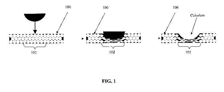
[0021] FIG. 1 illustrates the response of an example compressible photonic
crystal
material 100 suitable for use in a compressible photonic crystal-based
security and/or
authentication device when a certain area 102 of the material is compressed,
for
example by the application of mechanical pressure. In FIG. 1, a schematic
cross-
section of the photonic crystal material 100 is shown. Here, the pressure
applied to a
portion 102 of the surface of the photonic crystal collapses the ordered array
of voids
in the structure of the photonic crystal under that portion 102. In this
example, the
compression is large enough to completely collapse the structure of the
photonic
crystal 100 in the compressed portion 102, thus destroying the ability of the
compressed portion 102 to display a reflection peak. Thus, in this example,
compressed portion 102 may have substantially similar properties as a non-
porous
polymer. In the case where the uncompressed reflection peak was in the visible
spectrum, compression may result in a shift from a visible reflected color to
being
colorless (i.e., no visible reflected color).
[0022] The photonic crystal may be provided as a thin film, for example with a
thickness of less than or equal to about 100 micrometers. The voids in the
photonic
crystal may have an average diameter in the range of about 50 nm to about 1000
rim,
more preferably in the range of about 180 nm to about 900 nm. The voids may be
spherical and may be interconnected.
[0023] The photonic crystal may comprise a polymer. The polymer may be formed
from a monomer or pre-polymer selected from the group including, for example:
methacrylic acid esters, acrylic acid esters, polyisoprene, polybutadiene,
polyurethane
CA 02743985 2011-05-17
WO 2010/057307 -6- PCT/CA2009/001672
precursors, polyolefin precursors, polyethers, and mixtures thereof. The
polymer may
be a cross-linked polymer network.
[0024] In FIG. 2, a cross-section of an example design schematic of the
compressible
photonic crystal-based security and/or authentication device 200 is shown. The
device
200 includes a compressible photonic crystal 202, which in this example is
supported
on a substrate 204. The substrate 204 may be relatively flexible or relatively
rigid.
The substrate 204 may be clear, translucent, opaque, or colored, and may
incorporate
images, patterns, data content, or other such designs. Any such designs may be
viewable through a compressed portion of the photonic crystal 202 when the
device
200 is compressed. Suitable substrate materials may include, for example,
plastic
films, plastic sheets, metal foils, papers, glass, ceramics and combinations
thereof. In
some examples, the device 200 may include a protective top coating 206 or
protective
cover, A hich may include, for example, plastic films, lacquers, varnish,
latex, glass or
other suitable materials. The protective coating 206 may be relatively
flexible or
relatively rigid. The protective coating 206 may be transparent or translucent
to allow
the photonic crystal and/or the substrate to be viewable through the coating.
In some
examples, adhesives 208 may be included between the substrate 204 and the
photonic
crystal 202, and/or between the protective coating 206 and the photonic
crystal 202,
which may help to improve bonding characteristics. Where the device 200 is
designed
to be applied to an article, additional adhesives 210 may be applied to the
back of the
substrate 204 for attachment of the device 200 to an article. The additional
adhesive
210 may be applied to the photonic crystal 202 directly where the device 200
does not
include the substrate 204. The adhesives 208 and/or the additional adhesive
210 may
be selected such that it does not penetrate into the array of voids in the
photonic
crystal 202, or such that any penetration is minimal and does not affect the
ability of
the photonic crystal 202 to display a reflection peak.
[0025] In one embodiment of the security and/or authentication device, a user
would
compress the security device, and observe a disappearance of the color in the
compressed region. If the device is viewed using reflected light, the color
will be that
of the characteristic reflection peak. If the device is viewed using
transmitted light,
the color will be made up of those wavelengths complimentary to the
characteristic
reflection peak. In another embodiment, the security device could incorporate
a
CA 02743985 2011-05-17
WO 2010/057307 -7- PCT/CA2009/001672
colored background, so that a user applying a compression would perceive a
change
in color of the device in the compressed region.
[0026] In another embodiment, the background may include an image such as a
pattern, logo, picture, or data such as a barcode or alphanumeric code. Such a
background may be provided on the substrate of the device, or may be provided
on
the surface of the article to which the device is applied. The user
compressing the
device would either see the image or data appear, or cause the already visible
image
or data to change appearance. For example, FIG. 3 is a top-view illustration
of an
example of this embodiment, where pressure is applied to the security device
300 and
the compressed region 302 becomes colorless, at the same time revealing the
latent
pattern beneath.the compressed region of the device. FIG. 4 shows another
example
of this embodiment, where the device 400 is provided over a patterned
background
402. The example device 400 originally exhibits a visible reflected wavelength
that is
perceived as a green color, and after pressure is applied to a portion 404 of
the device
400, the compressed portion 404 no longer exhibits the reflected wavelength
and is
perceived as colorless and transparent, revealing the patterned background 402
underneath the device 400.
[0027] The described devices may be used, for example, as anti-counterfeit or
security devices and may be suitable for use in, for example: a) documents of
value,
including, for example, legal tender, bills of exchange, money orders, share
certificates, bonds, stamps, land titles; b) cards and identification,
including, for
example, passports, birth certificates, driver licenses, visa documents,
health cards,
social security cards, national identity cards, work permits, citizenship
documents,
alien registration documents, credit cards, debit cards, gift cards, access
passes, and
membership cards; and c) product packaging and tagging, including, for
example, that
for over-the-counter and prescription drugs, medicines and pharmaceuticals,
vaccines,
vitamins, nutritional supplements, herbal formulations, herbicides,
pesticides, apparel,
accessories, watches, clothes, shoes, handbags, cosmetics, toys, jewelry,
gems,
precious metals, compact discs, videotapes, DVDs, computer software, video
games,
other media, technology products, batteries, airline parts, auto parts, small
arms, wine,
spirits, beer, cigarettes, cigars, books, sports equipment and memorabilia,
collectibles,
CA 02743985 2011-05-17
WO 2010/057307 -8- PCT/CA2009/001672
and antiques. Other applications may be suitable, including any application
where
authentication and/or security may be useful.
Compositions
[0028] Examples of the described device may be based on a photonic crystal
including a polymer having an ordered array of spherical voids. These
spherical voids
could be isolated, or could be connected to each other to form an
interconnected array.
The polymer can be selected from a broad range of classes including, for
example,
polyacrylates, polymethacrylates, polyisoprenes, polybutadienes, polyolefins,
polyurethanes, and polyethers. The polymer may be cross-linked to form a cross-
linked network.
[0029] In an embodiment, the polymer is formed from the polymerization of
acrylic
acid esters, which could be monofunctional or multifunctional. Monofunctional
acrylic acid esters could include, for example, butoxyethyl acrylate,
hydroxyethyl
acrylate, 2-carboxyethyl acrylate, poly(2-carboxyethyl) acrylate, stearyl
acrylate,
lauryl acrylate, butyl acrylate, hexyl acrylate, 2-phenoxyethyl acrylate and
mixtures
thereof. Multifunctional acrylic acid esters could include, for example,
diacrylates,
which could include, for example, ethylene glycol diacrylate, poly(ethylene
glycol)
diacrylates, neopentyl glycol diacrylate, neopentyl glycol propoxylate (1
PO/OH)
diacrylate, triacrylates, or polyacrylates. Other polymerizable acrylate
monomers and
prepolymers may be suitable, for example those available in research sizes
from
Sigma-Aldrich, as well as from Sartomer Company.
[0030] The fabrication of the device may be carried out in a manner similar to
that
described in PCT Patent Application No. W02008098339.
[0031 ] For example, the manufacturing may include:
[0032] 1) providing an ordered array of microparticles. In some examples, the
microparticles may be necked, for example by treating the ordered array of
microparticles with tetramethoxysilane vapor or silicon tetrachloride vapor.
Necking
may affect the structural properties of the manufactured material. Necking may
also
result in interconnected voids in the manufactured material. The
microparticles may
be, for example, silica or polymer microspheres. Polymer microspheres may
include,
CA 02743985 2011-05-17
WO 2010/057307 -9- PCT/CA2009/001672
for example, polystyrene microspheres, polymethacrylate microspheres, and
mixtures
thereof.
[0033] 2) infiltrating the ordered array of microparticles with a monomer or
pre-
polymer mixture, which may include, for example, applying one of heat,
agitation,
vacuum, and pressure to the monomer or pre-polymer mixture. The monomer or pre-
polymer mixture may include an initiator, such as a photoinitiator or a
thermal
initiator.
[0034] 3) initializing cross-linking of the monomer or pre-polymer mixture to
form a
polymer. A suitable polymer may include, for example: polyacrylates,
polymethacrylates, polyisoprenes, polybutadienes, polyolefins, polyurethanes,
polyethers, and mixtures thereof.
[0035] 4) removing the microparticles from the polymer to form an ordered
array of
voids in the polymer, thereby providing a photonic crystal, which may include
etching
the microparticles using, for example, one of hydrofluoric acid, sodium
hydroxide,
and polymer solvents.
[0036] Additional steps may include providing a substrate and/or protective
coating
for the photonic crystal, examples of which are described above.
[0037] Although the above disclosure provides specific examples, these are for
the
purpose of illustration only and are not intended to be limiting. Although an
example
of manufacturing is described, the device may be manufactured by other
methods.
Although the example of manufacturing is described as having steps in a given
order,
the steps may be carried out in a different order, or some steps may be
omitted or
modified. It will be understood by a person skilled in the art that variations
and
adjustments, including simple experimentation, may be possible within the
scope of
the disclosure. All references mentioned are hereby incorporated by reference
in their
entirety.