Note : Les descriptions sont présentées dans la langue officielle dans laquelle elles ont été soumises.
CA 02751245 2016-11-28
MOLECULAR IMPRINTED NANOSENSORS
10
BACKGROUND
This disclosure is related to sensors and, more particularly, sensors
featuring
molecularly imprinted polymers.
Sensors capable of detecting specific chemical agents such as proteins have
application in a number of areas including chemical or pharmaceutical process
monitoring, environmental surveillance, early stage cancer detection, anti-
biowarfare detections, explosive detection, real time biological detections in
vivo or
in vitro, etc. In typical applications, it is desirable that the sensor be
able to identify
the presence of a specific target molecule in real time and with high
sensitivity.
Molecular imprinting is a technique to create template-shaped cavities in a
material, e.g. a polymer. The cavities act as a "memory" of the template
molecules,
and so may be used in molecular recognition. Molecularly imprinted materials
are
typically prepared using a template molecule and functional monomers that
assemble around the template and subsequently get cross linked to each other.
The
functional monomers, which are self-assembled around the template molecule by
interaction between functional groups on both the template and monomers, are
polymerized to form an imprinted matrix (commonly known as a molecularly
1
CA 02751245 2011-07-29
WO 2010/144157
PCT/US2010/023068
imprinted polymer or "MIP"). Then the template molecule is removed from the
matrix under certain conditions, leaving behind a cavity complementary in size
and
shape to the template. The obtained cavity can work as a selective binding
site for a
specific target molecule.
SUMMARY
This disclosure is directed to devices, and techniques including the
combination of a nanosensor with molecular imprinting technology. In some
embodiments, a non conductive nanocoating (e.g, a polyphenol nanocoating) is
established on a nanostructure, e.g. a conductive carbon nanotube (CNT) array.
Proteins (or other target molecules) can be incorporated with the polymer
layer and
then washed out to create protein imprinted cavities in the polymers. The
imprints
hold an intrinsic affinity to the imprinting proteins that enables specific
recognition.
The protein-polymer interaction can be measured as an impedance change,
although
other detection methods may be used. Using the imprinting method, one may be
able to detect a protein (or other target molecule) of interest without the
use of
antibodies or epitopes of antibodies.
The devices and techniques described herein may be used, for example, in
early stage cancer detection, pharmaceutical process monitoring, environmental
surveillance, anti-biowarfare detections, and real time biological detections
in vivo
or in vitro.
In one aspect, an apparatus for detecting the presence of a target molecule is
disclosed which includes a conductive nanostructure, a non-conductive polymer
coating on at least a portion of the nanostructure, and a cavity formed in the
polymer
coating having a shape corresponding to the shape of the target molecule. A
property of the nanostructure depends on the presence of the target molecule
at the
cavity.
Some embodiments include a detection unit configured to produce a signal
indicative of the presence of the target molecule at the cavity based on a
measured
change in the property of the nanostructure.
2
CA 02751245 2011-07-29
WO 2010/144157
PCT/US2010/023068
In some embodiments, the thickness of at least a portion of the non-
conductive polymer coating is less than or about equal to than the size of the
cavity.
In some embodiments the thickness of the non-conductive polymer coating is
less
than about 25 nm, less than about 15 nm, less than about 10 nm, or smaller.
In some embodiments, the polymer coating is self limiting under electro
polymerization. In some embodiments, the coating includes a polyphenol film.
In some embodiments, the nanostructure includes a carbon nanotube. In
some embodiments, the nanostructure includes an array of substantially aligned
carbon nanotubes each extending from a surface to a respective distal tip.
Some
such embodiments further include a protective layer surrounding the array such
that
only the distal tip of each nanotube extends from the layer. The non-
conductive
polymer coating includes a film on the distal tip of each nanotube.
In some embodiments, the property of the nanostructure includes the
impedance of the nanostructure. In some embodiments, the impedance of the
nanostructure depends on the presence of the target molecule at the cavity.
Some embodiments include a plurality of cavities formed in the polymer
coating each having a shape corresponding to the shape of the target molecule.
The
impedance of the nanostructure depends on the occupation of the cavities by
target
molecules.
In some embodiments, the detection unit is configured to produce a signal
indicative of the concentration of target molecules present in an environment
proximal to the nanostructure, the signal being based on the impedance of the
nanostructure. In some embodiments, the detection unit is configured to
produce a
signal indicative of the concentration of target molecules with a sensitivity
of about
10 picograms per liter or less. In some embodiments, the detection unit is
configured to produce a signal indicative of the concentration of target
molecules
with a sensitivity of about 1 picogram per liter or less. In some embodiments
the
target molecule includes ferritin.
3
CA 02751245 2011-07-29
WO 2010/144157
PCT/US2010/023068
In some embodiments, the nanostructure includes at least one from the list
consisting of: a nanoparticle, a nanorod, a nanowire, a nanotube.
In some embodiments, the property includes at least one selected from the
list of: a mechanical property, a chemical property, and electrochemical
property, an
optical property, and an electrical property.
In some embodiments, the target molecule includes at least one selected from
the list including: a protein molecule, a pheromone molecule, an explosive
molecule.
In another aspect a method is disclosed including the steps of forming a
conductive nanostructure, forming a non-conductive polymer coating on the
nanostructure in the presence of a template molecule to entrap a template
molecule
in the polymer coating, and removing the entrapped template molecule to form a
cavity in the polymer coating having a shape corresponding to the shape of the
target
molecule. A property of the nanostructure depends on the presence at the
cavity of a
target molecule having a shape corresponding to the template molecule.
In some embodiments, the thickness of at least a portion of the non-
conductive polymer coating is less than or about equal to than the size of the
cavity.
In some embodiments, the thickness of the non-conductive polymer coating
is less than about 25 nm, less than about 15 urn, less than about 10 urn, or
smaller.
In some embodiments, forming the non conductive polymer coating on the
nanostructure includes: forming a film of non-conductive polymer on a portion
of
the nanotube by electropolymerization. The final thickness of the film is self
limited
by the production of a voltage drop across the thickness of the film as it
forms on the
nanotube.
In some embodiments, forming the nanostructure includes forming a carbon
nanotube. In some embodiments, forming the nanostructure includes forming an
array of substantially aligned carbon nanotubes each extending from a surface
to a
respective distal tip. Some embodiments include forming a protective layer
surrounding the array such that only the distal tip of each nanotube extends
from the
4
CA 02751245 2011-07-29
WO 2010/144157
PCT/US2010/023068
layer. The non-conductive polymer coating includes a film the distal tip of
each
nanotube. Forming the non conductive polymer coating on the nanostructure
includes forming a non-conductive polymer film on each distal tip.
In some embodiments, removing the entrapped template molecule to form a
cavity in the polymer coating having a shape corresponding to the shape of the
target
molecule includes applying a developing fluid to the polymer coating.
In some embodiments, the developing fluid includes de-ionized water;
phosphate buffered saline; phosphate buffered saline including acetic acid or
sodium
dodecyl sulfate
Some embodiments include monitoring the property of the nanostructure to
determine information indicative of the presence of target molecule at the
cavity.
Some embodiments include determining information indicative of a
concentration of target molecules present in an environment proximal to the
nanostructure based on the impedance of the nanostructure.
In some embodiments, the determining information indicative of a
concentration of target molecules includes determining information with a
sensitivity of about 10 picograms per liter or less, or 1 picograms per liter
or less. In
some embodiments, the target molecule includes ferritin.
In some embodiments, the nanostructure includes a nanoparticle, a nanorod,
a nanowire, or a nanotube.
In some embodiments, the property includes a mechanical property, a
chemical property, an electrochemical property, an optical property, or an
electrical
property.
In another aspect, a method of selectively detecting a chemical substance is
disclosed including: providing one or more sensors. Each sensor includes: a
conductive nanostructure; a non-conductive polymer coating on at least a
portion of
the nanostructure; and a cavity formed in the polymer coating having a shape
corresponding to the shape of the target molecule (where a property of the
5
CA 02751245 2011-07-29
WO 2010/144157
PCT/US2010/023068
nanostructure depends on a presence of the target molecule at the cavity); and
a
detection unit configured to produce a signal indicative of the presence of
the target
molecule at the cavity based on a change in the property of the nanostructure.
The
method further includes using the one or more sensors, generating a signal
indicative
of the property of the nanostructure which depends on the presence of the
target
molecule at the cavity, and processing the signal to determine information
indicative
of presence of the target molecule at the cavity.
In some embodiments, for each of the one or more sensors, the thickness of
at least a portion of the non-conductive polymer coating is less than or about
equal
to than the size of the cavity.
Some embodiments include determining information indicative of a
concentration of target molecules present in an environment proximal to the
nanostructure based on the impedance of the nanostructure. Some embodiments
include determining the information indicative of the concentration of target
molecules at a sensitivity of about 10 picograms per liter or less, or 1
picogram per
liter or less.
In another aspect, a system for detecting a target molecule is disclosed which
includes a sensor array. The sensor array includes one or more sensors, each
sensor
including: a conductive nanostructure, a non-conductive polymer coating on at
least
a portion of the nanostructure, a cavity formed in the polymer coating having
a
shape corresponding to the shape of the target molecule, and a detection unit
configured to produce a signal indicative of the presence of the target
molecule at
the cavity based on a change in the property of the nanostructure. A property
of the
nanostructure depends on a presence of the target molecule at the cavity. The
system also includes a liquid coating on the sensor array and includes a gas-
liquid
interface; and a binding agent which binds with the target molecule near the
air
liquid interface, and directs the bound molecules through the liquid to the
sensor
array.
Some embodiments include a gas permeable membrane located at the gas-
liquid interface. The membrane is permeable by the target molecule.
6
In some embodiments, the binding agent releases the bound target when it
comes in proximity to the sensor array.
As used herein, the phrase "size of the cavity" is to be understood as the
length of the diameter of the smallest sphere which can encompass the entire
cavity.
A nanostructure may include an object having a characteristic size along at
least one dimensions which is on the order of tens of nanometers or less. For
example nanotubes, nanorods, or nanowires have at least two dimensions on the
nanoscale. A nanoparticle (e.g. a nanosphere) has three dimensions on the
nanoscale.
Various embodiments may include any of the features described herein,
either alone or in any combination.
Unless otherwise defined, all technical and scientific terms used herein have
the same meaning as commonly understood by one of ordinary skill in the art to
which this invention belongs. In the event that the definition of a technical
and
scientific term found elsewhere conflicts with a definition found in this
application,
the definition found in this application holds.
BRIEF DESCRIPTION OF THE DRAWINGS
Fig. 1 illustrates a molecular imprint nanosensor.
Fig. lA illustrates a molecular imprint nanosensor.
Fig. 2 illustrates the fabrication of a molecular imprint nanosensor.
Fig. 2A illustrates the fabrication of a molecular imprint nanosensor.
Fig. 2B is an SEM image of a carbon nanotube tip array (tCNTA)
Fig. 2C shows SEM images of a molecular imprient polymer on the tip of a
carbon
nanotube.
7
CA 2751245 2017-11-27
CA 02751245 2011-07-29
WO 2010/144157
PCT/US2010/023068
Fig. 3 illustrates an electrochemical device for use with a molecular imprint
nanosensor.
Fig. 4 shows three types of exemplary carbon nanotube arrays.
Fig. 5 shows electropolymerized carbon nanotubes.
Fig. 6A-6F show an atomic force microscopic characterization of a tCNTA.
Fig. 7 illustrates the trapping of a ferritin template molecule.
Fig. 8 illustrates a molecular imprint polymerization process featuring the
use of
functional monomers (fMERs)
Fig. 9 is a schematic of a circuit for electrochemical impedance spectroscopy
(EIS).
Fig. 10 illustrates a molecular imprint polymer film characterization
technique.
Fig. 11 shows an EIS measurement system for use with a molecular imprint
nanosensor.
Fig. 12 illustrates an EIS characterization technique.
Figs. 13 and 14 illustrates the detection sensitivity and selectivity of an
exemplary
molecular imprint nanosensor.
Fig. 15 is a voltagraph illustrating the impedance properties of a molecular
imprint
nanosensor.
Fig. 16 illustrates the stability of a molecular imprint polymer film under
various
conditions.
Fig. 17 is a schematic of a field effect transistor sensor.
Fig. 18A is a schematic of an integrated nanosensor device.
Fig. 18 B illustrates the operation of the device of fig, 18A.
Figs. 18C and 18D are schematics of integrated nanosensor devices.
8
CA 02751245 2011-07-29
WO 2010/144157
PCT/US2010/023068
Fig. 19 illustrates a bio-mimetic sensor system.
Figs. 20-24 illustrate exemplary results of highly sensitive and selective MIP
nanosensor based protein detection techniques.
DETAILED DESCRIPTION
MIP Sensor
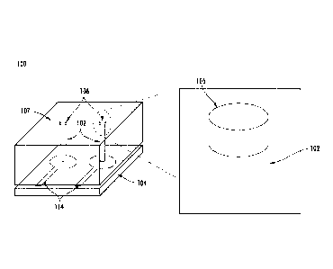
Referring to Fig. 1, in one embodiment a sensor device 100 includes one or
more nano-structures 102. As shown, the nanostructures 102 are two conductive
carbon nano-tubes (CNTs) grown vertically on a substrate 104. A portion of the
nano structure 102 is coated with a non-conductive molecularly imprinted
polymer
(MIP) 106. As shown in the inset of Fig. 1, only the tips of the CNTs are
coated
with the MIP film 106. The CNTs may be embedded in a protective material 107
(e.g. a spin coated UV cured photoresist). However, in various embodiments
other
portions or the entirety of the CNTs may be coated, e.g. as shown in Fig. 1A.
The
tips of the CNTs may be exposed or other wise extend out from a protective
material
107 (e.g. a spin coated UV cured photoresist).
As described in detail below, the MIP 106 is formed to include template
cavities 108 having shapes corresponding to a target molecule 110, as shown in
Fig.
lA (center). When the sensor device 100 is placed in the vicinity of target
molecules 110, the target molecules 110 can bind to the cavities 108 as shown
in
Fig. IA (right). Other molecules 112, having shapes which do not correspond to
that of the template cavities 108 will not bind to the cavities 108 (or will
do so much
less easily than the target molecule). The presence of the target molecules
110
bound to the MIP 106 act to change one or more physical properties of the
sensor.
In the embodiment shown, the presence of target molecules 110 in the
insulating
MIP film 104 act to reduce the resistivity of the film. In some embodiments,
the
change in the physical property may correspond to the number of cavities 108
occupied.
9
CA 02751245 2011-07-29
WO 2010/144157
PCT/US2010/023068
As described in detail below, one or more electrodes 114 couple the CNTs to
a detector unit which measures changes in one or more physical properties of
the
CNT 102 and/or the film 106, e.g. impedance changes, which indicate the
presence
of the target molecule 110.
Typically, the magnitude of change of the physical will be related to the
concentration of target molecules 110 in the environment near the CNTs. The
sensitivity of the detector 100 may be defined by the lowest such
concentration that
can be accurately and reliably detected.
In some embodiments, the thickness of the MIP film 106 is on the order of
the size of the target molecule. For example, a ferritin protein molecule has
a
diameter of about 3 iu-n. A sensor 100 of the type shown in Figs. 1 and lA may
employ an MIP film 106 having a thickness of about 10 nm. Due to the
comparable
size of the target molecule 110 and the MIP film thickness, the presence of
target
molecules 110 at the cavities 108 in the MIP film 104 may lead to relatively
large
changes in the resistivity of the film. These large changes provide a high
level of
detection sensitivity.
Fabrication
Fig. 2 illustrates the fabrication of an imprinted nanosensor 100 of the type
described above. Vertically aligned carbon nanotubes (CNTs) 102 provide the
basic
structure and surface of the sensor 100. Any suitable technique can be used to
form
the CNTs. For example, in some embodiments, a plasma enhanced chemical vapor
deposition (PECVD) process may be used for growing of an aligned CNT array.
Several types of CNT array structures may be used. For example, in some
embodiments, a high density CNT array (hCNTA) may be formed. In one such
embodiment, an area (e.g. 25x25 mm) of a silicon wafer is coated with chromium
and nickel layers of having a thickness of, e.g., 350 and 30 nm, respectively.
A base
pressure of 10-6 Ton may be used before the introduction of acetylene and
ammonia
gases. The growth pressure may be e.g. 10-2 Ton, and the growth time may be
e.g.
CA 02751245 2011-07-29
WO 2010/144157
PCT/US2010/023068
1-10 mm according to the desired nanotube length. The substrate temperature
may
be maintained below e.g. 660 C during the deposition process.
In some embodiments, a periodic and low density CNT array (ICNTA) may
be prepared. For example, in one such embodiment Ni is deposited on chromium
coated Si wafer through a polystyrene microsphere monolayer by electron beam
evaporation. Periodically patterned Ni is revealed after removal of the
spheres by
sonication. Then the Ni is annealed and plasma etched at 550 C for 2 min.
In some embodiments, a CNT tip array (tCNTA) of the type shown in Fig. 1
may be used. A tCNTA may be formed by embedding an 1CNTA in a protective
material (e.g. a photoresist) which is mechanically polished to reveal the CNT
tips
only. For example, in one such embodiment, SU8-2002 photoresist is spun on an
1CNTA (e.g. at 3000 rpm for 30 s). Following a soft bake e.g. for 5 min on a
hot
plate set at 100 C, the SUS is cross-linked by exposure to UV light for 3 mm.
Then
the sample is then hard baked, e.g. at 150 C, overnight. The resulting chip
may
then be polished e.g. until the desired tip pattern emerges from the SU8
coating as
observed with an SEM.
Fig. 4 shows scanning electron microscopy (SEM) images of hCNTA (left),
1CNTA (center) and tCNTA (right). The embedded sketches show the cross-section
of the arrays.
Referring back to Fig. 2, a non-conductive polymer 106, e.g. polyphenol, is
electropolymerized on the electrically active surface of the CNT 102 in the
presence
of a target molecule 110 (as shown, a protein). A voltage applied to the CNT
102
causes the oxidation of monomers 201 present in solution surrounding the CNTs.
This oxidation drives a polymerization process 203 to form the film 106. For
example, the inset of Fig. 2 illustrates the electropolymerization process for
a
polyphenol (PPn) film.
In embodiments where the polymer film is non-conducting, the
electropolymerization process 203 may be self limiting. Accumulated thickness
of
the non-conducting film 106 on the CNT surface results in a voltage drop
across the
11
CA 02751245 2011-07-29
WO 2010/144157
PCT/US2010/023068
film. The major reaction will stop when the voltage at the solution side of
the film is
too low to oxidize more monomers 201 (e.g. phenols).
The self-limiting deposition process allows for the reproducible and, in some
embodiments, substantially pinhole free thin film coating with nanoscale
thickness
on the order of the size of the target molecule (e.g. 10 nm or less).
The entrapped target proteins 110 can be removed by a developing buffer
leaving cavities 108 (sometimes referred to as "vials") in the film. The
topological
and conformational information of the target protein molecule 110 will be
imaged
and kept by the surface of the cavities 108, which are the imprints of the
target
protein molecule 110. The imprint holds the capability of recognition that
only
specifically allows the target protein molecule 110 with the exact match of
the
surface feature of the cavity 108 to rebind.
Due to the non-conductive nature of the nanofilm coating 106, significant
impedance (indicated in the figure as 1-2) changes will be observed at the
stage of
target protein molecule entrapment, imprint development and target rebinding.
For
molecular sensing, the signal due to the rebinding can be detected by
impedance
measurement and/or other electrochemical methods. High sensitivity will be
facilitated by the extremely thin film 106 with a thickness that is comparable
to the
size of target molecules 110. For example, proteins such as ferritin have a
characteristic size on the order of a few tens of nanometers. As noted about,
self-
limiting non-conductive polymer films with thickness of 10 nm or less may be
produced using electropolymerization.
In some embodiments, the sharp features of the coated nanostructures 102
(e.g. CNTs) may enhance the self limiting nanofilm MIP coating 106. Although
not
wishing to be limited by theory, in some embodiments this enhancement may
result
from sharp electric field gradients associated with sharp spatial features
(e.g.
extreme surface curvatures) of the CNTs. Due to the extreme curvature of CNT
surface, the electric field in the vicinity of CNTs will be intensified and
may be
helpful to produce more condensed polymer structures with higher resistivity.
Moreover, the CNT can also generate a decaying field profile, under which the
12
CA 02751245 2011-07-29
WO 2010/144157
PCT/US2010/023068
deposition could stop at a short distance from the CNT surface because of the
drop
of electrical potential.
Fig. 2A illustrates a process for fabricating an embodiment of a sensor 100
featuring a tCNTA structure. In a first step 250, an array of CNTs 102 are
formed
over electrode 114 on substrate 104. In a second step 251, the array is
embedded in
a protective material 107. For example, in one embodiment CNT array is
embedded
in SU8-2002 photoresist spun on the array at 3000 rpm for 30 seconds.
Following a
soft bake for 5 min at 100 C, the SU8 is cross-linked by exposure to UV light
for 3
min and then the sample was incubated at 150 C overnight.
In a third step 252, the embedded array is polished (e.g. using chemical
mechanical polishing, vibratory polishing, or any other suitable technique) to
expose
the tips of CNTs 102. For example, in one embodiments, the embedded array is
polished with a vibratory polisher e.g. of the type available from Buehler (41
Waukegan Road Lake Bluff, Illinois 60044 USA) with 80% power level for 6-9 hrs
until the pattern emerged from the SU8 coating with confirmation by SEM.
In a fourth step 253, an MIP film 106 is fornis on the tips of CNTs. As
described above, film 107 may be formed using an self limiting
electropolymerization process. As shown in the inset, the film 106 may be
formed
in the presence of target molecules 110, some of which are trapped in the
film. The
target molecules 110 may be removed using a developing process, leaving
corresponding cavities 108. For example, in one embodiment, the entrapped
target
molecule 100 may be a protein (as shown ferritin) entrapped in a non
conducting
polymer coating 106 (as shown PPn). For imprint development, the ferritin-
entrapping PPn coating is rinsed and incubated (e.g. overnight) in deionized
water at
room temperature. Alternatively, a developing buffer containing 5% acetic acid
and
10% sodium dodecyl sulfate (SDS) may be used for higher protein extract
efficiency.
Fig. 2B shows an SEM image of a polished CNT array after PPn coating as
in fourth step 253 (inset: the CNT cross-section showing the centered pit
after
polishing, scale bars are 2 um and 100 nm, respectively). Fig. 2C shows a TEM
13
CA 02751245 2011-07-29
WO 2010/144157
PCT/US2010/023068
images of the CNT tips where the top image is the tip of PPn, scale bar 50 nm,
and
the bottom image shows the PPn plus entrapped h_Ftn coated CNT tips (scale bar
70
nm). As shown in Figures 2B and 2C, in one embodiment, the CNT tips exhibit
open cross-sections with centered cavities. Transmission electron microscopy
(TEM) shows that the PPn was uniformly deposited on the CNT tips, forming a
pinhole-free 13 nm thick film. Co-deposition of human ferritin (hFtn) is
visualized
in the TEM image due to the contrast enhancement by the crystalline cores of
the
ferritin proteins (Fig. 2C). The diameters of the observed iron cores are
between 5
to 8 nm. The comparable values of the PPn thickness and the diameter of
protein
particle result in the huge impedance change, allowing for high detector
sensitivity.
Fig. 3 illustrates an exemplary electropolymerization system 300 for coating
an array of CNTs with a PPn film. In a three-electrode electrochemical system,
an
array of nanostructures (as shown CNT array 301) is connected as working
electrode
(W), while Ag/AgC1 and Pt wires serve as reference (R) and counter (C)
electrodes
respectively. Cyclic voltammetry (CV) is conducted by scanning voltage (e.g.
from
0 to 900 mV as shown in the left inset) between the W and C electrodes. Phenol
is
dissolved e.g. together with Na2CO3 in water. The pH may be held stable. The
reaction buffer for a typical embodiment may be 5 mM phenol supplemented
phosphate buffered saline (PBS) at pH= 7.4. The CV may be performed over
multiple cycles, e.g. five times. Of course, these electropolymerization
parameters
may be adjusted based the application at hand.
In some embodiments where a PPn film is produced, phenol is oxidized at
200 to 400 mV and produces a large peak current (illustrated in the I-V plot
of the
right inset) in the first scan 302. Due to the formation of a non-conducting
polyphenol coating on the CNT electrode, the following scans 303 typically
have a
reduced or even no oxidation current peak. In some embodiments, the current
level
may be reduced to about hundred times lower (or even less) than the first
oxidation
peak. The CNT array may maintain its original morphology with little collapse
due
to the surface tension during the sample drying after deposition. This process
may be
used to form a compact and uniform PPn coating on CNTs.
14
CA 02751245 2011-07-29
WO 2010/144157
PCT/US2010/023068
Fig. 5 (left) shows a PPn coating by transmission electron microscopy
(TEM) on both hCNTA and 1CNTA. Fig. 5 (right), is a TEM image show internal
surface coating by PPn of a top-opened CNTs that is an analogue of the tCNTA.
The
internal and external PPn exhibit the similar thickness.
As shown in Fig. 5, the self limiting electropolymerized PPn on a CNT may
form an ultra thin nanocoating e.g., with a thickness in the range of around
10-17
nm. In the example shown, the film is very uniform, compact and substantially
pinhole free. The CNT array retains its morphology after the deposition.
Further
reduction of the PPn thickness, e.g. to 7 run, may be obtained by introducing
a
dopant (e.g. sulfur) that helps to increase PPn resistivity.
Figs. 6A-6H show an atomic force microscope (AFM) characterization of a
tCNTA embedded in a protective SU8 material e.g., of the type shown in Fig. 2A
above. Figs. 6A displays the surface landscape on an as-polished carbon
nanotube
tip array (tCNTA) with no PPn coating obtained by the tapping mode scanning of
an
AFM. Fig. 6B is a plot of surface height of the same area as shown in Fig. 6A.
The
bright dots correspond to the height of the polished CNTs. In the example
shown,
the various progress rates of CNT growth and the filling SUS in which there
CNTs
are embedded resulted in the different heights.. Fig. 6C shows the cross
section
along the X'd line in Fig. 6B. As show, the height of CNT tips protruding out
of the
SU8 surface is about 9 nm. Figure 6C shows the distribution of pixel heights
in Fig.
6B. The two peaks are corresponding to the average heights of SU8 surface
structures and the CNT tips. The typical height of CNT tips is indicated by
the
distance between the two peaks, which equals to 9 nm.
Figs. 6E displays the surface landscape on an as-polished carbon nanotube
tip array (tCNTA) with a ferritin entrapping PPn coating obtained by the
tapping
mode scanning of an AFM. Fig. 6F is a plot of surface height of the same area
as
shown in Fig. 6E. The bright dots correspond to the height of the PPn coated
tips of
CNTs. Fig. 6G shows the cross section along the X'd line in Fig. 6F. As show,
the
height of coated CNT tips protruding out of the SU8 surface is about 9 nm.
Figure
6G shows the distribution of pixel heights in Fig. 6F. The two peaks are
corresponding to the average heights of SU8 surface structures and the CNT
tips.
CA 02751245 2011-07-29
WO 2010/144157
PCT/US2010/023068
The typical height of CNT tips is indicated by the distance between the two
peaks,
which equals to 28 nm.
Taking the results of the above AFM measurements together, in this
embodiment, the average thickness of PPn coating is about 9 nm, in agreement
with
observation with TEM.
As will be understood by those skilled in the art, in various embodiments, a
variety of factors may determine the thickness of the MIP film 106. According
to the
mechanism of self-limiting coating processes, the thickness is determined by
how
fast the polymerization reaction can be stopped by the insulation of
electrode. So the
MIP resistivity, porosity, oxidation voltage, polymerization level, and the
distribution of electric field etc can contribute to the thickness
determination.
Various embodiments described herein use cyclic voltammetry for the
deposition.
In such cases, the reaction rate in the polymerization may affect the density
of the
MIP film, therefore change the resistivity of the coating. In some
embodiments, the
nature of the electrode material used in the electropolymerization process may
have
significant influence on the anodic oxidation. Metals such as copper, nickel,
chromium, platinum, gold, zinc and titanium typically exhibit different values
of
potentials of oxidation. For example, oxidation of phenolic monomer occurs
more
readily on the surfaces of noble metals such as platinum and gold. Similarly,
carbon
or functionalized carbon surfaces may prime the oxidation differently, so that
the
PPn film formation may happen in different fashion than metal surfaces. In
some
embodiments, one may utilize surface chemistry to modify CNT, e.g. with amine,
carboxyl, or carbonyl groups, or to generate more defects in the carbon
surface. The
reactive sites and their densities on CNT may contribute differently to the
polymerization.
Referring to Fig. 8, in some embodiments, one may facilitate imprint
stability and specificity in the MIP film 106 by using designed cross-linking
monomers (cMer) and functional monomers (fMer) in the electropolymerization
process.. Generically, molecular imprint of synthetic polymers is a process
where
functional and cross-linking monomers are co-polymerized in the presence of
the
template proteins or other molecules (i.e. the target molecules 110).
16
CA 02751245 2011-07-29
WO 2010/144157
PCT/US2010/023068
The functional monomers initially form a complex 801 with the protein
target molecule 110 and, following polymerization, their functional groups are
held
in position by the highly cross-linked polymeric structure of the MIP film
106. The
template molecule can then be dissolved to reveal the imprint binding site
cavities
108 that are complementary in size and shape to the templates.
In the previously presented examples (e.g. as shown in Figs. 2 and 2A), the
target protein 110 was simply entrapped in the PPn coating 106 without the
assist of
fMers. In such cases the only specific information of the template protein
being
imaged on the imprint cavity 108 was the protein morphology. In order to
improve
the specificity, one can introduce a functional monomer to the deposition
system or
design a cross-linking monomer that has certain side-groups. One strategy is
shown
in Figure 8. The fMer molecule 800 is made "sticky" to form H-bonds or to
exert
electrostatic attraction etc. in one end, while another end is made reactive
to form
covalent linkage during the electropolymerization. For example, several ionic
liquid
molecules listed in Fig, 8 have a negative charged carboxyl group and a
phenolic
group on each side respectively. Upon mixing with the target proteins 110, the
pre-
complex 801 will be formed after the fMers are adsorbed by the charged
residues on
the protein surface. In some embodiments, the phenol side will be left outside
and
can be linked to other polyphenols later when electropolymerization starts.
Following the removal of proteins from the PPn coating, imprint cavities 108
with
the fMer SOO decorations on their surfaces will exhibit more selectivity to
the target
proteins 110 because of the request of matching of the charge signature in the
cavities 108. In other embodiments, a cross-linking monomer (cMer) branched by
charged/polarized side groups may be used.. For a given application, any
suitable
cMer know in the art may be used including:3-nitrophenol, pyrogallol, 4-
hydroxybenzenesulfonic acid, bromophenol blue, n-Aminophenol, 3-methyphenol,
3-nitrophenol, 1,n-dihydroxybenzene, 1,x,ytrihydroxybenzene, 5-amino-1-
naphthalene, acetaminophen, poly(1,3-diaminobenzene) , poly( p-
chlorophenylamide), etc.
17
CA 02751245 2011-07-29
WO 2010/144157
PCT/US2010/023068
Referring back to Fig. 3, in some embodiments, the film 106 has a thickness
which is relatively insensitive to voltammetry scanning rate of
electropolymerization
system 300. For example, as shown in the Table 1 below, for the PPn formation
process described above, changing the voltammetry scanning rate between 20 and
100 mV/s may not significantly alter the film thickness.
Table 1
Dopant Dopant Free Na2S
Scan rate (mV/s) 10 50 100 50
Thickness (nni) 15 17 16 7.5
As illustrated in Fig. 2, the development of the MIP includes two major
steps: (1) target molecule entrapment (e.g. in PPn); and (2) target molecule
elusion
from the entrapping layer.
A ferritin protein target molecule has a pI ¨4.5, which means the protein
carries positive charge at neutral buffer. When mixed with phenol deposition
buffer,
ferritin will be attracted to anode and co-deposition on the anode, i.e. the
CNT
sensor, surface with polyphenol.
For example, the TEM image of Fig. 7 (top left) shows ferritin molecules
immobilized on bare CNT surface by amide linkages formed between the free
amines on ferritin and carboxyl groups on the functionalized CNT. The diameter
of
the iron crystal core in the ferritin molecule is around 5 run. The TEM image
of Fig.
7 (top right) shows ferritin entrapped in the PPn coating on CNT. The whole
area of
this image is subjected to energy dispersive spectroscopy (EDS) Fig, 7
(bottom)
shows the results of the spectroscopy. The presence of ferritin is confirmed
by the
peaks of iron, which are not observed in the non-ferritin samples.
18
CA 02751245 2011-07-29
WO 2010/144157
PCT/US2010/023068
MIP target molecule elusion may be accomplished by washing the trapped
molecules from the polymer layer. For example, in some embodiments, for
protein
removal, i.e. imprint development, a sensor with ferritin entrapped PPn
coating may
be rinsed and incubated overnight in deionized water (diW) at room
temperature.
Alternatively, a developing buffer containing 5% acetic acid and 10% sodium
dodecyl sulfate (SDS) may be used instead of diW for higher protein extract
efficiency. In such cases elusion may take place in about 1 hr, about 15
minutes, or
even less. In other embodiments, PBS may be used as a developer, alone or in
combination with diW.
The development speed has been found to vary depending on the properties
of the imprinted target molecule. Accordingly, in various embodiments, the
imprint
development protocol should be adjusted to match the properties of each kind
of
proteins that include size, surface charge, subdomain and subunits etc. Figure
9
shows the theoretically calculated surface charge of several biomarker
proteins as a
function of pH. "E6 typel6" carries positive charges at pH 7.5 to 9. But other
three
biomarkers "E7 typel6", "E7 typel8", and "pRb" are negatively charged at the
same
range. Therefore, more basic (pH>9) buffer solutions will be needed in order
to have
"E6 typel6" showing the same result of a surface charge sensitive procedure as
with
other proteins. In some embodiments, it is important to record the buffer p1-1
at
which electropolymerization is conducted. The recorded pH needs to be used for
biomarker rebinding buffer during a detection process. This may be especially
important when fMers are used, since the charge profiles indicated by fMers in
the
imprints could be no longer matched to the protein surface at different pH.
In some embodiments, the removal of the template protein from the MIP
nanocoating could be facilitated by purposeful adjustment of the pH. For
example, if
the electropolymerization is done at basic solution, then reducing pH could be
helpful to facilitate the protein elusion by eliminating the electrostatic
attraction
between charged side residues of the proteins and the imprint cavities. In
some
embodiments, the effect of pH should take effect faster than any other elusion
buffers because the nanocoating as a polymer network is more permeable to
protons
19
CA 02751245 2011-07-29
WO 2010/144157
PCT/US2010/023068
t
than other molecules. In this way, the time of harsh chemical treatments will
be
shortened, and consequently have the integrity of imprint structures better
preserved.
In view of the above, it may be important to evaluate the imprint
development and/or rebinding efficiency of a given device or process in order
to
optimize the performance of sensor 100. There are several ways to evaluate the
imprint development and/or rebinding efficiency. As described in detail below,
EIS
can be used to monitor the progress of imprinting and rebinding etc. TEM can
be
used to assess protein entrapment as well. However, for many applications,
protein
molecules have too low contrast in compare with the polymer coating to be
visualized. An exception is ferritin, which has an iron-crystalline core to
differentiate itself from the adjacent materials under TEM.
In some embodiments, e.g. where TEM evaluation is impractical, the quality
and amount of imprints can be measured using an imprint refilling method. For
example, referring to Fig. 10, an MIP sensor 100 undergoes a second, post
development electropolymerization with PPn so that PPn can fill in the imprint
cavities 110. The volume of PPn that fills (Vrefill) the imprint can be
calculated
according to the charge generated at the refilling step. It can be converted
to the
amount of target molecule imprints 108. In one particular case of our
preliminary
studies, each CNT 102 may carry about 300 or more imprints. In fact, not all
of the
volume taken by the refilling PPn can be refilled by proteins. As illustrated
in Fig.
10, Vrefill may also give an indication of the damage 1001 caused to MIP film
106
during the development processing. This information can be used to optimize
the
development process to reduce or minimize unwanted damage.
Detection
As noted above, using sensors 100 of the type described herein, the presence
of a target molecule 110 may be detected by sensing a change in a physical
property
of the sensor's nanostructures 102 due to interaction of the MIP film coating
106
with target molecules 110.
CA 02751245 2011-07-29
WO 2010/144157
PCT/US2010/023068
For example, in some embodiments, the sensor may include a three terminal
electrochemical cell of the type shown in Fig. 3. Electrochemical impedance
spectroscopy (EIS) may be used to measure changes in the impedance of the
electrochemical cell in response to the application of target molecules.
In one such embodiment, monitoring of the electrochemical behavior of the
MIP thin-film may be conducted with a Reference 600 electrochemical system
produced by Gamry Inc. (Warminster, PA), running under the control of Gamry
Framework software. Data analysis is conducted with Gamry's Echem Analyst
software. Fig. 11 shows an exemplary detection circuit for EIS. This EIS set
up
may be used to determine the impedance Zcdi of the cell, and, in turn, to
monitor for
the presence of the target molecule.
Figs. 12 illustrates an exemplary EIS analysis of an embodiment of a CNT
array MIP sensor designed to detect the presence of ferritin. Electrochemical
impedance spectroscopy (EIS) is conducted before and after PPn deposition to
evaluate the impedance property of CNT array electrode surface and its
interface to
a surrounding buffer solution. The circuit is driven with a sine wave with a
10 mV of
peak-to-peak amplitude. The sine wave is superimposed with a 300 mV DC
voltage.
The frequency of the sine wave is scanned from 1 Hz to 1 MHz.
During the measurement, ferrocene carboxylic acid is supplemented to the
PBS buffer in which the sensor 100 is immersed at final concentration 1 mM.
The
impedance data are fitted to an electrical equivalent circuit using the
impedance
analysis function in the Gamry Echem Analyst software. The equivalent circuit
provides an electrical analogue of thin film coating and chemical/physical
processes.
Mono-frequency (e.g. without frequency scanning) EIS is also used to monitor
the
protein binding dynamics. In this case, sine wave and DC voltage remained the
same
as that of frequency scanning.
Fig. 13A shows Nyquist plots of real and imaginary impedance resulting
from EIS of the nanosensor 100. As described above, frequency is scanned from
1
Hz to 1 MHz. Three bold traces represent sensors of bare CNT (no PPn), with
ferritin entrapped in the PPn film (PPn+Frtn) and imprints formation after the
21
CA 02751245 2011-07-29
WO 2010/144157
PCT/US2010/023068
ferritin removal (Imprinted PPn). The other traces represent measurements
taken
with the sensor immersed in a buffer solution having ferritin present at
different
concentrations (10-12, 10-11, 10-1 , 10-9, 10, and 10-7 g/L). Note that the
Nyquist
plot for ferritin concentrations of 10-12 g/L can be clearly distinguished
from the plot
corresponding to no ferritin. This indicates that the presence of ferritin can
be
detected at concentrations on the order of picogams per liter.
Fig. 13B shows protein dose responses in impedance and faradic current of
the sensor in the presence of ferritin and, alternatively, in the presence of
bovine
serum albumin (BSA). Measurements are plotted for the ferritin concentrations
listed immediately above. Measurements are plotted for the bovine serum
albumin
(BSA) at concentrations of 10-16, 10-9, 10-8, 10-7, 10-6, 10-5, 10-4 and 10-3
g/L. In the
top panel, sensor impedances measured at 10 Hz are plotted. The dashed line
indicates the initial impedance before BSA applications. Faradic currents
obtained
from differential pulse voltammetry (DPV) are shown in the bottom panel. Each
method (mono-frequency EIS and DPV) shows similar dosage responses to BSA
and ferritin respectively. However, as measured by either technique, BSA needs
more than 106 times higher concentration than ferritin to produce a similar
change in
the impedance. This demonstrates a high selectivity of the imprints to
ferritin
molecules.
This selectivity ensures that the sensor will be highly sensitive to the
presence of the target model, and relatively very insensitive to other
molecule types.
Accordingly, the sensor is well suited for the detection of the target
molecule, even
in the presence of one or more types of "noise" molecules.
MIP Film Characterization
The EIS techniques described above may also be used to characterize MIP
films deposited on the nanostructures. For example, Fig. 14 shows the results
of EIS
evaluation of the PPn coating on the different CNT array types (hCNTA, 1CNTA,
and tCNTA). Fig. 14A shows a comparison of Nyquist plots before (no PPn) and
after PPn (PPn) coatings on the three CNT arrays. The frequency is scanned
from 1
Hz to 1 MHz. Fig. 14B shows the complex impedance change of the tCNTA due to
22
CA 02751245 2011-07-29
WO 2010/144157
PCT/US2010/023068
the PPn coating. The parameters a and j3 represent the multiple by which the
real
and imaginary parts of the impedance have been elevated by the presence of the
PPn. Four separate recordings are superimposed. Two of the scans are started
from
0.1 Hz, while the other two range from 1 Hz. Figure 14C shows the impedance
modes measured at 10 Hz before and after PPn coating for the CNT array types.
The
numbers above the columns denote the impedance ratio that is obtained by the
impedance with PPn divided by the impedance without PPn.
The above evaluation demonstrates that PPn on CNT sensor can dramatically
increase the impedance, especially at low frequency such as 3 Hz, where the
Zreal
and Ziff,,,g are elevated nearly 20 (a) and 80 (13) times respectively for a
tCNTA array
as shown in Figure 9B. Such an impedance difference offers a large dynamic
range
for detecting imprinting induced impedance change.
PPn MIP film stability may be evaluated using cyclic voltammetry
techniques of the type described above. For example, Fig. 15 shows a cyclic
voltagram taken for a CNT sample (with and without PPn) immersed in a PBS
buffer supplemented with ferrocyne carboxylic acid (FCA). As shown, the peak
current is reduced by more than two orders of magnitude by the PPn film. Thus,
the
anodic peak current of the voltagram clearly serves an indication of the
presence and
integrity of the PPn coating.
Accordingly, measurement of the CV anodic peak may be used to explore f
the stability of the PPn film under various conditions. For example, the
tables below
shows that PPn coating can dramatically reduce the FCA current from ¨15 A to
nA
or even pA range. Degradation of the PPn film under various conditions may be
may be explored by measurement of increases of the measured peak current. For
example, Table II shows exemplary peak current values for PPN coated CNT array
samples immersed for various time intervals (0, 10, 20, and 30 min) in various
organic solvents. For example, after exposure to methanol for 10 minutes, the
peak
current of Sample B increased in magnitude from 433 nA to -1.400 A,
indicating
some degredation of the PPn film.
Table II
23
CA 02751245 2011-07-29
WO 2010/144157
PCT/US2010/023068
Peak Current
Sample A
FCA before PPn -16.83 A -12.66/LA -13.02 A
FCA after PPn -1.658 /IA -433 nA -376.2 nA
Solvent Methanol Ethanol Acetone
FCA after 10 min -8.457 /LA -1.400 A -1.164 ILA
FCA after 20 min -800 nA -1.331 itA
FCA after 30 min -1.405 A
Similarly, the Table III shows exemplary peak current values for a PPN
coated CNT array sample baked on a hot plate for 10 minutes at various
temperatures (40, 60, 80, and 100 C). note that heating results in only a
modest
increasing in peak current, indicating that the PPn film is relatively stable
under
these thermal conditions.
Table III
Sample C Peak Current
FCA after PPn -706.2 nA -730.1 nA -641.0 nA
FCA after 10 min at 40 C -717.2 nA -742.3 nA -737.7 nA
FCA after 10 min at 60 C -741.5 nA -744.7 nA -798.5 nA
FCA after 10 min at 80 C -661.1 nA -699.8 nA -791.5 nA
FCA after 10 mm at 100 C -638.6 nA -683.2 nA -773.7 nA
Table IV shows exemplary peak current values for PPN coated CNT array samples
incubated in buffers supplemented by surfactants of various types (SDS, Tween-
20,
NP-40, and Triton x-100) for various times.
Table IV
24
CA 02751245 2011-07-29
WO 2010/144157
PCT/US2010/023068
Peak Current
Sample A B D C
FCA before surfactant -148.1 nA -6.260 nA -4.125 nA -6.445 nA
Surfactant SDS (1%) Tween-20 ( NP-40 (1%) Triton x-100
FCA after 1 hr -4.532 nA -1.827 nA -199.2 pA -2.315 nA
FCA after 8 hrs -76.37 nA -115.5 nA -136.6 nA -1.047 nA
FCA after 12 hrs -300.0 pA -18.21 pA -1.860 nA -173.0 pA
FCA after 24 hrs -7.537 nA -1.475 nA -898.5 pA -13.88 nA
Table V shows exemplary peak current values for PPN coated CNT array
samples incubated in buffers at a given pH range for various times. As shown,
the
pH range was measured at the various time intervals to detect and possible pH
drift.
Table V
Peak Current
Sample A B D C
FCA before pk -121.0 pA -837.2 pA -8.192 nA
-667.5 pA
pH at 0 hrs 1.0-1.2 4.1-4.4 4.9-5.1 12
FCA at 0 hrs -3.346 pA. -81.96 pA -675.1 nA
-344.6 nA
pH at 1 hr 1.0-1.2 4.4 5.5.-5.8 11
FCA at 1 hr -6.757 1..LA -762.2 nA -673.7 nA
-696.5 nA
pH at 4 hrs 1.0-1.2 4.4 5.5-5.8 11
FCA at 4 hrs -1.149 A -794.5 nA -689.2 nA
-836.0 nA
pH at 12 hrs 1.0-1.2 4.4-4.8 5.8 9-10
FCA at 12 hrs -1.707 /LA -855.0 nA -688.5 nA
-867.5 nA
CA 02751245 2011-07-29
WO 2010/144157
PCT/US2010/023068
Similarly, Fig. 16 summarizes the effects of organic solvents, temperature,
surfactants and pH on PPn stability were presented based on the peak current
of CV.
The above measurements demonstrate that PPn films exhibit good thermal
stability at the testing conditions. The PPn remains stable in contact with
different
kinds of surfactants including ionic (SDS) and non-ionic (Tween 20, Triton x-
100
and NP-40) ones. Some organic solvents (methanol) and pH (acidic) may lead to
some changes in the FCA currents,
Alternate Sensor Embodiments
The examples of sensor 100 above feature MIP layers 106 on vertically
aligned CNT arrays. However, it is to be understood that sensor 100 may
include
other types of MIP coated nanostructures. The nano structures may include
nanowires, nanorods, nanoparticles, nancones, etc. Nanostructures 102 may be
made of any suitable material including metals (Au, Ag, Ti, Mo, metal alloys,
etc.),
semiconductors such as Si (doped or undoped), conductive polymers, a
conductive
oxide (e.g. ZnO) etc. The nanostructures may be arranged in any geometry
including regular arrays, irregular arrays, random arrays. The nanostructures
may be
vertically arranged (i.e. extending perpendicular to a substrate),
horizontally
arranged (i.e. extending parallel to a substrate), or arranged at any
intermediate
angle.
In one embodiment, the sensor 100 includes a mesh of conductive nanotubes
or nanowires (a "nanomesh") coated with an MIP film 106. In some embodiments,
the mesh may lay substantially flat on an underlying substrate 104. As with
CNT's
the electrical properties (e.g. impedance) of the mesh changes in the presence
of a
target molecule 110 having a shape corresponding to that of imprinted cavities
108
in the MIP film 106.
In another embodiment, the sensor 100 includes one or more graphene sheets
with an MIP film 106, e.g. formed on a silicon substrate 104. As with CNT's
the
electrical properties (e.g. impedance) of the coated graphene sheets changes
in the
26
CA 02751245 2011-07-29
WO 2010/144157
PCT/US2010/023068
presence of a target molecule 110 having a shape corresponding to that of
imprinted
cavities 108 in the MIP film 106.
In another embodiment, the sensor 100 includes an array of Si nanowires
coated with MIP film 106. As with CNT's the electrical properties (e.g.
impedance)
of the coated nanowire array changes in the presence of a target molecule 110
having a shape corresponding to that of imprinted cavities 108 in the MIP film
106.
Field Effect Transistor Based Nanosensor
Referring to Fig. 17, in some embodiments the sensor 100 is arranged as a
field effect transistor (PET). As shown, a nanostructure 102 (e.g. a nanotube,
nanowire, nanomesh, graphene sheet, nanowire array, etc) is located on glass
substrate 104. The nanostructure 102 is coated with an MIP layer 106, and is
disposed between source and drain electrodes 1701, 1702. A sample buffer 1703
is
located over the MIP layer 106, and is in electrical contact with gate
electrode 1704.
As in previous example, the electrical properties (e.g. impedance) of the
coated
nanostructure 102 changes in the presence of a target molecule 110 having a
shape
corresponding to that of imprinted cavities 108 in the MIP film 106.
Accordingly,
the behavior of the FET will differ in the presence of the target molecule
110. In
one embodiment, the voltage difference between the gate electrode 1704 and the
drain electrode may be varied while the source-drain current is measured. The
presence of the target molecule 110 will register as a change in the
relationship
between the gate voltage and the source/drain current.
Integrated Nanosensors
In some embodiments one or more sensors 100 may be integrated in a single
device. When a plurality of the sensors 100 are used, different sensors 100
may be
imprinted to detect different target molecules 110.
For example, referring to Figs. 18A and 18B, integrated sensor device 1800,
includes MIP sensors labeled 1, 2, 3, and 4. Sensor 1 is a control which has
not been
imprinted with a target molecule. Each sensor of sensors 2, 3, and 4 has been
imprinted with a different target molecule (proteins E7 type 16, E7 type 18,
and E6
27
CA 02751245 2011-07-29
WO 2010/144157
PCT/US2010/023068
type 16, respectively). Each sensor may be independently addressed by a
corresponding set of electrodes to provide a signal indicative of the presence
of the
corresponding target molecule. For example, one or more sensors may be
independently addressable by an EIS detection system as described above. In
some
embodiments, one or more sensors may be an independently addressable FET
sensor
of the type described above.
Samples to be tested may be introduced to the sensors via a microfluidic
channel 1801 having an inlet 1802 and an outlet 1803. The channel may include
one
or more microfluidic elements to control the flow of sample to the sensors.
The use
of micro fluidics allows for highly sensitive control over the sample flow
rate.
Fig. 18B illustrates the electrical response of the sensors to serial and
parallel
application of sample fluids including the various the target molecules. As
shown,
the sensors can output unique signals indicative of the presence or absence of
each
target molecule, either alone or in combination.
In one embodiments, the sensors are fabricated on a silicon substrate. Each
sensor may be very compact, e.g. about 1 square millimeter or less. In some
embodiments, the sensors may be fabricated as follows. The different target
molecules may be separately prepared in a single kind of electropolymerization
buffer. By switching buffer inputs and electrical active terminals, each
target
molecule may be selectively deposited to the designated sensor unit. Then the
entire
device 1800 may then be rinsed with the protein removal buffer (or imprint
developer) to reveal the imprints and make the sensor functionally available.
Fig. 18D shows an alternate embodiment of the integrated sensor device
1800 featuring four sensors Si, S2, S3, and S4, each of which includes five
sensors
imprinted with a respective target molecule. The sensors are formed on a SiC
coated
Si wafer. Electrodes (e.g. ti electrodes) for each sensor (e.g. electrodes
labeled Ul 1 -
U15 corresponding to the five sensors is the set S1) are patterned on the SiC
surface.
28
CA 02751245 2011-07-29
WO 2010/144157
PCT/US2010/023068
Integrated sensors of the type described above may be fabricated using any
suitable technique know in the art, including photolithographic techniques,
micro-
electromechanical system (MEMS) fabrication techniques, etc.
Biomimetic Sensor
The inventors have realized that sensor system designs may be based on
naturally occurring sensory organs, e.g. insect olfactory organ (e.g. the
sensory hair
on a silkworm antennae). For example, referring to Fig. 19, a bio-mimetic
sensor
system 1900 includes a one or more (e.g. an array of) MIP coated nanostructure
sensors 100 of the type described above. As above, the M1P sensor is imprinted
with a target molecule 110 in order to provide sensitive and highly selective
detection of the target molecule 110. The MIP sensor 100 thus operates in a
manner
similar to the olfactory receptors in an insect olfactory organ.
The MIP sensor 100 is immersed in a thin layer of liquid 1901(or other fluid
or gel) with a gas liquid interface 1902. This liquid layer mimics the
sensillar lymph
surrounding the neuronal dendrites in an insect sense organ.
The liquid interface 1902 may be covered with a gas permeable membrane
which allows the target molecule 110 to permeate through the membrane into the
liquid. This membrane mimics the cuticle of the insect organ. The membrane may
be hydrophobic, and thus relatively impenetrable by liquids. Examples of gas
permeable membranes include macroporous polytetrafluorethylene (PTFE) and
silicone rubber.
Binding agents 1903 are present in the liquid which mimic pheromone-
binding-protein found in insect olfactory organs. The binding agent molecules
1903
selectively bind to target molecules 110 which have diffused into the liquid.
Once
bound, the target molecules 110 are carried in the direction of the MIP sensor
100.
Once in proximity to the MIP sensor 100, the binding molecules 1903 release
the
target molecules. For example, the binding molecules 1903 may dissociate with
the
binding molecule in response to a controlled pH in the vicinity of the MIP
sensor
100.
29
CA 02751245 2011-07-29
WO 2010/144157
PCT/US2010/023068
Sensors of this type have a number of applications, including chemical
detection, such as explosive detection. Target molecules 110, which may have a
very low concentration, diffuse across the membrane and are directed by the
binding
agents to concentrate in proximity to the MIP sensors 100. Processor 1904 can
monitor the signals from sensor 100 to determine the presence and/ or
concentration
a target molecule. When the concentration near the sensor 100 becomes greater
than
the minimum sensitivity of the sensor 100, indicating the presence of the
target
molecule 110, the processor 1904 may trigger an alarm or provide another
suitable
output.. For example, in one embodiment, the sensor system may be used to
inspect
cargo or luggage for the presence of trace amounts of an explosive, such as
trinitrotoluene.
Processing and Analysis
Any of the sensors described herein may feature a monitor or analysis
processing unit which receives signals from the MIP sensor indicative of the
presence of the target molecule. The signals may be analyzed, e.g., by a
digital
computer. The computer may output information based on these signasl, and/or
control one or more other devices based on the analysis. For example, in an
embodiment where the sensor system is employed to detect the presence of
explosives, a signal indicative of the presence of an explosive chemical could
trigger
an alarm. In embodiments where the sensor system is employed to monitor a
chemical process, a signal indicative of the presence of, or a certain
concentration
of, a target molecule could trigger an automatic modification on one or more
of the
processes parameters (e.g. temperature, pH, etc.). As will be understood by
one
skilled in the art, the sensor devices and techniques described herein can
similarly be
adapted to numerous applications.
Some embodiments may feature multiple MIP sensors, possibly fabricated to
be sensitive to different target molecules. In such embodiments, a processor
may
analyze information indicative of the simultaneous presence and/or the
relative
concentration of multiple target molecules, and determine output or control
actions
based on this information.
CA 02751245 2011-07-29
WO 2010/144157
PCT/US2010/023068
Any of the analysis methods described herein can be implemented in
hardware or software, or a combination of both. The methods can be implemented
in
computer programs using standard programming techniques following the method
and figures described herein. Program code is applied to input data to perform
the
functions described herein and generate output information. The output
information
is applied to one or more output devices such as a display monitor, or may be
used
to automatically control one or more devices or systems. Each program may be
implemented in a high level procedural or object oriented programming language
to
communicate with a computer system. However, the programs can be implemented
in assembly or machine language, if desired. In any case, the language can be
a
compiled or interpreted language. Moreover, the program can run on dedicated
integrated circuits preprogrammed for that purpose.
Each such computer program is preferably stored on a storage medium or
device (e.g., ROM or magnetic diskette) readable by a general or special
purpose
programmable computer, for configuring and operating the computer when the
storage media or device is read by the computer to perform the procedures
described
herein. The computer program can also reside in cache or main memory during
program execution. The analysis method can also be implemented as a computer-
readable storage medium, configured with a computer program, where the storage
medium so configured causes a computer to operate in a specific and predefined
manner to perform the functions described herein.
Example: Ultrasensitive Detection of Proteins
From disease diagnosis to laboratory proteomic study, monoclonal
antibodies ( mAbs) are one of the key elements for biorecognition; however,
they
are problematic due to their high cost, low stability, and compromised
specificity.
Polymeric molecular imprints (MI) could be used as artificial antigen
receptors
thereby replacing mAbs . However the progress towards an ultrasensitive
imprinted
sensor, particularly for proteins, has been fairly slow, although the
technical concept
was recorded thirty years ago. Here, we report our significant advance in an
imprinted protein sensor, believed to be 104 times more sensitive than
previous
devices having e.g. minimum detectable human ferritin concentrations of 20 aM
by
31
CA 02751245 2011-07-29
WO 2010/144157
PCT/US2010/023068
electrochemical impedance spectroscopy. Further, using the devices and
techniques
described herein, robust selectivity may be demonstrated with other proteins,
binary
samples, and cellular protein extracts. Moreover, Ca2+ induced calmodulin
conformational change was sensitively detected. The molecular imprinted
nanosensor affords sensitive antibody-free protein detection, and holds
promise for
applications in those instances where antibodies, aptamers, or natural ligands
are not
available, or where protein conformational changes reduce sensor
functionality.
MI polymers may be used as bulky materials for chromatographic
separations, antibody-free ligand-binding assays, and selective sample
enrichment
by solid-phase extraction. MI polymers may be applied as films on electrodes
lacking nanostructures to detect small organic molecules. Protein imprinting
strategies may be used as well. However, the detection limits of such
techniques
are typically on the jig/ml level, which are not comparable to the sensitivity
of
embodiments of the nanosensors described herein.
Not wishing to be bound by theory, this may be due, in part, to several
factors: 1) the fragility and complexity of the protein molecules, which make
them
vulnerable to the imprinting chemistry; 2) MIP films on non-nano structures
are too
thick to exert remarkable signals corresponding to the targets, particularly
when
their concentrations are low; 3) the detection mechanisms do not allow for
effective
signal conversion of the target bindings; and 4) the basal sensor
architectures are not
supportive of highly sensitive detection.
In various embodiments, the nanosensor herein overcomes many of these
obstacles, by imprinting a non-conducting polymer nanocoating on the tips of
carbon nanotube (CNT) arrays, e.g. as described above. The protein of
interest, or
template protein, is initially incorporated within the nanocoating. Upon
imprint
development, i.e. removal of the proteins from the superficial part of the
nanocoating, the sensor electrical impedance is greatly reduced due to
electrical
leakage through the surface voids left behind by the imprints in the
nanocoating.
Subsequent re-binding of the target protein into these voids is detected as an
increase
of impedance, due to the relatively lower conductivity of the target protein.
The
fabrication and detection procedures are illustrated in Figure 2A, discussed
in detail
32
CA 02751245 2011-07-29
WO 2010/144157
PCT/US2010/023068
above. Notably, the nonconductive polymeric nanocoating was generated on CNT
tips by electropolymerization of polyphenol (PPn). This self-limiting
deposition
process affords both convenience and highly conformal nanocoating with uniform
thickness. Such nonconductive nanocoating was preferred to low noise
recordings,
and beneficial for highly sensitive detection. EIS measurements indicated that
the
PPn coating on the tips of the CNT arrays exhibited the highest impedance
improvement among a variety of arrays. An additional reason to construct the
sensor architecture with CNT tips was that electrochemical detection can be
facilitated with faster electron transfer kinetics on nanotube tips than on
nanotube
side walls.
The embedded proteins on the outer surface of the PPn coating could be
readily removed by sodium dodecyl sulphate (SDS)-supplemented phosphate
buffered saline (PBS). The change in sensor impedance corresponding to the
protein
removal was measured by EIS. A subsequent refilling experiment of the type
described above was conducted by electropolymerizing PPn into the voids of the
post-imprinted sensor, to evaluate the number of potential imprint sites on
the
sensor. According to the total charge generated at the initial PPn coating
(140
degrees C) and at the refilled state (30 degrees C), we estimate that the
volume
occupation of the imprints was about 21% of the total polymerized PPn. This
charge
could then be used to calculate the number of imprinted hFtn molecules. In one
particular case, we calculated that each CNT carried ¨300 hFtn imprints.
The hFtn detection was conducted with EIS as well as differential pulse
voltammetry (DPV). As shown in Figure 20A, Nyquist plots demonstrate the
impedance spectroscopy of the sensor at different stages of development and
various
levels of protein rebinding. The hypothetical impedance changes mentioned
above
were well demonstrated. Compared to bare sensor arrays (no PPn), the PPn
coating
(PPni-hFtn) increased the sensor impedance modulus from 13 2 IS) to 241 47
k.C2
(data obtained from 7 samples, f=10 Hz). The impedance vs. protein
concentrations
demonstrates apparent different responses for different targets. Each hFtn
measurement was preceded by the measurement of a control protein, bovine serum
33
CA 02751245 2011-07-29
WO 2010/144157
PCT/US2010/023068
albumin (BSA), to emphasize the contrast of the responses to ferritin and BSA.
Application of hFtn in concentrations ranging from 10-12 to 10-7 g/L exhibited
an
increase in impedance, whereas BSA exhibited significantly smaller changes in
impedance, even at 10-3 g/L. The impedance modulus at 10 Hz showed that the
response to hFtn started between 10-12 and 10-" g/L, while that of BSA was
between
10-4 and 10-2 g/L. Therefore, a 106 higher concentration of BSA was required
to
generate a similar impedance signal. The impedance approached its maximum
value
with 10-7 g/L of hFtn. Thus, the dynamic range of hFtn detection spans 4
decades.
To verify the detection of ferritin, DPV was used to detect the faradic
current
corresponding to the insulation leakage by the imprints. Fig. 20B shows dose
responses of faradic current vs. protein concentrations, on log ¨ log scales.
The
inset is the original DPV current responding to different hFtn concentrations.
The
blockage of DPV current by hFtn rebinding exhibited similar dose response as
that
observed with EIS. Control experiments were conducted using other proteins
such
as horse apoferritin (aFtn) and horse ferritin (hsFtn) with concentrations up
to 10-4
g/L. These control molecules did not exhibit significant effects via either
EIS or
DPV. Note that ferritin is a very conservative protein in mammalians, with
hFtn and
hsFtn having more than 92% homogeneity. Thus, discrimination of the two
ferritins
suggests a high selectivity of the sensor. The binary protein mixtures
containing
hFtn and other interfering protein molecules such as aFtn, hsFtn and a whole
protein
extracts from another animal were also evaluated.
As shown in Figure 20C, all binary mixtures exhibited DPV inhibition above
the non-specific current reduction by the interfering proteins; the hFtn
concentration
was 1/100 of the interfering proteins. The sensor selectivity to hFtn in
binary
mixtures shown by DPV. All interferent proteins were prepared at 1 p.g/L with
each
binary protein mixture prepared by mixing hFtn with the interferent protein at
the
final concentrations of 0.01 and 1 !AWL, respectively).
To elucidate the mechanisms of the detection, Nyquist plots were fitted with
a model containing constant phase elements (CPE), as shown in Fig. 21A. Rp is
generally considered the PPn coating resistance. R,, is the solution
resistance. When
ao in CPE0 is close to 1, Ao represents the double layer capacitance Cal. For
PPn-
34
CA 02751245 2011-07-29
WO 2010/144157
PCT/US2010/023068
coated electrodes, Ao is considered the capacitance of serial Cdl and CpPn.
Accordingly, the observed impedance changes in "PPn coated" and "MI" sensors
can be attributed to the alterations of resistance and capacitance. Fig. 21B
shows Rp
and Ao at various fabrication stages, such as "CNT only", "PPn coated" and
"MI"
(molecularly imprinted) derived from Nyquist plots fittings. Their values are
displayed in log scales.)
Accordingly, the previous dose-response in EIS can be described as the
increase of resistance and decrease of capacitance vs. the increase of hFtn
concentrations (see Fig. 21C, showing Rp and AD vs. administrated ferritin and
BSA
concentrations). At the highest hFtn concentration, we observed a 50%
resistance
increase and a 20% capacitance decrease. In contrast, the non-specific binding
of
BSA showed an obscure fashion of resistance and capacitance changes.
The ferritin detection data shown in Figure 21C can be presented, as shown
in Figure 21E, as the percentage change of impedance modulus (AZmod) as a
function
of ferritin concentration. As shown in the inset, the data is fitted to a
cooperative
model, resulting in a dissociation constant of the imprint to ferritin at 53.6
pg/L. In
other words, the data indicates that the above described technique is
sufficiently
sensitive that ferritin can be reliably detected at concentrations of 53.6
pg/L or less.
Fig. 21D illustrates possible scenarios of the sensors surfaces. Four
scenarios of sensor surface conditions closely related to resistivity (p) and
permittivity (c): ((1) bare nanotube surface, where solution double-layer
dominates
the surface, (4120, Pbuffer), (2) nanotube surface coated by PPn, (eppn,
pppn); (3)
nanotube coated by PPn with imprint vials, (61120/PPn, Pbuffer(PPn); and (4)
imprint with
re-bound template protein, (
,EproteiniPPn, Pprotein/PPn))= The change of permittivity (c) and
resistivity (p) in the surface materials are considered as the primary
mechanism of
the signaling. In brief, re-hinging proteins have lower sand higher p than the
displaced water in the imprint space, leading to increased resistance and
decreased
capacitance.
CA 02751245 2011-07-29
WO 2010/144157
PCT/US2010/023068
We also sought to determine if molecular imprinting could discriminate
protein conformations. The protein calmodulin (CaM) was employed, due to its
Ca+2 dependent conformations. The conformational change was biochemically
demonstrated by gel-shift experiments. Figure 22A shows SDS denatured gel test
of
Ca 2+ induced CaM conformation change. Ca2+ (1 mM) was balanced with EGTA at
various concentrations. The gradual band shift indicates the native Ca2+
dependency
of CaM conformation.
During the co-deposition phase with PPn, 1 mM Ca2+ was used to saturate
CaM and render a full scale elongation ("open") that offered distinctive
imprint
morphology from its globular shape at Ca2+ free or other partial "close"
status. Ca2+
bound CaM (Ca-CaM) was detected by DPV under various free Ca2+ concentration
buffered with ethylene glycol tetraacetic acid (EGTA). As shown in Figure 22C,
this result was confirmed using circular dichroism measurement, in which the
degree
of conformation change in CaM as a function of Ca2+ concentration is a buffer
solution are detected using a circular dichroism (CD) technique. As is well
known
in the art, CD is the differential absorption of left- and right-handed
circularly
polarized light.be a substance. A CD spectrometermay be used to record this
phenomenon as a function of wavelength and chemical environment. Fig. 22C
shows the CaM CD fractional angular displacement measured as a function of
wavelength for various concentrations of Ca2+ in an EGTA buffer. The measured
angular displacement correspondsto the Ca2+ binng induced CaM conformation
change. Given the molecular weight of CaM is 16.8 Kd, the CaM concentration in
the measurement was 5.34 p.M that, at certain points, allowed all Ca-binding
sites
being saturated by the Ca2+ in the buffer. The fractional angular
displacements at
208 nm are fitted in the inset with the equation including cooperative
information.
Figure 22B shows sensor DPV peak currents inhibited by Ca-CaM. (Peak
currents were normalized to that recorded in Tris buffer with 1 mM EGTA. In
all
other recordings, 10 mg/L CaM was added to the Tris-EGTA buffer. Addition of
different amounts of CaC12 yielded the designated free [Ca2]. Imprint-
independent
current represents the total residual current that was not sensitive to even
overloaded
ca2+. KdEoyA _
207 nM. n=4. Error bars stand for S.E.M.). DPV current was
36
CA 02751245 2011-07-29
WO 2010/144157
PCT/US2010/023068
inhibited at 0.2 nM free Ca2+ and exhibited a half maximum inhibition at
approximately 1 nM, reflecting a high sensitivity and selectivity to Ca-CaM.
In summary, the sensor reported herein offers the advantage of highly
sensitive, label-free detection of proteins, with a detection limit of ¨10
pg/L hFtn,
equivalent to 20 aM, a 104 times improvement over previous imprint-based
"peptide" sensors, and 100 times greater sensitivity than antibody-based
nanosensors. The present molecular imprint-based detection scheme also offers
flexibility for the detection of a range of molecules, from organic compounds
to
macromolecules. Moreover, it may prove useful for detecting conformational
changes in proteins that might be incurred as a result of post-translational
modification, mutation or ligand binding. Finally, the sensor holds promise
for the
detection of macromolecules in situations where conventional means of
detection
(e.g. antibody-based recognition) are not feasible.
In the above example, periodic CNT arrays were first prepared as described
above. The arrays were then modified by spin coating a SU8 photopolyrner film
followed by mechanically polishing to expose the tips of the CNTs. A PPn film
was
deposited on the exposed tips by cyclic voltammetry in PBS containing 1.5 mM
phenol (pH = 7.4). The array was then connected as a working electrode.
Potential
was scanned 5 times from 0 to 0.9 V versus a reference electrode at 50 mV/s.
In
order to entrap ferritin in the PPn nanocoating, the protein was added to the
PPn
deposition buffer at 100 ug/ml. Following electrophoretic attraction by
applying
300 mV DC voltage for 30 s, cyclic voltammetric voltages were used to form PPn
as
previously mentioned, with the co-deposition of ferritin. For EIS
measurements, a
10 mV peak-to-peak sine wave was superimposed on a 300 mV DC voltage. DPV
was conducted with initial and final potentials settings of 0 and 0.5 V,
respectively.
Other parameters defined by the manufacturer were set as: pulse size 50 mV,
pulse
time 0.05 s; step size 2 mV, and sample period 0.1 s. Imprint development was
based on previous described procedures.
37
CA 02751245 2011-07-29
WO 2010/144157
PCT/US2010/023068
Example: Detection of HPV Biomarker
Cervical cancer is worldwide the second most common cancer in women. It
is estimated that annually there are over 470,000 new cases and 233,000
deaths.
Detecting cancers in the pre-malignant state is critically important, as early
detection
would allow for appropriate treatment modalities to be initiated prior to the
onset of
metastasis, thereby reducing mortality and morbidity, potentially
significantly so.
Research has revealed that nearly all cervical cancers (99.7%) are directly
linked to previous infection with one or more of the oncogenic types of HPV.
There
are total about 100 kinds of HPV with some of them malignancy related and
termed
as ''high risk" virus. Therefore, unlike other cancers, the early detection of
cervical
cancer has two concerns: (1) identifying if there is high-risk virus; and (2)
examining if there are oncogenisis signals that indicate malignancy of the
tissue.
Biomarkers are biological substances (such as, nucleic acid, lipids, or
proteins) that
can be used to detect disease (particularly for cancers), measure its
progression, or
monitor the efficacy of therapeutic intervention. The diagnostic biomarkers
detection techniques in use today are not only insufficient of early
detection, but
may also suffer from a lack of sensitivity or specificity.
In the HPV genome, a significant role for malignant transformation can be
assigned to the early gene E6 and E7 genes and their respective proteins. Both
E6
and E7 proteins can bind to multiple cellular targets. Initial observations
revealed
that E6 interacts with p53 , and E7 interacts with pRb to block the activity
of these
tumour suppressors. Indeed, some of the prominent functions of the E6 protein
originate from its interaction with, followed by degradation of p53, and the
pro-
apoptotic protein Bak, which results in resistance to apoptosis and an
increase in
chromosomal instability. E7, however, interacts with pRb-associated pocket
proteins, which are negative cell cycle regulators involved in the Gl/S and
G2/M
transitions. The interaction between E7 and pRb results in enhanced
phosphorylation
and degradation of pRb. pRb destruction leads to the release of the
transcription
factor E2F, upregulates p16 (i.e. 1NK4A) and subsequent activation of genes
promoting cell proliferation. Since E6, E7, p53, pRb, and p16 proteins are
closely
38
CA 02751245 2011-07-29
WO 2010/144157
PCT/US2010/023068
related to HPV induced pathogenesis, they are considered as biomarkers of
cervical
cancer.
MIP nanosensors of the type described herein can be provide highly sensitive
and selective detection of biomarkers, e.g. those associated with pathogenic
HPV.
For example, referring to Fig. 23, MIP nanosensor was imprinted with the E7
type
16 protein. The peak current response of the sensor is plotted against sample
concentration for a variety of E6 and E7 proteins. As shown, the sensor
exhibits
significant response to E6 type 16 at concentrations as low as about 0.1 pg/L.
Further, the sensor is highly selective for E6 type 16, as demonstrated by the
clearly
distinguishable response to E7 type 18 and E6 type 16 proteins.
It is to be understood that although the specific example of detecting HPV
biomarkers have been discussed in detail, the above describe techniques can be
applied for use in detecting other biomarkers, e.g. those associated with the
H1N1
influenza virus.
Example: Streptavidin Imprint
Referring to Fig. 24, we used streptavidin to imprint the PPn coated tips of a
tCNTA sensor using the techniques described herein. After the rebinding of
streptavidin was electrochemically observed as with protein detection as
described
above. Tthe sample was incubated at room temperature with PBS buffer
supplemented with biotinylated gold particles for 20 min. Following rinse, the
sample was fixed with 3.7% formaldehyde. As shown in Fig. 24, tips (one shown,
indicated with a dashed circle)of the tCNTA were imaged with an SEM. The
biotinylated gold particles associated with (i.e. bonded to) the streptavidin
molecules
bound to the imprinted PPn coating are visible as bright dots on the SEM
image.
Thus, the number of gold particles mentioned above is an indirect indication
of the
streptavidin. On average, there were 40 gold particles per nanotubes. A
control
sample was coated with unimprinted PPn only but experienced the same process
as
the imprint sample. No particle was observed on the CNT tips of the control.
39
CA 02751245 2011-07-29
WO 2010/144157
PCT/US2010/023068
Additional Embodiments
A number of embodiments are described herein. Nevertheless, it will be
understood that various modifications may be made without departing from the
spirit
and scope of the invention.
For example, although several of the embodiments described herein feature
conductive CNTs, other nanostructures can be used including conductive, non-
conductive, or semi-conductive nanostructures. The nanostructures may include
nanowires, nanorods, nanoparticles, or a combination thereof The
nanostructures
may be arranged in any suitable configuration, including vertically,
horizontally,
randomly, etc.
Although several embodiments described herein feature PPn MIP films,
other suitable films may be used. For example, phenolic oxide polymers can be
used for the same sensor development by electropolymerizing phenol, p-cresol,
4-
chlorophenol, 2,4-dichlorophenol, pyrogallol, 3-nitrophenol, 4-hydroxybenzene-
sulfonoc acid, bromophenol blue, etc. Other suitable non-conductive polymers
include poly(indole), poly(o-phenylene-diamine), poly(7,14-
diphenylacenaphtho[1,2-k]fluoranthene), etc. Some embodiments may include
imprinting conductive or semi-conductive polymer nanocoating on
nanostructures.
The typical conductive polymers include poly(pyrrole), poly(n-methyl pyrrole)
and
poly(aniline).
Although several embodiments described herein feature impedance
measurements to determine the presence of a target molecule, any measurement
scheme may be used. For example, any physical, chemical, electrochemical,
optical,
electrical or any other suitable property of the nanostructure and/or MW film
may be
used.
Examples of suitable electrochemical detection methods include:
chronoamperornetry, chronocoulometry, chronopotentiometry, cyclic voltammetry,
linear sweep voltammetry, differential pulse voltammetry, square wave
voltammetry, normal pulse voltammetry, reverse normal pulse voltammetry,
CA 02751245 2011-07-29
WO 2010/144157
PCT/US2010/023068
differential pulse stripping voltammetry, square wave stripping voltammetry,
normal
pulse stripping voltammetry, reverse normal pulse stripping voltammetry,
galvanostatic EIS (electrochemistry impedance spectroscopy), hybrid EIS,
potentiostatic EIS, single frequency EIS.
In some embodiments, the target molecules may include a fluorescent tag,
and detection may include detection of light from target molecules trapped by
the
MIP.
In some embodiments, the imprint techniques described herein may by
applied to target structures other than molecules.
Other aspects, features, and advantages are within the scope of the invention.
41